

Page 1

DATA SH EET
Objective specification
Supersedes data of 1998 Apr 15
File under Integrated Circuits, IC02
1999 Sep 16
INTEGRATED CIRCUITS
TDA8798
Dual 8-bit, 100 Msps A/D converter
with DPGA
Page 2
1999 Sep 16 2
Philips Semiconductors Objective specification
Dual 8-bit, 100 Msps A/D converter with
DPGA
TDA8798
FEATURES
• Dual 8-bit Analog-to-Digital Converter (ADC)
• Sampling rate up to 100 million samples per
second (Msps)
• Dual 34 dBV 6-bit Digitally Programmable Gain
Amplifier (DPGA) with optional power-off
• Optional external equalization filter with capacitive
coupling between DPGA and ADC
• Serial Interface (SI) for DPGA gain control using either
parallel load mode or count-up/count-down mode
• 3.3 V TTL/CMOS compatible I/O
• Differential or single-ended TTL/CMOS clock interface
• AC or DC coupling for DPGA inputs.
APPLICATIONS
• High-dynamic range acquisition front-ends
• Digital data storage read channels.
GENERAL DESCRIPTION
The TDA8798 is a dual 8-bit ADC with DPGA.
The 100 Mspsmaximumsamplingrateand34 dBVDPGA
gain range optimizes the ADC for high dynamic range
applications.
QUICK REFERENCE DATA
SYMBOL PARAMETER CONDITIONS MIN. TYP. MAX. UNIT
V
DDA
analog supply voltage 3.15 3.3 3.45 V
V
DDD
digital supply voltage 3.0 3.3 3.6 V
V
DDO
output stage supply voltage 2.7 3.3 3.6 V
I
DDA
analog supply current with DPGAEN LOW − 106 − mA
with DPGAEN HIGH − tbf − mA
I
DDD
digital supply current − 30 − mA
I
DDO
output stage supply current − 3 − mA
INL DC integral non-linearity from IC analog input to digital
output; ramp input;
f
CLK
= 100 MHz
with DPGA at G
(min)
−±3.0 tbf LSB
without DPGA −±1.0 tbf LSB
DNL DC differential non-linearity from IC analog input to digital
output; ramp input;
f
CLK
= 100 MHz
with DPGA at G
(min)
−±0.5 tbf LSB
without DPGA −±0.5 tbf LSB
V
n(o)(rms)
output referred noise (RMS value) DPGA at G
(max)
; Zi =50Ω;
noise bandwidth = 15 MHz
− tbf 2 mV
rms
B
(−3dB)(ADC)
ADC −3 dB analogue bandwidth at V
i(dif)(FS)
− 120 − MHz
B
(−3dB)(DPGA)
DPGA −3 dB bandwidth at V
i(dif)(max)
30 tbf − MHz
f
(sample)(max)
maximum sampling rate 100 −−Msps
P
tot
total power dissipation with DPGAEN LOW − 460 500 mW
with DPGAEN HIGH − tbf tbf mW
Page 3
1999 Sep 16 3
Philips Semiconductors Objective specification
Dual 8-bit, 100 Msps A/D converter with
DPGA
TDA8798
ORDERING INFORMATION
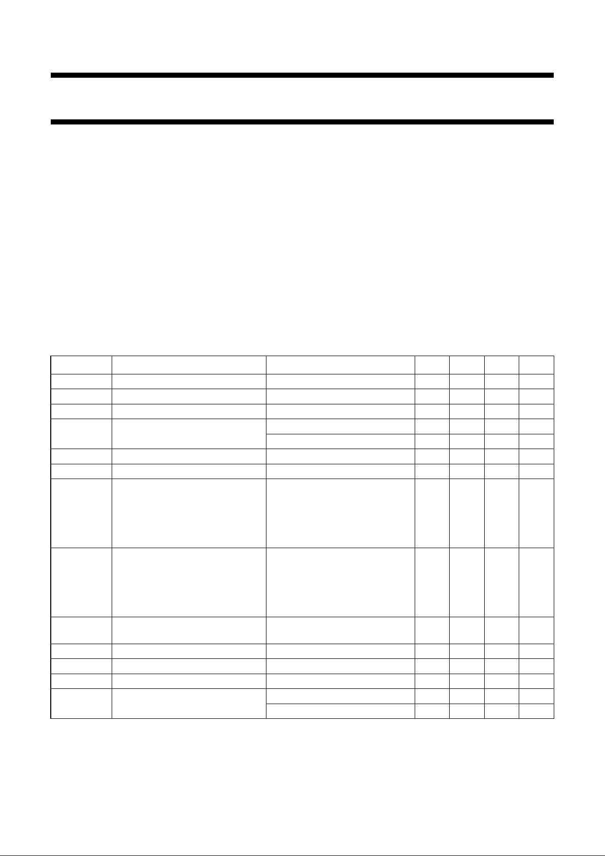
BLOCK DIAGRAM
TYPE
NUMBER
PACKAGE
NAME DESCRIPTION VERSION
TDA8798HL LQFP64 plastic low profile quad flat package; 64 leads;
body 10 × 10 × 1.4 mm
SOT314-2
Fig.1 Block diagram.
handbook, full pagewidth
MGM863
OPTIONAL
EXTERNAL
FILTER 2
SERIAL
INTERFACE
DPGA2
DPGA1
BUFFER
SR
58
59
52
V
DDA4
61 51
V
SSA4
6055
TEST
REGULATOR
54
V
oref2
V
oref1
62
BUF2
64
BUF2N
63
DPGA2N
1
DPGA2
to DPGA2
to DPGA2N
to BUF2
to BUF2N
OPTIONAL
EXTERNAL
FILTER 1
to DPGA1N
to DPGA1
to BUF1N
to BUF1
2
DPGAC2
V
DDO2
V
SSA3
BUF1DPGA1NDPGAC1
V
SSO1
V
DDO1
V
DDA3
BUF1NDPGA1
3
6
VIN2N
7
VIN2
10
VIN1
11
VIN1N
5
V
DDA2
8
V
SSA2
24
V
SSD1
25
V
DDD1
56
V
DDD2
53
DPGAEN
57
V
SSD2
9
V
SSA1
12
6
V
DDA1
325031212019
1718161514
41 to 48
4
29
26
28
30
13
40 to 33
23
22
CLK2N
CLK2
digital
output 2
B0 to B7
V
ref2
27
SEN2
SCLK
SMODE
SDATA
SEN1
V
ref1
digital
output 1
A0 to A7
analog
input 2
analog
input 1
CLK1
CLK1N
V
SSO2
49
BUFFER
TE
OE
A
D
A
D
TDA8798
REGULATOR
ADC1
ADC2
6
Page 4
1999 Sep 16 4
Philips Semiconductors Objective specification
Dual 8-bit, 100 Msps A/D converter with
DPGA
TDA8798
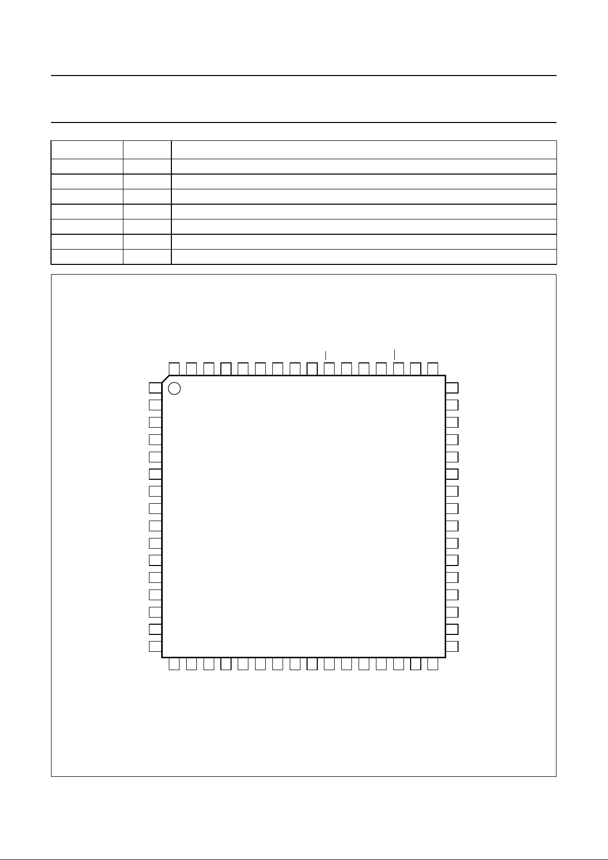
PINNING
SYMBOL PIN DESCRIPTION
DPGA2N 1 DPGA2 inverting output
DPGA2 2 DPGA2 non-inverting output
DPGAC2 3 DPGA2 bandwidth limitation control
V
ref2
4 ADC2 reference output
V
DDA2
5 DPGA2 analog supply voltage
VIN2N 6 DPGA2 inverting input voltage
VIN2 7 DPGA2 non-inverting input voltage
V
SSA2
8 DPGA2 analog ground
V
SSA1
9 DPGA1 analog ground
VIN1 10 DPGA1 non-inverting input voltage
VIN1N 11 DPGA1 inverting input voltage
V
DDA1
12 DPGA1 analog supply voltage
V
ref1
13 ADC1 reference output
DPGAC1 14 DPGA1 bandwidth limitation control
DPGA1 15 DPGA1 non-inverting output
DPGA1N 16 DPGA1 inverting output
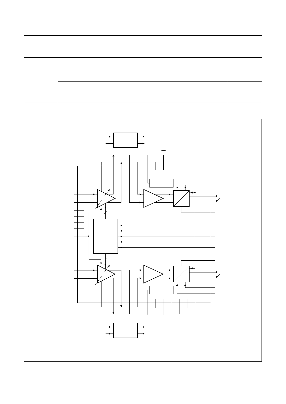
Fig.2 External filter.
External filtering may be used between DPGA and ADC to limit the noise bandwidth.
The external filterhasalow-passcut-offfrequency of .
and a high-pass cut-off frequency of
.
Other types of filter may be used if DC biasing is correct.
f
l 3dB–()
1
2π
------ -
R2⁄ R
oDPGA()
+
L
------------------------------------------
×≈
f
h 3dB–()
1
2π
------ -
1
R
iADC()
C×
----------------------------- -
×≈
(1) DPGA1/DPGA2
(2) BUF1/BUF2
(3) DPGA1N/DPGA2N
(4) BUF1N/BUF2N
handbook, full pagewidth
FCE267
I
OUT
−
I
OUT
C
o(DPGA)
TDA8798 TDA8798
10 µH
L
10 µH
100 nF
100 nF
C
C
L
C
o(DPGA)
R
o(DPGA)
DPGA
(1)
BUF
(2)
BUFN
(4)
R
1 kΩ
DPGAN
(3)
R
o(DPGA)
R
i(ADC)
R
i(ADC)
C
i(ADC)
C
i(ADC)
Page 5
1999 Sep 16 5
Philips Semiconductors Objective specification
Dual 8-bit, 100 Msps A/D converter with
DPGA
TDA8798
BUF1 17 buffer1 non-inverting input
BUF1N 18 buffer1 inverting input
V
oref1
19 buffer1 common mode reference output
V
DDA3
20 ADC1 analog supply voltage 3
V
SSA3
21 ADC1 analog ground 3
CLK1N 22 ADC1 inverting clock input
CLK1 23 ADC1 non-inverting clock input
V
SSD1
24 digital ground 1
V
DDD1
25 digital supply voltage 1
SMODE 26 serial interface mode input
SEN2 27 serial interface enable 2 (active low)
SDATA 28 serial interface data input
SCLK 29 serial interface clock input
SEN1 30 serial interface enable 1 (active low)
V
DDO1
31 output stage supply voltage 1
V
SSO1
32 output stage ground 1
A7 33 channel 1 output bit 7 (MSB)
A6 34 channel 1 output bit 6
A5 35 channel 1 output bit 5
A4 36 channel 1 output bit 4
A3 37 channel 1 output bit 3
A2 38 channel 1 output bit 2
A1 39 channel 1 output bit 1
A0 40 channel 1 output bit 0 (LSB)
B0 41 channel 2 output bit 0 (LSB)
B1 42 channel 2 output bit 1
B2 43 channel 2 output bit 2
B3 44 channel 2 output bit 3
B4 45 channel 2 output bit 4
B5 46 channel 2 output bit 5
B6 47 channel 2 output bit 6
B7 48 channel 2 output bit 7 (MSB)
V
SSO2
49 output stage ground 2
V
DDO2
50 output stage supply voltage 2
OE 51 digital output enable (active LOW)
SR 52 digital output bit slew-rate control
DPGAEN 53 DPGA enable (active LOW)
TEST 54 test input (to be grounded)
TE 55 track-and-hold enable (active LOW)
V
DDD2
56 digital supply voltage 2
V
SSD2
57 digital ground 2
SYMBOL PIN DESCRIPTION
Page 6
1999 Sep 16 6
Philips Semiconductors Objective specification
Dual 8-bit, 100 Msps A/D converter with
DPGA
TDA8798
CLK2 58 ADC2 non-inverting clock input
CLK2N 59 ADC2 inverting clock input
V
SSA4
60 ADC2 analog ground 4
V
DDA4
61 ADC2 analog supply voltage 4
V
oref2
62 buffer2 common mode reference output
BUF2N 63 buffer2 inverting input
BUF2 64 buffer2 non-inverting input
SYMBOL PIN DESCRIPTION
Fig.3 Pin configuration.
handbook, full pagewidth
TDA8798HL
MGM864
1
2
3
4
5
6
7
8
9
10
11
12
13
14
15
16
48
47
46
45
44
43
42
41
40
39
38
37
36
35
34
33
B7
B6
B5
B4
B3
B2
B1
B0
A0
A1
A2
A3
A4
A5
A6
A7
DPGA2N
DPGA2
DPGAC2
V
ref2
V
DDA2
VIN2N
VIN2
V
SSA2
V
SSA1
VIN1
VIN1N
V
DDA1
V
ref1
DPGAC1
DPGA1
DPGA1N
17
18
19
20
21
22
23
24
25
26
27
28
29
30
31
32
64
63
62
61
60
59
58
57
56
55
54
53
52
51
50
49
BUF2
BUF2N
V
oref2
V
DDA4
V
SSA4
CLK2N
CLK2
V
SSD2
V
DDD2
TEST
DPGAEN
SR
V
DDO2
V
SSO2
BUF1
BUF1N
V
oref1
V
DDA3
V
SSA3
CLK1N
CLK1
V
SSD1
V
DDD1
SMODE
SEN2
SDATA
SCLK
SEN1
V
DDO1
V
SSO1
TE
OE
Page 7

1999 Sep 16 7
Philips Semiconductors Objective specification
Dual 8-bit, 100 Msps A/D converter with
DPGA
TDA8798
FUNCTIONAL DESCRIPTION
The TDA8798 comprises two independent fully differential
signalchainseachhavingaDPGAandahigh-speed ADC.
A serial interface allows the gain of each DPGA to be
controlledindependently. To improve signal conditions, an
AC-coupled external filter can be connected between a
DPGAandADC.TheTDA8798canbeused as a dual 8-bit
ADC without DPGA functionality, using less power.
Digitally Programmable Gain Amplifier (DPGA)
The gain of the differential DPGA is programmable from
0 to 34 dBV in 63 equal steps by a 6-bit word output in
parallel from a gain control register in the SI. For all gain
settings, the DPGA signal bandwidth exceeds 30 MHz.
The settling time between gain changes can be adjusted
by an external decoupling capacitor connected to
DPGAC1 (pin 14) and/or DPGAC2 (pin 3). The analog
input signals can be either AC or DC coupled. When used
only as a dual 8-bit ADC, both DPGAs can be disabled to
reduce power consumption.
Analog-to-Digital Converter (ADC)
The 8-bit ADC converts the differential analog input signal
into a binary output format at a maximum conversion rate
of 100 Msps. All digital input and output signals are
TTL/CMOS compatible.
The ADC clock signal can be from either a differential or a
single-ended source; when single-ended, the unused
clockinputpinshouldbe decoupled externally. The analog
input to the ADC is AC coupled.
Whenused only as a dualADC, the ADC can beexternally
biased by regulator output V
oref1
(pin 19) and/or
V
oref2
(pin 62) using series resistors of, for example, 50 Ω,
connected to the ADCbuffer inputs providing a lower input
impedance. This requires V
oref1
and/or V
oref2
to be
decoupled to ground by a 10 nF capacitor.
V
ref1
(pin 13) and/or V
ref2
(pin 4) provide a voltage
corresponding to the bias of the ADC which can be used
as a reference output to an external control circuit.
Alternatively, an external control voltage can be applied to
these pins to adjust the full-scale range of the ADC.
Serial Interface (SI)
The SI allows the gain of each DPGA to be controlled
independently using either a parallel load mode or a
count-up/count-down mode. The gain control mode is
selected by the state of SMODE. The operation of DPGA
gain control is shown in Timing diagram, (see Fig.4).
Parallel load mode
This mode loads gain control data serially into a decoder
in the SI. Each of the six bits are loaded on the rising edge
ofSCLK.After the load has completed, SEN goes inactive,
loading the data in parallel to a gain control register in the
SI, changing the gain of the DPGA.
Count-up/count-down mode
Count-up/count-down mode is selected when SMODE is
in the opposite state to parallel load mode. This mode
either increments or decrements the SI gain control
register in one-bit steps when SEN and SCLK are both
active; the state of SDATA determines the count direction
(up or down). This allows the gain of the DPGA to be
changed asynchronously and intermittently.
ADC digital outputs
Digital noise on the internal supply lines increases when
the V
DDO
voltage increases, affecting the crosstalk
between channels. This effect can be reduced by making
SR (pin 52) HIGH, changing the slew-rate of the ADC
digital outputs.
Page 8
1999 Sep 16 8
Philips Semiconductors Objective specification
Dual 8-bit, 100 Msps A/D converter with
DPGA
TDA8798
Table 1 Serial interface truth table; see notes 1 and 2
Notes
1. ‘← Di’: shifting LSB and loading new LSB with value Di.
2. In count-up/count-down mode, thegain control register cannotbe incremented above themaximum gain value of 63,
or decremented below the minimum gain value of 0.
SMODE SCLK SEN1 SEN2 SDATA ACTION
0 1 1 U WAIT
0 1 1 Di SISR: SISR ← Di
0 0 1 1 SISR: SISR ← 1
GCR1: GCR1 + 1
0 0 1 0 SISR: SISR ← 0
GCR1: GCR1 − 1
0 1 0 1 SISR: SISR ← 1
GCR2: GCR2 + 1
0 1 0 0 SISR: SISR ← 0
GCR2: GCR2 − 1
0 0 0 1 SISR: SISR ← 1
GCR1: GCR1 + 1
GCR2: GCR2 + 1
0 0 0 0 SISR: SISR ← 0
GCR1: GCR1 − 1
GCR2: GCR2 − 1
1 U WAIT
1 Di SISR: SISR ← Di
1 U GCR1: SISR
1 U GCR2: SISR
1 U GCR1: SISR
GCR2: SISR
X,
X, X, X,
X, X,
X, X,
X, X,
X,
Page 9

1999 Sep 16 9
Philips Semiconductors Objective specification
Dual 8-bit, 100 Msps A/D converter with
DPGA
TDA8798
Table 2 Abbreviations
Table 3
TE truth table
Table 4 SR truth table
Table 5 DPGAEN truth table
Table 6 Gain Control
SYMBOL DESCRIPTION
GCR1 DPGA1 gain control register value
GCR2 DPGA2 gain control register value
SISR Serial interface shift register value
X can be either logic state 0 or logic
state 1
rising edge
falling edge
U can be either undefined logic stateX
rising edge or falling edge
Di Data input
TE ADC TRACK-AND-HOLD
0 track-and-hold enabled
1 track enabled
SR ADC DIGITAL OUTPUT SLEW RATE
0 maximum
1 minimum
DPGAEN DPGA FUNCTIONALITY
0 enabled
1 disabled
GAIN CONTROL
REGISTER VALUE
GAIN (dBV)
000000 0.00
000001 0.54
000010 1.08
... ...
... ...
... ...
111110 33.46
111111 34.00
LIMITING VALUES
In accordance with the Absolute Maximum Rating System (IEC 134).
SYMBOL PARAMETER CONDITIONS MIN. MAX. UNIT
V
DDA
analog supply voltage −0.3 +7.0 V
V
DDD
digital supply voltage −0.3 +7.0 V
V
DDO
output stage supply voltage −0.3 +7.0 V
∆V
DDX
supply voltage differences between
V
DDA
and V
DDD
−1.0 +1.0 V
V
DDO
and V
DDD
−1.0 +1.0 V
V
DDA
and V
DDO
−1.0 +1.0 V
V
i(VIN)
input voltage range on VIN1 and VIN2
(pins 10 and 7)
referenced to V
SSA
−0.3 +7.0 V
I
O
output current − 10 mA
T
stg
storage temperature −55 +150 °C
T
amb
ambient temperature 0 70 °C
T
j
junction temperature − 104 °C
Page 10

1999 Sep 16 10
Philips Semiconductors Objective specification
Dual 8-bit, 100 Msps A/D converter with
DPGA
TDA8798
HANDLING
Inputs and outputs are protected against electrostatic discharges in normal handling. However, to be totally safe, it is
desirable to take normal precautions appropriate to handling integrated circuits.
THERMAL CHARACTERISTICS
CHARACTERISTICS
V
DDA=V5
(or V12 or V20 or V61) to V8 (or V9 or V21 or V60) = 3.15 to 3.45 V; V
DDD=V25
(or V56) to V24 (or V57) = 3.0
to 3.6 V; V
DDO=V31
(or V50) to V32 (or V49) = 2.7 to 3.6 V; V
SSA
, V
SSD
and V
SSO
shorted together; V
DDA
to
V
DDD
= −0.25 to +0.25 V; V
DDD
to V
DDO
= −0.25 to +0.90 V; V
DDA
to V
DDO
= −0.25 to +0.75 V; T
amb
=0to70°C; typical
values measured at V
DDA=VDDD=VDDO
= 3.3 V and T
amb
=25°C; unless otherwise specified.
SYMBOL PARAMETER CONDITIONS VALUE UNIT
R
th(j-a)
thermal resistance from junction to ambient in free air 68 K/W
SYMBOL PARAMETER CONDITIONS MIN. TYP. MAX. UNIT
Supplies
V
DDA
analog supply voltage 3.15 3.3 3.45 V
V
DDD
digital supply voltage 3.0 3.3 3.6 V
V
DDO
output stage supply voltage 2.7 3.3 3.6 V
I
DDA
analog supply current DPGAEN LOW − 106 − mA
DPGAEN HIGH − tbf − mA
I
DDD
digital supply current − 30 − mA
I
DDO
output stage supply current f
CLK
= 100 MHz;
ramp input
− 3 − mA
Digital programmable gain amplifiers
ANALOG INPUTS (VIN1, VIN1N, VIN2 AND VIN2N)
V
i(dif)(max)(p-p)
maximum differential input
voltage (peak-to-peak value)
at G
(min)
− 0.5 − V
at G
(max)
− 10 − mV
V
i(cm)(DPGA)
common mode input voltage tbf 2.8 tbf V
I
i(DPGA)
input current at V
i(cm)(DPGA)
− tbf −µA
R
i(DPGA)
input resistance 1 −−kΩ
C
i(DPGA)
input capacitance −− 5pF
ANALOG OUTPUTS (DPGA1, DPGA1N, DPGA2 AND DPGA2N)
V
o(dif)(max)(p-p)
maximum differential output
voltage (peak-to-peak value)
at G
(min)
− 0.5 − V
at G
(max)
− 0.5 − V
V
o(cm)(DPGA)
common mode output voltage − 3.1 − V
R
o(DPGA)
output resistance at V
o(cm)(DPGA)
− 115 160 Ω
C
o(DPGA)
output capacitance −− 5pF
Page 11

1999 Sep 16 11
Philips Semiconductors Objective specification
Dual 8-bit, 100 Msps A/D converter with
DPGA
TDA8798
BANDWIDTH AND SETTLING
B
(−3dB)(DPGA)
DPGA −3 dB bandwidth at V
i(dif)(max)
30 tbf − MHz
t
st
settling time full-scale transition
10% to 90%
40 −−ns
t
d(g)
group delay fi up to 15 MHz
at G
(min)
− tbf − ps
at G
(max)
− tbf − ps
GAIN
G
(min)
minimum gain setting tbf 0 tbf dBV
G
(max)
maximum gain setting tbf 34 tbf dBV
G
step
gain step size − 0.54 − dBV
G
step(L)
gain step size linearity (actual
gain step/average − 1)
−0.75 − +0.75 dBV
G
(m)(c-c)
channel-to-channel gain
matching
at G
(min)
− tbf − dB
at G
(max)
− tbf − dB
∆G/∆T amplifier gain stability as a
function of temperature
at G
(min)
− 8 tbf mdB/°C
at G
(max)
− 8 tbf mdB/°C
∆G/∆V
DD
amplifier gain stability as a
function of power supply
voltage
at G
(min)
− 0.4 tbf dB/V
at G
(max)
− 0.8 tbf dB/V
G
AIN SWITCHING;T
AMB
=25°C
t
st(G-G)
settling time between two
consecutive gain settings
CL=68pF − 160 − ns
t
PD
propagation delay −− 20 ns
REJECTION
PSRR power supply rejection ratio DC to 15 MHz
at G
(min)
40 −−dB
CMRR common mode rejection ratio 40 −−dB
H
ARMONICS;T
AMB
=25°C
HD2 second harmonic distortion f
i
= 15 MHz;
at V
o(dif)(max)
; at gain
control register:
00H 40 tbf − dB
20H 40 tbf − dB
3FH − tbf − dB
HD3 third harmonic distortion f
i
= 15 MHz;
at V
o(dif)(max)
; at gain
control register:
00H tbf 50 − dB
20H tbf 50 − dB
3FH − 50 − dB
SYMBOL PARAMETER CONDITIONS MIN. TYP. MAX. UNIT
Page 12

1999 Sep 16 12
Philips Semiconductors Objective specification
Dual 8-bit, 100 Msps A/D converter with
DPGA
TDA8798
NOISE
V
n(o)(rms)
output referred noise
(RMS value)
DPGA at G
(max)
;
Zi=50Ω; noise
bandwidth = 15 MHz
− tbf 2 mV
rms
ADC (without DPGA; f
CLK
= 100 MHz; from buffer input to digital output)
A
NALOG INPUTS (BUF1, BUF1N, BUF2 AND BUF2N)
V
i(dif)(FS)(p-p)
differential input voltage
full-scale amplitude;
(peak-to-peak value)
− 500 − mV
V
i(cm)(ADC)
common mode input voltage − tbf − V
I
i(ADC)
input current at V
i(cm)(ADC)
− tbf −µA
R
i(ADC)
input resistance − 20 − kΩ
C
i(ADC)
input capacitance − 3 − pF
STATIC LINEARITY
NL
dc(i)
DC integral non-linearity ramp input;
without DPGA −±1.0 tbf LSB
with DPGA
at G
(min)
−±3.0 tbf LSB
NL
dc(dif)
DC differential non-linearity ramp input;
without DPGA −±0.5 tbf LSB
with DPGA
at G
(min)
−±0.5 tbf LSB
DYNAMIC PERFORMANCE
THD total harmonic distortion fi= 4.43 MHz −−55 − dB
S/N signal-to-noise ratio without harmonics −−46 − dB
B
ANDWIDTH
B
(−3dB)(ADC)
ADC −3 dB analog bandwidth − 120 − MHz
CROSSTALK BETWEEN ADC1 AND ADC2
α
ct
crosstalk between channels −−40 − dB
CLOCK INPUTS: CLK1, CLK1N, CLK2 AND CLK2N; note 1
V
IL
LOW-level clock input voltage −− 0.8 V
V
IH
HIGH-levelclock input voltage 2.0 − V
DDD
V
I
IH
HIGH-level clock input current −− 100 µA
I
IL
LOW-level clock input current −100 −−µA
DIGITAL CONTROL INPUTS (OE, TE, TEST, DPGAEN AND SR)
V
IL
LOW-level input voltage −− 0.8 V
V
IH
HIGH-level input voltage 2.0 − V
DDD
V
I
IH
HIGH-level input current −5 − +5 µA
I
IL
LOW-level input current −5 − +5 µA
SYMBOL PARAMETER CONDITIONS MIN. TYP. MAX. UNIT
Page 13

1999 Sep 16 13
Philips Semiconductors Objective specification
Dual 8-bit, 100 Msps A/D converter with
DPGA
TDA8798
DIGITAL OUTPUTS (A0 TO A7 AND B0 TO B7)
V
OL
LOW-level output voltage IO =1mA −− 0.4 V
V
OH
HIGH-level output voltage IO = −1mA V
DDO
− 0.4 V −−V
I
OZ
output current in 3-state mode VO> 0.4 V;
VO<(V
DDO
− 0.4 V)
−20 − +20 µA
ADC CLOCK TIMING
f
CLK(max)
maximum clock frequency 100 −−MHz
t
W(CLKL)
clock pulse width LOW
duration
4.0 −−ns
t
W(CLKH)
clock pulse width HIGH
duration
4.0 −−ns
t
r(CLK)
clock pulse rise time 0.75 1 2 ns
t
f(CLK)
clock pulse fall time 0.75 1 2 ns
DATA TIMING (see Fig.4); F
CLK
= 100 MHZ;C
DPGAC
=10PF
t
d(s)(D)
data sampling delay time −− tbf ns
t
d(Q)
data output delay time SR HIGH − 5.0 tbf ns
SR LOW − tbf tbf ns
t
h(Q)
data output hold time SR HIGH tbf 5.0 − ns
SR LOW tbf tbf − ns
3-
STATE OUTPUT DELAY TIMES (see Fig.6)
t
dZH
output delay enable at logic
HIGH
SR HIGH − tbf tbf ns
SR LOW − tbf tbf ns
t
dZL
output delay enable at logic
LOW
SR HIGH − tbf tbf ns
SR LOW − tbf tbf ns
t
dHZ
output delay disable at logic
HIGH
SR HIGH − tbf tbf ns
SR LOW − tbf tbf ns
t
dLZ
output delay disable at logic
LOW
SR HIGH − tbf tbf ns
SR LOW − tbf tbf ns
ADC R
EFERENCE OUTPUTS (V
REF1
AND V
REF2
)
V
o(ref)
ADC reference output voltage − 1.24 − V
R
o(ref)
ADC reference output
resistance
at V
o(ref)
−− 10 Ω
I
o(ref)(max)
ADC reference maximum
output current
− 4.0 − mA
C
o(ref)
ADC reference output
capacitance
−− 3pF
SYMBOL PARAMETER CONDITIONS MIN. TYP. MAX. UNIT
Page 14

1999 Sep 16 14
Philips Semiconductors Objective specification
Dual 8-bit, 100 Msps A/D converter with
DPGA
TDA8798
Note
1. Single-ended clock signal sources are allowed. The unused clock input is internally biased at the logical threshold
(1.65 V for nominal supply conditions), and should be correctly decoupled.
COMMON MODE REFERENCE OUTPUTS (V
OREF1
AND V
OREF2
)
V
o(ref)
reference output voltage − V
DDA
− 0.42 V − V
R
o(ref)
reference output resistance at V
o(cm)(ref)
− 400 −Ω
I
o(ref)
reference maximum output
current
at V
o(cm)(ref)
− 0.2 V − 170 −µA
C
o(ref)
reference output capacitance −− 3pF
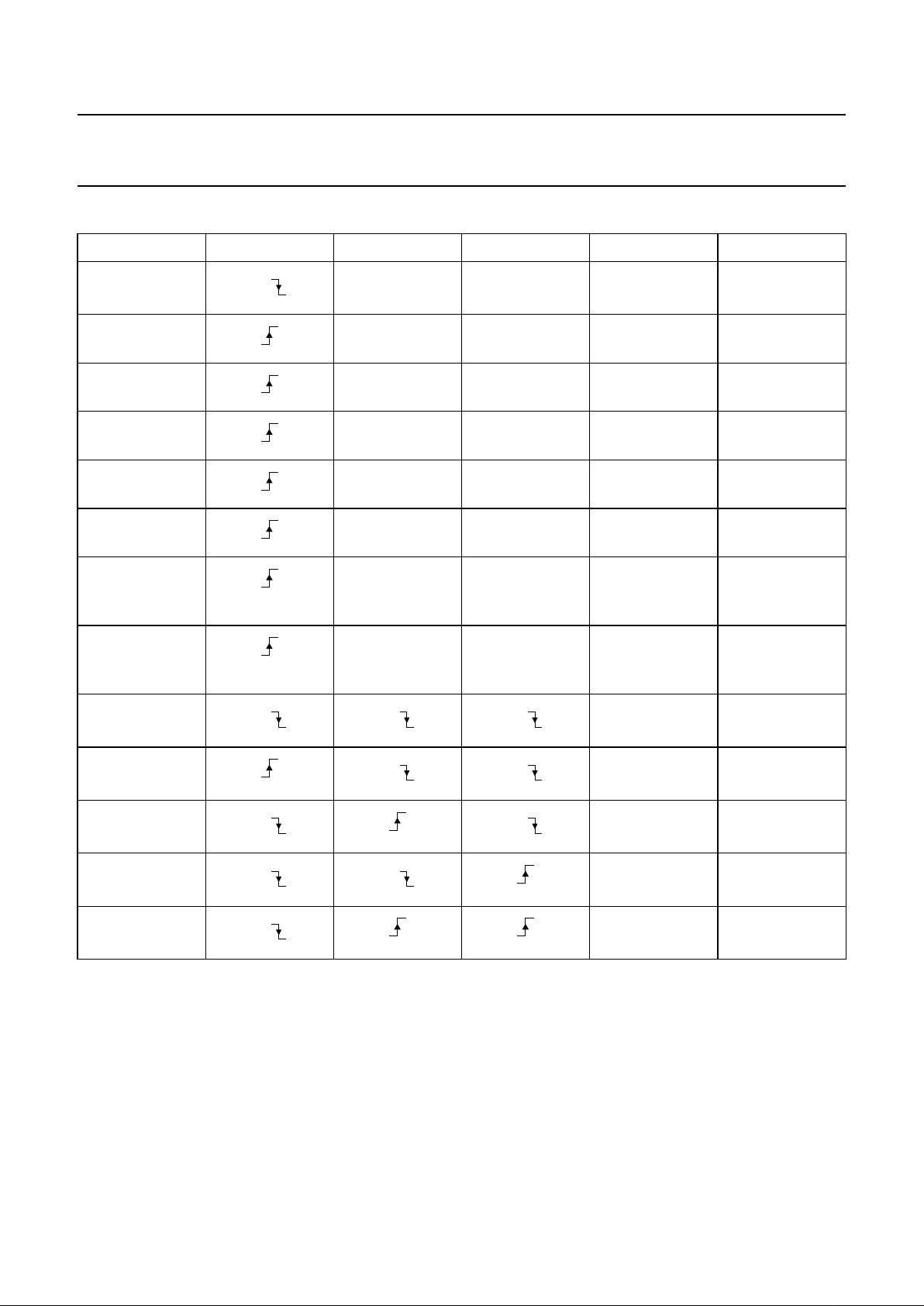
Serial Interface
DIGITAL INPUTS (SEN1, SEN2, SCLK, SDATA AND SMODE)
V
IL
LOW-level input voltage 0 − 0.8 V
V
IH
HIGH-level input voltage 2.0 − V
DDD
V
I
IH
HIGH-level input current −50 +5µA
I
IL
LOW-level input current −50 +5µA
GAIN CONTROL DATA TIMING (see Fig.4)
f
SCLK(max)
maximum clock frequency 5 −−MHz
t
W(SCLKH)
clock pulse width HIGH 20 −−ns
t
W(SCLKL)
clock pulse width LOW 20 −−ns
t
su(SEN-SCLK
) SEN to SCLK set-up time 5 −−ns
t
h(SEN-SCLK)
SEN to SCLK hold time 5 −−ns
t
su(SDATA-SCLK)
SDATA to SCLK set-up time 5 −−ns
t
h(SMODE-SCLK)
SMODE to SCLK hold time 5 −−ns
t
h(SMODE-SEN)
SMODE to SEN hold time 5 −−ns
t
d(SEN-Q)
delay SEN rising edge to
change gain control register
value
−− 5ns
t
d(SCLK-Q)
delay SCLK rising edge to
change gain control register
value
−− 5ns
SYMBOL PARAMETER CONDITIONS MIN. TYP. MAX. UNIT
Page 15

1999 Sep 16 15
Philips Semiconductors Objective specification
Dual 8-bit, 100 Msps A/D converter with
DPGA
TDA8798
This text is here in white to force landscape pages to be rotated correctly when browsing through the pdf in the Acrobat reader.This text is here in
_white to force landscape pages to be rotated correctly when browsing through the pdf in the Acrobat reader.This text is here inThis text is here in
white to force landscape pages to be rotated correctly when browsing through the pdf in the Acrobat reader. white to force landscape pages to be ...
handbook, full pagewidth
MGM865
SI GAIN
CONTROL
REGISTER
DPGA
OUTPUTS
SDATA
SCLK
SEN
SMODE
D5
(MSB) (LSB)
D4 D3 D2 D1 D0
up = 1
down = 0
up = 1
down = 0
t
h(SMODE-SEN)
t
su(SEN-SCLK)
t
su(SDATA-SCLK)
t
W(SCLKH)
t
h(SMODE-SCLK)
t
W(SCLKL)
t
h(SEN-SCLK)
t
su(SEN-SCLK)
t
su(SEN-SCLK)
t
d(SCLK-Q)
t
d(SEN-Q)
t
st(G-G)
t
PD
50%
10%
90%
50%
50%
D5 D4 D3 D2 D1 D0 REG +/−1 REG +/−1
parallel load mode count-up/count-down mode
Fig.4 Timing diagram of serial interface.
Page 16

1999 Sep 16 16
Philips Semiconductors Objective specification
Dual 8-bit, 100 Msps A/D converter with
DPGA
TDA8798
Fig.5 Timing diagram for the ADC.
handbook, full pagewidth
t
d(s)(D)
CLK
MGM866
50 %
HIGH
LOW
50 %
HIGH
LOW
sample N
sample N + 1 sample N + 2
V
i
DATA
A0 to A7
B0 to B7
t
h(Q)
t
d(Q)
t
W(CLKH)
t
W(CLKL)
DATA
N − 1
DATA
N − 2
DATA
N + 1
DATA
N
Fig.6 Timing diagram and test conditions of 3-state output delay time.
handbook, full pagewidth
tdLZ
t
dZL
V
DDO
0 V
data
output
data
output
OE
OE
50%
10%
A0 to A7
B0 to B7
tdHZ
t
dZH
high impedance
high impedance
logic LOW
50%
50%
90%
MGM868
TEST S1
S1
3.3 kΩ
10 pF
t
dLZ
V
DDO
V
DDO
t
dZL
V
DDO
t
dHZ
GND
t
dZH
GND
TDA8798
logic HIGH
Page 17

1999 Sep 16 17
Philips Semiconductors Objective specification
Dual 8-bit, 100 Msps A/D converter with
DPGA
TDA8798
TEST AND APPLICATION INFORMATION
Fig.7 Application diagram.
handbook, full pagewidth
100 nF
(1)
TDA8798HL
MGM867
1
2
3
4
5
6
7
8
9
10
11
12
13
14
15
16
48
47
46
45
44
43
42
41
40
39
38
37
36
35
34
33
3.3 V3.3 V3.3 V
B7
B6
B5
B4
B3
B2
B1
B0
A0
A1
A2
A3
A4
A5
A6
A7
B7
B6
B5
B4
B3
B2
B1
B0
A0
A1
A2
A3
A4
A5
A6
A7
DPGA2N
DPGA2
DPGAC2
V
ref2
V
ref1
V
DDA2
VIN2N
VIN2
V
IN2N
V
IN2
V
SSA2
V
SSA1
VIN1
VIN1N
V
IN1
V
IN1N
V
DDA1
DPGAC1
DPGA1
DPGA1N
17
18
19
20
21
22
23
24
25
26
27
28
29
30
31
32
64
63
62
61
60
59
58
57
56
55
54
53
52
51
50
49
BUF2
BUF2N
V
oref2
V
DDA4
V
SSA4
CLK2N
CLK2
CLK2
V
SSD2
V
DDD2
SR
V
DDO2
V
SSO2
BUF1
BUF1N
V
oref1
V
DDA3
V
SSA3
CLK1N
CLK1
CLK1
V
SSD1
V
DDD1
SMODE
SEN2
SDATA
SCLK
SEN1
SMODE
SEN2
SDATA
SCLK
SEN1
V
DDO1
V
SSO1
V
SSO
V
SSO
V
SSD
V
SSD
V
SSA
V
SSA
TE
OE
TE
OE
V
SSD
V
SSO
V
SSD
V
SSA
SR
TEST
V
SSD
DPGAEN
DPGAEN
100 nF
(1)
3.3 V
V
SSO
100 nF
(1)
3.3 V
V
SSD
100 nF
(1)
3.3 V
V
SSA
100 nF
(1)
100 nF
(1)
100 nF
(2)
68 pF
(3)
68 pF
(3)
100 nF
(4)
100 nF
(2)
100 nF
(2)
100 nF
(2)
100 nF
100 nF
100 nF
(4)
100 nF
(4)
100 nF
(4)
3.3 V
V
SSA
V
SSA
100 nF
(1)
3.3 V
V
SSA
V
SSA
100 nF
(1)
V
SSD
Analog and digital supplies must be separate and decoupled.
(1) Supply decoupling capacitor must be placed as close as possible to the chip’s pin. Value may need changing depending on the external filter
characteristics.
(2) Capacitor may be replaced when an external filter is used with AC coupling.
(3) Capacitor value may be changed to adjust settling time between DPGA gain changes.
(4) Capacitor value may need changing depending on the high-pass cut-off frequency of the external filter.
Page 18

1999 Sep 16 18
Philips Semiconductors Objective specification
Dual 8-bit, 100 Msps A/D converter with
DPGA
TDA8798
INTERNAL PIN CONFIGURATIONS
handbook, halfpage
MGM869
1 kΩ
0.5 V
V
SSA1
V
DDA1
VIN1
VIN1N
Fig.8 DPGA1 analog input.
handbook, halfpage
MGM870
1 kΩ
0.5 V
V
SSA2
V
DDA2
VIN2
VIN2N
Fig.9 DPGA2 analog input.
Fig.10 ADC1 buffer input and V
oref1
output.
handbook, halfpage
MGM871
20
kΩ
0.42 V
V
SSA3
V
DDA3
V
oref1
BUF1
BUF1N
Fig.11 ADC2 buffer input and V
oref2
output.
handbook, halfpage
MGM872
20
kΩ
0.42 V
V
SSA4
V
DDA4
V
oref2
BUF2
BUF2N
Fig.12 ADC1 clock buffer input.
handbook, halfpage
MGM873
20
kΩ
V
SSD1
V
DDD1
CLK1
CLK1N
1.4 V
Fig.13 ADC2 clock buffer input.
handbook, halfpage
MGM874
20
kΩ
V
SSD2
V
DDD2
CLK2
CLK2N
1.4 V
Page 19

1999 Sep 16 19
Philips Semiconductors Objective specification
Dual 8-bit, 100 Msps A/D converter with
DPGA
TDA8798
handbook, halfpage
MGM875
100 Ω
V
SSA1
V
DDA3
V
DDA1
DPGA1
DPGA1N
Fig.14 DPGA1 buffer output.
handbook, halfpage
MGM876
100 Ω
V
SSA2
V
DDA4
V
DDA2
DPGA2
DPGA2N
Fig.15 DPGA2 buffer output.
Fig.16 Serial Interface inputs.
handbook, halfpage
MGM877
V
DDD1
SMODE
SEN1
SEN2
SDATA
SCLK
V
SSD1
Fig.17 TE and DPGAEN inputs.
handbook, halfpage
MGM878
V
DDD2
TE
DPGAEN
V
SSD2
Fig.18 OE and SR inputs.
handbook, halfpage
MGM879
V
DDO2
OE
SR
V
SSO2
handbook, halfpage
MGM880
V
DDO1
A0N
OE
A0
V
SSO1
Fig.19 ADC1 A0 to A7 outputs.
Page 20

1999 Sep 16 20
Philips Semiconductors Objective specification
Dual 8-bit, 100 Msps A/D converter with
DPGA
TDA8798
handbook, halfpage
MGM881
V
DDO2
B0N
OE
B0
V
SSO2
Fig.20 ADC2 B0 to B7 outputs. Fig.21 V
ref1
output.
FCE268
V
DDA3
V
ref1
V
SSA3
1.24 V
Fig.22 V
ref2
output.
FCE269
V
DDA4
V
ref2
1.24 V
V
SSA4
Page 21

1999 Sep 16 21
Philips Semiconductors Objective specification
Dual 8-bit, 100 Msps A/D converter with
DPGA
TDA8798
PACKAGE OUTLINE
UNIT
A
max.
A1A2A3b
p
cE
(1)
eH
E
LL
p
Zywv θ
REFERENCES
OUTLINE
VERSION
EUROPEAN
PROJECTION
ISSUE DATE
IEC JEDEC EIAJ
mm
1.60
0.20
0.05
1.45
1.35
0.25
0.27
0.17
0.18
0.12
10.1
9.9
0.5
12.15
11.85
1.45
1.05
7
0
o
o
0.12 0.11.0 0.2
DIMENSIONS (mm are the original dimensions)
Note
1. Plastic or metal protrusions of 0.25 mm maximum per side are not included.
0.75
0.45
SOT314-2
95-12-19
97-08-01
D
(1) (1)(1)
10.1
9.9
H
D
12.15
11.85
E
Z
1.45
1.05
D
b
p
e
θ
E
A
1
A
L
p
detail X
L
(A )
3
B
16
c
D
H
b
p
E
H
A
2
v M
B
D
Z
D
A
Z
E
e
v M
A
X
1
64
49
48 33
32
17
y
pin 1 index
w M
w M
0 2.5 5 mm
scale
LQFP64: plastic low profile quad flat package; 64 leads; body 10 x 10 x 1.4 mm
SOT314-2
Page 22

1999 Sep 16 22
Philips Semiconductors Objective specification
Dual 8-bit, 100 Msps A/D converter with
DPGA
TDA8798
SOLDERING
Introduction to soldering surface mount packages
Thistextgivesavery brief insight to a complex technology.
A more in-depth account of soldering ICs can be found in
our
“Data Handbook IC26; Integrated Circuit Packages”
(document order number 9398 652 90011).
There is no soldering method that is ideal for all surface
mount IC packages. Wavesoldering is not always suitable
for surface mount ICs, or for printed-circuit boards with
high population densities. In these situations reflow
soldering is often used.
Reflow soldering
Reflow soldering requires solder paste (a suspension of
fine solder particles, flux and binding agent) to be applied
tothe printed-circuit board by screen printing,stencillingor
pressure-syringe dispensing before package placement.
Several methods exist for reflowing; for example,
infrared/convection heating in a conveyor type oven.
Throughput times (preheating, soldering and cooling) vary
between 100 and 200 seconds depending on heating
method.
Typical reflow peak temperatures range from
215 to 250 °C. The top-surface temperature of the
packages should preferable be kept below 230 °C.
Wave soldering
Conventional single wave soldering is not recommended
forsurfacemountdevices(SMDs)orprinted-circuit boards
with a high component density, as solder bridging and
non-wetting can present major problems.
To overcome these problems the double-wave soldering
method was specifically developed.
If wave soldering is used the following conditions must be
observed for optimal results:
• Use a double-wave soldering method comprising a
turbulent wave with high upward pressure followed by a
smooth laminar wave.
• For packages with leads on two sides and a pitch (e):
– larger than or equal to 1.27 mm, the footprint
longitudinal axis is preferred to be parallel to the
transport direction of the printed-circuit board;
– smaller than 1.27 mm, the footprint longitudinal axis
must be parallel to the transport direction of the
printed-circuit board.
The footprint must incorporate solder thieves at the
downstream end.
• Forpackageswithleadsonfoursides,the footprint must
be placed at a 45° angle to the transport direction of the
printed-circuit board. The footprint must incorporate
solder thieves downstream and at the side corners.
During placement and before soldering, the package must
be fixed with a droplet of adhesive. The adhesive can be
applied by screen printing, pin transfer or syringe
dispensing. The package can be soldered after the
adhesive is cured.
Typical dwell time is 4 seconds at 250 °C.
A mildly-activated flux will eliminate the need for removal
of corrosive residues in most applications.
Manual soldering
Fix the component by first soldering two
diagonally-opposite end leads. Use a low voltage (24 V or
less) soldering iron applied to the flat part of the lead.
Contact time must be limited to 10 seconds at up to
300 °C.
When using a dedicated tool, all other leads can be
soldered in one operation within 2 to 5 seconds between
270 and 320 °C.
Page 23

1999 Sep 16 23
Philips Semiconductors Objective specification
Dual 8-bit, 100 Msps A/D converter with
DPGA
TDA8798
Suitability of surface mount IC packages for wave and reflow soldering methods
Notes
1. All surface mount (SMD) packages are moisture sensitive. Depending upon the moisture content, the maximum
temperature (with respect to time) and body size of the package, there is a risk that internal or external package
cracks may occur due to vaporization of the moisture in them (the so called popcorn effect). For details, refer to the
Drypack information in the
“Data Handbook IC26; Integrated Circuit Packages; Section: Packing Methods”
.
2. These packages are not suitable for wave soldering as a solder joint between the printed-circuit board and heatsink
(at bottom version) can not be achieved, and as solder may stick to the heatsink (on top version).
3. If wave soldering is considered, then the package must be placed at a 45° angle to the solder wave direction.
The package footprint must incorporate solder thieves downstream and at the side corners.
4. Wave soldering is only suitable for LQFP, TQFP and QFP packages with a pitch (e) equal to or larger than 0.8 mm;
it is definitely not suitable for packages with a pitch (e) equal to or smaller than 0.65 mm.
5. Wave soldering is only suitable for SSOP and TSSOP packages with a pitch (e) equal to or larger than 0.65 mm; it is
definitely not suitable for packages with a pitch (e) equal to or smaller than 0.5 mm.
DEFINITIONS
LIFE SUPPORT APPLICATIONS
These products are not designed for use in life support appliances, devices, or systems where malfunction of these
products can reasonably be expected to result in personal injury. Philips customers using or selling these products for
use in such applications do so at their own risk and agree to fully indemnify Philips for any damages resulting from such
improper use or sale.
PACKAGE
SOLDERING METHOD
WAVE REFLOW
(1)
BGA, SQFP not suitable suitable
HLQFP, HSQFP, HSOP, HTSSOP, SMS not suitable
(2)
suitable
PLCC
(3)
, SO, SOJ suitable suitable
LQFP, QFP, TQFP not recommended
(3)(4)
suitable
SSOP, TSSOP, VSO not recommended
(5)
suitable
Data sheet status
Objective specification This data sheet contains target or goal specifications for product development.
Preliminary specification This data sheet contains preliminary data; supplementary data may be published later.
Product specification This data sheet contains final product specifications.
Limiting values
Limiting values given are in accordance with the Absolute Maximum Rating System (IEC 134). Stress above one or
more of the limiting values may cause permanent damage to the device. These are stress ratings only and operation
of the device at these or at any other conditions above those given in the Characteristics sections of the specification
is not implied. Exposure to limiting values for extended periods may affect device reliability.
Application information
Where application information is given, it is advisory and does not form part of the specification.
Page 24

© Philips Electronics N.V. SCA
All rights are reserved. Reproduction in whole or in part is prohibited without the prior written consent of the copyright owner.
The information presented in this document does not form part of any quotation or contract, is believed to be accurate and reliable and may be changed
without notice. No liability will be accepted by the publisher for any consequence of its use. Publication thereof does not convey nor imply any license
under patent- or other industrial or intellectual property rights.
Internet: http://www.semiconductors.philips.com
1999
68
Philips Semiconductors – a w orldwide compan y
For all other countries apply to: Philips Semiconductors,
International Marketing & Sales Communications, Building BE-p, P.O. Box 218,
5600 MD EINDHOVEN, The Netherlands, Fax. +31 40 27 24825
Argentina: see South America
Australia: 3 Figtree Drive, HOMEBUSH, NSW 2140,
Tel. +61 2 9704 8141, Fax. +61 2 9704 8139
Austria: Computerstr. 6, A-1101 WIEN, P.O. Box 213,
Tel. +43 1 60 101 1248, Fax. +43 1 60 101 1210
Belarus: Hotel Minsk Business Center, Bld. 3, r. 1211, Volodarski Str. 6,
220050 MINSK, Tel. +375 172 20 0733, Fax. +375 172 20 0773
Belgium: see The Netherlands
Brazil: see South America
Bulgaria: Philips Bulgaria Ltd., Energoproject, 15th floor,
51 James Bourchier Blvd., 1407 SOFIA,
Tel. +359 2 68 9211, Fax. +359 2 68 9102
Canada: PHILIPS SEMICONDUCTORS/COMPONENTS,
Tel. +1 800 234 7381, Fax. +1 800 943 0087
China/Hong Kong: 501 Hong Kong Industrial Technology Centre,
72 Tat Chee Avenue, Kowloon Tong, HONG KONG,
Tel. +852 2319 7888, Fax. +852 2319 7700
Colombia: see South America
Czech Republic: see Austria
Denmark: Sydhavnsgade 23, 1780 COPENHAGEN V,
Tel. +45 33 29 3333, Fax. +45 33 29 3905
Finland: Sinikalliontie 3, FIN-02630 ESPOO,
Tel. +358 9 615 800, Fax. +358 9 6158 0920
France: 51 Rue Carnot, BP317, 92156 SURESNES Cedex,
Tel. +33 1 4099 6161, Fax. +33 1 4099 6427
Germany: Hammerbrookstraße 69, D-20097 HAMBURG,
Tel. +49 40 2353 60, Fax. +49 40 2353 6300
Hungary: see Austria
India: Philips INDIA Ltd, Band Box Building, 2nd floor,
254-D, Dr. Annie Besant Road, Worli, MUMBAI 400 025,
Tel. +91 22 493 8541, Fax. +91 22 493 0966
Indonesia: PT Philips Development Corporation, Semiconductors Division,
Gedung Philips, Jl. Buncit Raya Kav.99-100, JAKARTA 12510,
Tel. +62 21 794 0040 ext. 2501, Fax. +62 21 794 0080
Ireland: Newstead, Clonskeagh, DUBLIN 14,
Tel. +353 1 7640 000, Fax. +353 1 7640 200
Israel: RAPAC Electronics, 7 Kehilat Saloniki St, PO Box 18053,
TEL AVIV 61180, Tel. +972 3 645 0444, Fax. +972 3 649 1007
Italy: PHILIPS SEMICONDUCTORS, Via Casati, 23 - 20052 MONZA (MI),
Tel. +39 039 203 6838, Fax +39 039 203 6800
Japan: Philips Bldg 13-37, Kohnan 2-chome, Minato-ku,
TOKYO 108-8507, Tel. +81 3 3740 5130, Fax. +81 3 3740 5057
Korea: Philips House, 260-199 Itaewon-dong, Yongsan-ku, SEOUL,
Tel. +82 2 709 1412, Fax. +82 2 709 1415
Malaysia: No. 76 Jalan Universiti, 46200 PETALING JAYA, SELANGOR,
Tel. +60 3 750 5214, Fax. +60 3 757 4880
Mexico: 5900 Gateway East, Suite 200, EL PASO, TEXAS 79905,
Tel. +9-5 800 234 7381, Fax +9-5 800 943 0087
Middle East: see Italy
Netherlands: Postbus 90050, 5600 PB EINDHOVEN, Bldg. VB,
Tel. +31 40 27 82785, Fax. +31 40 27 88399
New Zealand: 2 Wagener Place, C.P.O. Box 1041, AUCKLAND,
Tel. +64 9 849 4160, Fax. +64 9 849 7811
Norway: Box 1, Manglerud 0612, OSLO,
Tel. +47 22 74 8000, Fax. +47 22 74 8341
Pakistan: see Singapore
Philippines: Philips Semiconductors Philippines Inc.,
106 Valero St. Salcedo Village, P.O. Box 2108 MCC, MAKATI,
Metro MANILA, Tel. +63 2 816 6380, Fax. +63 2 817 3474
Poland: Al.Jerozolimskie 195 B, 02-222 WARSAW,
Tel. +48 22 5710 000, Fax. +48 22 5710 001
Portugal: see Spain
Romania: see Italy
Russia: Philips Russia, Ul. Usatcheva 35A, 119048 MOSCOW,
Tel. +7 095 755 6918, Fax. +7 095 755 6919
Singapore: Lorong 1, Toa Payoh, SINGAPORE 319762,
Tel. +65 350 2538, Fax. +65 251 6500
Slovakia: see Austria
Slovenia: see Italy
South Africa: S.A. PHILIPS Pty Ltd., 195-215 Main Road Martindale,
2092 JOHANNESBURG, P.O. Box 58088 Newville 2114,
Tel. +27 11 471 5401, Fax. +27 11 471 5398
South America: Al. Vicente Pinzon, 173, 6th floor,
04547-130 SÃO PAULO, SP, Brazil,
Tel. +55 11 821 2333, Fax. +55 11 821 2382
Spain: Balmes 22, 08007 BARCELONA,
Tel. +34 93 301 6312, Fax. +34 93 301 4107
Sweden: Kottbygatan 7, Akalla, S-16485 STOCKHOLM,
Tel. +46 8 5985 2000, Fax. +46 8 5985 2745
Switzerland: Allmendstrasse 140, CH-8027 ZÜRICH,
Tel. +41 1 488 2741 Fax. +41 1 488 3263
Taiwan: Philips Semiconductors, 6F, No. 96, Chien Kuo N. Rd., Sec. 1,
TAIPEI, Taiwan Tel. +886 2 2134 2886, Fax. +886 2 2134 2874
Thailand: PHILIPS ELECTRONICS (THAILAND) Ltd.,
209/2 Sanpavuth-Bangna Road Prakanong, BANGKOK 10260,
Tel. +66 2 745 4090, Fax. +66 2 398 0793
Turkey: Yukari Dudullu, Org. San. Blg., 2.Cad. Nr. 28 81260 Umraniye,
ISTANBUL, Tel. +90 216 522 1500, Fax. +90 216 522 1813
Ukraine: PHILIPS UKRAINE, 4 Patrice Lumumba str., Building B, Floor 7,
252042 KIEV, Tel. +380 44 264 2776, Fax. +380 44 268 0461
United Kingdom: Philips Semiconductors Ltd., 276 Bath Road, Hayes,
MIDDLESEX UB3 5BX, Tel. +44 208 730 5000, Fax. +44 208 754 8421
United States: 811 East Arques Avenue, SUNNYVALE, CA 94088-3409,
Tel. +1 800 234 7381, Fax. +1 800 943 0087
Uruguay: see South America
Vietnam: see Singapore
Yugoslavia: PHILIPS, Trg N. Pasica 5/v, 11000 BEOGRAD,
Tel. +381 11 62 5344, Fax.+381 11 63 5777
Printed in The Netherlands 545004/25/02/pp24 Date of release: 1999 Sep 16 Document order number: 9397 750 05466
 Loading...