

Page 1

INTEGRATED CIRCUITS
DATA SH EET
TDA8793
8-bit, low-power, 3 V, 100 Msps
Analog-to-Digital Converter (ADC)
Product specification
Supersedes data of 1999 Oct 06
File under Integrated Circuits, IC02
2000 Nov 20
Page 2
Philips Semiconductors Product specification
8-bit, low-power, 3 V, 100 Msps
Analog-to-Digital Converter (ADC)
FEATURES
• 8-bit low-power ADC: 180 mW (typical value)
• 2.7 to 3.6 V operation
• Track-and-hold circuit
• In track-and-hold mode: sampling rate from
70 to 100 Msps
• In non track-and-hold mode: sampling rate from
1 sps to 100 Msps
• CMOS/TTL compatible digital inputs and outputs
• Internal reference voltages
• Adjustable full-scale range possibility with external
reference
• Power-down mode: 5 mW.
APPLICATIONS
• Radio communications
• Digital data storage read channels
• Medical imaging
• Digital instrumentation.
TDA8793
GENERAL DESCRIPTION
The TDA8793 is an 8-bit low-power Analog-to-Digital
Converter (ADC) which includes a track-and-hold circuit
and internal references. The device converts an analog
input signal, up to 100 MHz, into 8-bit binary codes at a
maximum sample rate of 100 Msps. All digital inputs and
outputs are CMOS/TTL compatible. A sine wave clock
input signal can also be used.
The Power-down mode enables the device power
consumption to be reduced to 5 mW.
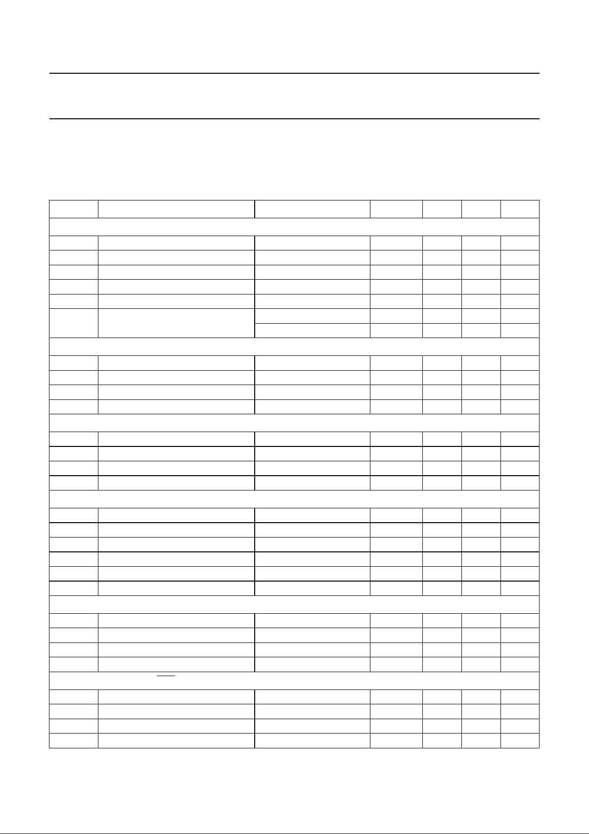
QUICK REFERENCE DATA
SYMBOL PARAMETER CONDITIONS MIN. TYP. MAX. UNIT
V
V
V
I
CCA
CCA
CCD
CCO
analog supply voltage 2.7 3.0 3.6 V
digital supply voltage 2.7 3.0 3.6 V
output stages supply voltage 2.7 3.0 3.6 V
analog supply current operating 32 40 48 mA
standby 0 2 100 µA
I
CCD
digital supply current operating 12 16 24 mA
standby 0 0.66 1.1 mA
I
CCO
INL integral non-linearity ramp input; f
DNL differential non-linearity ramp input; f
f
CLK(max)
P
tot
output stages supply current ramp input − 4 6.5 mA
V
CCA=VCCD
V
CCA=VCCD
CLK
=3V
CLK
=3V
= 2 MHz;
= 2 MHz;
−±0.85 ±1.70 LSB
−±0.25 ±0.80 LSB
maximum clock input frequency 100 −−MHz
total power dissipation VCC=3V − 180 − mW
ORDERING INFORMATION
TYPE
NUMBER
NAME DESCRIPTION VERSION
PACKAGE
TDA8793HL LQFP32 plastic low profile quad flat package; 32 leads; body 5 × 5 × 1.4 mm SOT401-1
2000 Nov 20 2
Page 3
Philips Semiconductors Product specification
8-bit, low-power, 3 V, 100 Msps
Analog-to-Digital Converter (ADC)
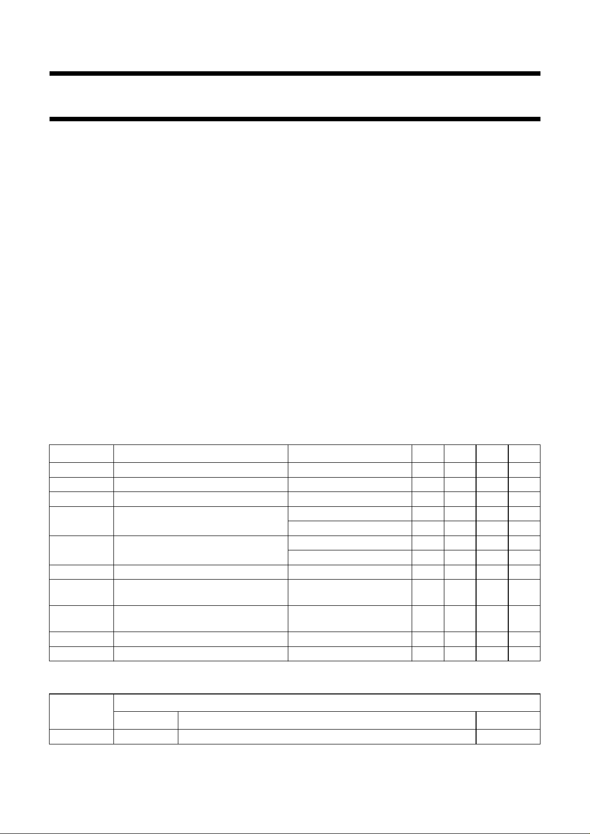
BLOCK DIAGRAM
handbook, full pagewidth
INP
INN
REFOUT
REFIN
4
3
5
2
TEN
12
TRACK-AND-
HOLD
V
CCA
TDA8793
V
7
V
CCD
CCO2
10
ADC
CLOCK DRIVER
V
22
LATCHES
CCO1
20
CMOS
OUTPUTS
26
D7
25
D6
24
D5
23
D4
18
D3
17
D2
16
D1
15
D0
11
CLK
SDN
STDBY
32
8
REFERENCE
VOLTAGES
31
DEC
TDA8793
6
AGND
9
DGND
Fig.1 Block diagram.
21
OGND119OGND2
MGR016
2000 Nov 20 3
Page 4
Philips Semiconductors Product specification
8-bit, low-power, 3 V, 100 Msps
Analog-to-Digital Converter (ADC)
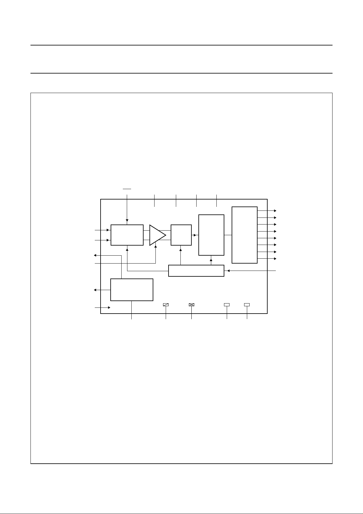
PINNING
SYMBOL PIN DESCRIPTION
n.c. 1 not connected
REFIN 2 reference input for ADC
INN 3 negative input
INP 4 positive input
REFOUT 5 reference output for AC coupling of
input
AGND 6 analog ground
V
CCA
STDBY 8 standby mode input
DGND 9 digital ground
V
CCD
CLK 11 clock input
TEN 12 track enable input (active LOW)
n.c. 13 not connected
n.c. 14 not connected
D0 15 data output bit 0 (LSB)
D1 16 data output bit 1
7 analog supply voltage
10 digital supply voltage
TDA8793
SYMBOL PIN DESCRIPTION
D2 17 data output bit 2
D3 18 data output bit 3
OGND1 19 output ground 1
V
CCO1
OGND2 21 output ground 2
V
CCO2
D4 23 data output bit 4
D5 24 data output bit 5
D6 25 data output bit 6
D7 26 data output bit 7 (MSB)
n.c. 27 not connected
n.c. 28 not connected
n.c. 29 not connected
n.c. 30 not connected
DEC 31 decoupling
SDN 32 stabilized decoupling node output
20 output supply voltage 1
22 output supply voltage 2
handbook, full pagewidth
n.c.
REFIN
INN
INP
1
2
3
4
SDN
32
DEC
31
n.c.
30
n.c.
29
TDA8793
AGND
V
CCA
5
6
7
8
9
DGND
10
CCD
V
11
CLK
12
TEN
REFOUT
STDBY
Fig.2 Pin configuration.
2000 Nov 20 4
n.c.
28
13
n.c.
n.c.
27
14
n.c.
D7
26
15
D0
D6
25
16
D1
24
23
22
21
20
19
18
17
MGR017
D5
D4
V
CCO2
OGND2
V
CCO1
OGND1
D3
D2
Page 5
Philips Semiconductors Product specification
8-bit, low-power, 3 V, 100 Msps
TDA8793
Analog-to-Digital Converter (ADC)
LIMITING VALUES
In accordance with the Absolute Maximum Rating System (IEC 60134).
SYMBOL PARAMETER CONDITIONS MIN. MAX. UNIT
V
V
V
∆V
V
I
O
T
T
CCA
CCD
CCO
CC
n
stg
amb
analog supply voltage note 1 −0.3 +5.0 V
digital supply voltage note 1 −0.3 +5.0 V
output stages supply voltage note 1 −0.3 +5.0 V
supply voltage differences between
V
V
V
CCA
CCO
CCA
and V
and V
and V
CCD
CCD
CCO
−1.0 +1.0 V
−1.0 +1.0 V
−1.0 +1.0 V
voltage on pins
INP, INN, CLK,
TEN and STDBY note 2 −0.3 +4.5 V
REFIN −0.3 +4.5 V
output current − 10 mA
storage temperature −55 +150 °C
ambient temperature 0 70 °C
Notes
1. The supply voltages V
CCA
, V
CCD
, V
may have any value between −0.3 and +5.0 V provided that the supply
CCO
voltage differences ∆VCC are respected.
2. All voltages are typical values and are referenced to all ground pins connected together.
HANDLING
Inputs and outputs are protected against electrostatic discharges in normal handling. However, to be totally safe, it is
desirable to take normal precautions appropriate to handling integrated circuits.
THERMAL CHARACTERISTICS
SYMBOL PARAMETER CONDITIONS VALUE UNIT
R
th(j-a)
thermal resistance from junction to ambient in free air 94 K/W
2000 Nov 20 5
Page 6
Philips Semiconductors Product specification
8-bit, low-power, 3 V, 100 Msps
TDA8793
Analog-to-Digital Converter (ADC)
CHARACTERISTICS
V
CCA=V7
DGND and OGND shorted together; V
V
CCA
T
amb
SYMBOL PARAMETER CONDITIONS MIN. TYP. MAX. UNIT
Supplies
V
CCA
V
CCD
V
CCO
I
CCA
I
CCD
I
CCO
Internal reference voltage output (pin SDN); note 1
V
ref
V
reg
TC temperature coefficient − 20 − ppm/K
I
L
Internal reference voltage output (pin REFOUT)
V
ref
V
reg
TC temperature coefficient − 20 − ppm/K
I
L
Clock input (pin CLK); note 2
V
IL
V
IH
I
IL
I
IH
Z
i
C
i
Standby input (pin STDBY); see Table 1
V
IL
V
IH
I
IL
I
IH
Track enable input (pin TEN); see Table 2
V
IL
V
IH
I
IL
I
IH
to V6= 2.7 to 3.6 V; V
to V
= −0.15 to +0.15 V; T
CCO
CCD=V10
amb
to V9= 2.7 to 3.6 V; V
CCA
to V
= −0.15 to +0.15 V; V
CCD
= 0 to 70 °C; typical values measured at V
=25°C; single-ended input; unless otherwise specified.
analog supply voltage 2.7 3.0 3.6 V
digital supply voltage 2.7 3.0 3.6 V
output stages supply voltage 2.7 3.0 3.6 V
analog supply current 32 40 48 mA
digital supply current 12 16 24 mA
output stages supply current ramp input − 4 6.5 mA
f
= 20 MHz − 8.7 12 mA
i
reference voltage 1.21 1.26 1.31 V
line regulation voltage 2.7 < V
CCA
load current −1 −−mA
reference voltage 1.76 1.84 1.92 V
line regulation voltage 2.7 < V
CCA
load current −1 −−mA
LOW-level input voltage 0 − 0.8 V
HIGH-level input voltage 2 − V
LOW-level input current V
HIGH-level input current V
input impedance f
input capacitance f
=0 −2 − +2 µA
CLK
CLK=VCCD
= 100 MHz − 32 − kΩ
CLK
= 100 MHz − 2 − pF
CLK
LOW-level input voltage 0 − 0.8 V
HIGH-level input voltage 2 − V
LOW-level input current V
HIGH-level input current V
=0 −5 −−µA
STDBY
STDBY=VCCD
LOW-level input voltage 0 − 0.8 V
HIGH-level input voltage 2 − V
LOW-level input current V
HIGH-level input current V
=0 −5 −−µA
TEN
TEN=VCCD
CCO=V20
to V19 and V22to V21= 2.7 to 3.6 V; AGND,
CCD
to V
= −0.15 to +0.15 V;
CCO
CCA=VCCD=VCCO
= 3.0 V and
< 3.6 V − 1.25 4 mV
< 3.6 V − 1.5 5 mV
CCD
V
−−5µA
CCD
V
−−5µA
CCD
V
−−5µA
2000 Nov 20 6
Page 7

Philips Semiconductors Product specification
8-bit, low-power, 3 V, 100 Msps
TDA8793
Analog-to-Digital Converter (ADC)
SYMBOL PARAMETER CONDITIONS MIN. TYP. MAX. UNIT
Analog inputs (pins INP and INN); input voltage referenced to AGND; V
V
∆V
i(p-p)
i(T)
input voltage range
(peak-to-peak value)
input voltage range variation with
Vi=V
T
amb
− V
INP
=25°C
INN
;
temperature
V
IO
Z
i
C
i
I
I
input offset voltage output code = 127 −30 − +30 mV
input impedance fi= 50 MHz − 90 − kΩ
input capacitance fi= 50 MHz − 2 − pF
input current VI=V
V
I=VREFOUT
REFOUT
− 0.5 V −1 −−µA
+ 0.5 V −−40 µA
Adjustable full-scale range
V
i(p-p)
input voltage range
(peak-to-peak value)
Vi=V
V
REFIN
T
amb
− V
INP
= 1.27 V;
=25°C; see Fig.3
INN
;
Reference input for ADC (pin REFIN); referenced to AGND; note 3
V
REFIN
I
REFIN
reference input voltage 1.25 1.27 1.35 V
reference input current − 0.9 1.1 mA
ADC data outputs (pins D0 to D7)
V
OL
V
OH
C
L
δV/δt slew rate 20% to 80%; C
LOW-level output voltage IO=1mA −−0.54 V
I
= 0.6 mA −−0.40 V
O
HIGH-level output voltage IO= −0.4 mA V
load capacitance −−10 pF
=10pF − 1.6 − V/ns
L
Analog signal processing; see Figs 4, 5, 6 and 7; note 3
INL integral non-linearity ramp input; f
V
CCA=VCCD
DNL differential non-linearity ramp input; f
V
CCA=VCCD
CLK
=3V
CLK
=3V
= 2 MHz;
= 2 MHz;
S/N signal-to-noise ratio (full-scale) without harmonics;
= 100 MHz:
f
CLK
= 20 MHz 43 48 − dB
f
i
f
= 50 MHz − 47 − dB
i
B −3 dB analog bandwidth track-and-hold active − 350 − MHz
THD total harmonic distortion f
H
fund(FS)
fundamental harmonics (full-scale) f
= 20 MHz −−53 − dB
i
f
= 50 MHz −−51 − dB
i
= 100 MHz:
CLK
f
= 20 MHz −−0dB
i
f
= 50 MHz −−0dB
i
= 1.27 V; see Table 3
REFIN
0.90 0.95 1.02 V
− 0.5 − mV/K
− 1 − V
− 0.5 − V
CCO
CCO
−±0.85 ±1.70 LSB
−±0.25 ±0.80 LSB
V
2000 Nov 20 7
Page 8

Philips Semiconductors Product specification
8-bit, low-power, 3 V, 100 Msps
TDA8793
Analog-to-Digital Converter (ADC)
SYMBOL PARAMETER CONDITIONS MIN. TYP. MAX. UNIT
H
D2(FS)
H
D3(FS)
SFDR spurious free dynamic range f
EB effective number of bits f
Data timing; f
f
CLK(min)
f
CLK(max)
t
W(CLKH)
t
W(CLKL)
t
r
t
f
t
ds
t
h
t
d
Notes
1. The reference output voltage (pin SDN) can be used to drive other analog circuits under the limits indicated.
2. In addition to a good layout of the digital and analog grounds, it is recommended that the rise and fall times of the
clock must be more than 0.75 ns.
3. It is possible with an external reference voltage connected to pin REFIN to adjust the ADC input range. The input
range variation will be fixed.
4. Effectivebitsare obtained viaaFast Fourier Transform (FFT)treatmenttaking 8000 acquisition pointsperequivalent
fundamental period. The calculation takes into account all harmonics and noise up to half of the clock frequency
(Nyquist frequency). Conversion to signal-to-noise ratio: SINAD = 6.02 × EB + 1.76 dB.
second harmonic distortion
(full-scale) all components included
differential input;
f
= 100 MHz:
CLK
f
= 20 MHz −−63 − dB
i
f
= 50 MHz −−63 − dB
i
single-ended input;
f
= 100 MHz:
CLK
f
= 20 MHz −−57 − dB
i
= 50 MHz −−55 − dB
f
i
third harmonic distortion (full-scale)
all components included
differential input;
f
= 100 MHz:
CLK
f
= 20 MHz −−62 − dB
i
f
= 50 MHz −−55 − dB
i
single-ended input;
f
= 100 MHz:
CLK
= 20 MHz −−59 − dB
f
i
f
= 50 MHz −−55 − dB
i
= 100 MHz:
CLK
f
= 20 MHz − 56 − dB
i
f
= 50 MHz − 54 − dB
i
= 100 MHz; note 4:
CLK
f
= 20 MHz 7.0 7.4 − bits
i
f
= 50 MHz − 7.3 − bits
i
track-and-hold inactive − 7.4 − bits
= 100 MHz; CL=10pF;see Fig.8; note 2
CLK
minimum clock frequency track-and-hold active −−70 MHz
maximum clock frequency IO= 0.6 mA 100 −−MHz
clock pulse width HIGH 4 −−ns
clock pulse width LOW 4 −−ns
clock rise time 0.75 − 4ns
clock fall time 0.75 − 4ns
sampling delay −−1.5 ns
output hold time 3 −−ns
output delay time − 68ns
2000 Nov 20 8
Page 9

Philips Semiconductors Product specification
8-bit, low-power, 3 V, 100 Msps
TDA8793
Analog-to-Digital Converter (ADC)
Table 1 Standby selection
PIN STDBY POWER-DOWN MODE D0 TO D7 I
LOW inactive output operating 56 mA
HIGH active output logic state LOW 0.7 mA
Table 2 Track-and-hold selection
PIN
TEN TRACK-AND-HOLD
LOW active
HIGH inactive
Table 3 Output coding and input voltage (typical values; referenced to AGND; V
STEP V
Underflow <1.6 >2.1 0 0 0 00000
0 1.6 2.1 00000000
1 ... ... 00000001
... ... ... ... ... ... ... ... ... ... ...
127 1.85 1.85 ... ... ... ... ... ... ... ...
... ... ... ... ... ... ... ... ... ... ...
254 ... ... 11111110
255 2.1 1.6 11111111
Overflow >2.1 <1.6 1 1 1 11111
(V) V
INP
INN
(V)
D7 D6 D5 D4 D3 D2 D1 D0
OUTPUT CODING BITS
REFIN
= 1.27 V)
CCA+ICCD
2000 Nov 20 9
Page 10

Philips Semiconductors Product specification
8-bit, low-power, 3 V, 100 Msps
Analog-to-Digital Converter (ADC)
V
REFIN
FCE421
(V)
= 3.0 V,
1.4
handbook, halfpage
V
i(p-p)
(V)
1.2
1
0.8
0.6
1.15 1.25
Typical values measured at V
= 100 MHz, T
f
CLK
amb
1.35 1.45
CCA=VCCD=VCCO
=25°C and single-ended input.
67
handbook, halfpage
SFDR
S/N
(dB)
62
57
52
47
42
1.15 1.25
Typical values measured at V
= 100 MHz, T
f
CLK
amb
(1) SFDR.
(2) S/N.
(1)
(2)
1.35 1.45
V
REFIN
CCA=VCCD=VCCO
=25°C and single-ended input.
TDA8793
FCE423
(V)
= 3.0 V,
Fig.3 ADC input voltage range as a function of
reference input voltage.
55
handbook, halfpage
THD
S/N
(dB)
53
51
49
47
45
1
Typical values measured at V
= 100 MHz and T
f
CLK
(1) THD differential inputs.
(2) THD single-ended input.
(3) S/N.
CCA=VCCD=VCCO
=25°C.
amb
(3)
10
fi (MHz)
FCE419
= 3.0 V,
Fig.4 Spurious free dynamic range and noise as
a function of reference input voltage.
handbook, halfpage
(1)
(2)
2
10
8
EB
(bits)
7.5
7
6.5
6
5.5
110
Typical values measured at V
= 100 MHz and T
f
CLK
CCA=VCCD=VCCO
=25°C.
amb
fi (MHz)
(1) Differential inputs.
(2) Single-ended input.
FCE420
(1)
(2)
= 3.0 V,
2
10
Fig.5 Distortion and noise as a function of the
input frequency.
2000 Nov 20 10
Fig.6 Effectivenumber of bitsas a functionof the
input frequency.
Page 11

Philips Semiconductors Product specification
8-bit, low-power, 3 V, 100 Msps
Analog-to-Digital Converter (ADC)
V
REFIN
FCE422
(V)
= 3.0 V,
1.45
handbook, halfpage
8
EB
(bits)
7
6
5
1.15
Typical values measured at V
= 100 MHz, T
f
CLK
amb
1.25 1.35
CCA=VCCD=VCCO
=25°C and single-ended input.
TDA8793
Fig.7 Effective bits as a function of reference
input voltage.
handbook, full pagewidth
CLK
V
l
data
D0 to D7
t
W(CLKH)
sample N sample N + 1 sample N + 2
t
ds
DATA
N − 2
t
W(CLKL)
DATA
N − 1
t
h
DATA
N
t
d
DATA
N + 1
MGR018
Fig.8 Timing diagram.
2000 Nov 20 11
Page 12

Philips Semiconductors Product specification
8-bit, low-power, 3 V, 100 Msps
Analog-to-Digital Converter (ADC)
APPLICATION INFORMATION
handbook, full pagewidth
100 nF
10 nF
220 nF
input
50 Ω 50 Ω
100 nF
REFIN
INN
INP
REFOUT
TDA8793
100 nF
DEC
SND
31
32
2
3
TDA8793
4
5
MGR019
handbook, full pagewidth
Fig.9 Application diagram for single-ended input mode with internal reference.
EXTERNAL
input
220 nF
50 Ω 50 Ω
REFERENCE
100 nF
10 nF
100 nF
1.25 V
REFIN
INN
INP
REFOUT
2
3
4
5
100 nF
DEC
31
TDA8793
MGR020
Fig.10 Application diagram for single-ended input mode with external reference.
2000 Nov 20 12
Page 13

Philips Semiconductors Product specification
8-bit, low-power, 3 V, 100 Msps
Analog-to-Digital Converter (ADC)
handbook, full pagewidth
100 nF
220 nF
input 2
220 nF
input 1
50 Ω
50 Ω
100 nF
REFIN
INN
INP
REFOUT
TDA8793
100 nF
DEC
SND
32
2
3
4
5
31
TDA8793
MGR021
handbook, full pagewidth
Fig.11 Application diagram for differential input mode with internal reference.
100 nF
DEC
SND
input
100 nF
220 nF
1 : 1
100 Ω 100 Ω
100 nF
100 nF
REFIN
REFOUT
INN
INP
2
3
4
5
32
TDA8793
31
MGR022
Fig.12 Application diagram for differential input mode with internal reference and using a transformer.
2000 Nov 20 13
Page 14

Philips Semiconductors Product specification
8-bit, low-power, 3 V, 100 Msps
Analog-to-Digital Converter (ADC)
PACKAGE OUTLINE
LQFP32: plastic low profile quad flat package; 32 leads; body 5 x 5 x 1.4 mm
c
y
X
24
25
17
Z
16
E
A
TDA8793
SOT401-1
e
pin 1 index
32
1
e
DIMENSIONS (mm are the original dimensions)
mm
A
max.
1.60
A
1A2A3bp
0.15
1.5
1.3
0.25
0.05
UNIT
Note
1. Plastic or metal protrusions of 0.25 mm maximum per side are not included.
w M
b
p
D
H
D
cE
0.27
0.18
0.17
0.12
9
8
Z
D
B
0 2.5 5 mm
(1) (1)(1)
D
5.1
4.9
w M
b
p
v M
v M
scale
(1)
eH
H
5.1
4.9
0.5
7.15
6.85
D
E
A
B
H
E
E
7.15
6.85
A
LL
p
0.75
1.0
0.45
A
2
A
1
detail X
Z
D
0.2
0.12 0.1
0.95
0.55
(A )
3
L
p
L
Zywv θ
E
0.95
0.55
o
7
o
0
θ
OUTLINE
VERSION
SOT401-1 136E01 MS-026
IEC JEDEC EIAJ
REFERENCES
2000 Nov 20 14
EUROPEAN
PROJECTION
ISSUE DATE
99-12-27
00-01-19
Page 15

Philips Semiconductors Product specification
8-bit, low-power, 3 V, 100 Msps
Analog-to-Digital Converter (ADC)
SOLDERING
Introduction to soldering surface mount packages
Thistext gives averybrief insight toacomplex technology.
A more in-depth account of soldering ICs can be found in
our
“Data Handbook IC26; Integrated Circuit Packages”
(document order number 9398 652 90011).
There is no soldering method that is ideal for all surface
mount IC packages. Wave soldering can still be used for
certainsurface mount ICs,butit is notsuitableforfine pitch
SMDs. In these situations reflow soldering is
recommended.
Reflow soldering
Reflow soldering requires solder paste (a suspension of
fine solder particles, flux and binding agent) to be applied
tothe printed-circuit boardby screen printing,stencilling or
pressure-syringe dispensing before package placement.
Several methods exist for reflowing; for example,
convection or convection/infrared heating in a conveyor
type oven. Throughput times (preheating, soldering and
cooling) vary between 100 and 200 seconds depending
on heating method.
Typical reflow peak temperatures range from
215 to 250 °C. The top-surface temperature of the
packages should preferable be kept below 220 °C for
thick/large packages, and below 235 °C for small/thin
packages.
Wave soldering
Conventional single wave soldering is not recommended
forsurface mount devices(SMDs)or printed-circuit boards
with a high component density, as solder bridging and
non-wetting can present major problems.
To overcome these problems the double-wave soldering
method was specifically developed.
TDA8793
If wave soldering is used the following conditions must be
observed for optimal results:
• Use a double-wave soldering method comprising a
turbulent wavewith high upward pressure followed by a
smooth laminar wave.
• For packages with leads on two sides and a pitch (e):
– larger than or equal to 1.27 mm, the footprint
longitudinal axis is preferred to be parallel to the
transport direction of the printed-circuit board;
– smaller than 1.27 mm, the footprint longitudinal axis
must be parallel to the transport direction of the
printed-circuit board.
The footprint must incorporate solder thieves at the
downstream end.
• Forpackages with leadsonfour sides, the footprintmust
be placedat a 45° angle to the transport direction of the
printed-circuit board. The footprint must incorporate
solder thieves downstream and at the side corners.
During placement and before soldering, the packagemust
be fixed with a droplet of adhesive. The adhesive can be
applied by screen printing, pin transfer or syringe
dispensing. The package can be soldered after the
adhesive is cured.
Typical dwell time is 4 seconds at 250 °C.
A mildly-activated flux will eliminate the need for removal
of corrosive residues in most applications.
Manual soldering
Fix the component by first soldering two
diagonally-opposite end leads. Use a low voltage (24 V or
less) soldering iron applied to the flat part of the lead.
Contact time must be limited to 10 seconds at up to
300 °C.
When using a dedicated tool, all other leads can be
soldered in one operation within 2 to 5 seconds between
270 and 320 °C.
2000 Nov 20 15
Page 16

Philips Semiconductors Product specification
8-bit, low-power, 3 V, 100 Msps
TDA8793
Analog-to-Digital Converter (ADC)
Suitability of surface mount IC packages for wave and reflow soldering methods
PACKAGE
BGA, LFBGA, SQFP, TFBGA not suitable suitable
HBCC, HLQFP, HSQFP, HSOP, HTQFP, HTSSOP, SMS not suitable
(3)
PLCC
LQFP, QFP, TQFP not recommended
SSOP, TSSOP, VSO not recommended
Notes
1. All surface mount (SMD) packages are moisture sensitive. Depending upon the moisture content, the maximum
2. These packages are not suitable for wave soldering as a solder joint between the printed-circuit board and heatsink
3. If wave soldering is considered, then the package must be placed at a 45° angle to the solder wave direction.
4. Wave soldering is only suitable for LQFP, TQFP and QFP packages with a pitch (e) equal to or larger than 0.8 mm;
5. Wavesoldering is only suitable for SSOP andTSSOP packages with a pitch(e) equal to or larger than 0.65 mm;it is
, SO, SOJ suitable suitable
temperature (with respect to time) and body size of the package, there is a risk that internal or external package
cracks may occur due to vaporization of the moisture in them (the so called popcorn effect). For details, refer to the
Drypack information in the
(at bottom version) can not be achieved, and as solder may stick to the heatsink (on top version).
The package footprint must incorporate solder thieves downstream and at the side corners.
it is definitely not suitable for packages with a pitch (e) equal to or smaller than 0.65 mm.
definitely not suitable for packages with a pitch (e) equal to or smaller than 0.5 mm.
“Data Handbook IC26; Integrated Circuit Packages; Section: Packing Methods”
SOLDERING METHOD
WAVE REFLOW
(2)
(3)(4)
(5)
suitable
suitable
suitable
(1)
.
2000 Nov 20 16
Page 17

Philips Semiconductors Product specification
8-bit, low-power, 3 V, 100 Msps
TDA8793
Analog-to-Digital Converter (ADC)
DATA SHEET STATUS
DATA SHEET STATUS
Objective specification Development This data sheet contains the design target or goal specifications for
Preliminary specification Qualification This data sheet contains preliminary data, and supplementary data willbe
Product specification Production This data sheet contains final specifications. Philips Semiconductors
Note
1. Please consult the most recently issued data sheet before initiating or completing a design.
DEFINITIONS
Short-form specification The data in a short-form
specification is extracted from a full data sheet with the
same type number and title. For detailed information see
the relevant data sheet or data handbook.
Limiting values definition Limiting valuesgiven arein
accordance with the Absolute Maximum Rating System
(IEC 60134). Stress above one or more of the limiting
values may cause permanent damage to the device.
These are stress ratings only and operation of the device
atthese or atanyother conditionsabovethose given inthe
Characteristics sectionsof the specification is not implied.
Exposure to limiting values for extended periods may
affect device reliability.
Application information Applications that are
described herein for any of these products are for
illustrative purposes only. Philips Semiconductors make
norepresentation or warranty thatsuchapplications will be
suitable for the specified use without further testing or
modification.
PRODUCT
STATUS
DEFINITIONS
product development. Specification may change in any manner without
notice.
published at a later date. Philips Semiconductors reserves the right to
make changes at any time without notice in order to improve design and
supply the best possible product.
reserves the right to make changes at any time without notice in order to
improve design and supply the best possible product.
DISCLAIMERS
Life support applications These products are not
designed for use in life support appliances, devices, or
systems where malfunction of these products can
reasonably be expectedto resultin personal injury. Philips
Semiconductorscustomersusing or sellingtheseproducts
for use in such applications do so at their own risk and
agree to fully indemnify Philips Semiconductors for any
damages resulting from such application.
Right to make changes Philips Semiconductors
reserves the right to make changes, without notice, in the
products, including circuits, standard cells, and/or
software, described or contained herein in order to
improve design and/or performance. Philips
Semiconductors assumes no responsibility or liability for
theuse of anyofthese products, conveysnolicenceor title
under any patent, copyright, or mask work right to these
products,and makes norepresentations or warrantiesthat
these products are free from patent, copyright, or mask
work right infringement, unless otherwise specified.
(1)
2000 Nov 20 17
Page 18

Philips Semiconductors Product specification
8-bit, low-power, 3 V, 100 Msps
Analog-to-Digital Converter (ADC)
TDA8793
NOTES
2000 Nov 20 18
Page 19

Philips Semiconductors Product specification
8-bit, low-power, 3 V, 100 Msps
Analog-to-Digital Converter (ADC)
TDA8793
NOTES
2000 Nov 20 19
Page 20

Philips Semiconductors – a w orldwide compan y
Argentina: see South America
Australia: 3 Figtree Drive, HOMEBUSH, NSW 2140,
Tel. +61 2 9704 8141, Fax. +61 2 9704 8139
Austria: Computerstr. 6, A-1101 WIEN, P.O. Box 213,
Tel. +43 1 60 101 1248, Fax. +43 1 60 101 1210
Belarus: Hotel Minsk Business Center, Bld. 3, r. 1211, Volodarski Str. 6,
220050 MINSK, Tel. +375 172 20 0733, Fax. +375 172 20 0773
Belgium: see The Netherlands
Brazil: seeSouth America
Bulgaria: Philips Bulgaria Ltd., Energoproject, 15thfloor,
51 James Bourchier Blvd., 1407 SOFIA,
Tel. +359 2 68 9211, Fax. +359 2 68 9102
Canada: PHILIPS SEMICONDUCTORS/COMPONENTS,
Tel. +1 800 234 7381, Fax. +1 800 943 0087
China/Hong Kong: 501 Hong Kong Industrial Technology Centre,
72 Tat Chee Avenue, Kowloon Tong, HONG KONG,
Tel. +852 2319 7888, Fax. +852 2319 7700
Colombia: see South America
Czech Republic: see Austria
Denmark: Sydhavnsgade 23, 1780 COPENHAGEN V,
Tel. +45 33 29 3333, Fax. +45 33 29 3905
Finland: Sinikalliontie 3, FIN-02630 ESPOO,
Tel. +358 9 615 800, Fax. +358 9 6158 0920
France: 51 Rue Carnot, BP317, 92156 SURESNES Cedex,
Tel. +33 1 4099 6161, Fax. +33 1 4099 6427
Germany: Hammerbrookstraße 69, D-20097 HAMBURG,
Tel. +49 40 2353 60, Fax. +49 40 2353 6300
Hungary: seeAustria
India: Philips INDIA Ltd, Band Box Building, 2nd floor,
254-D, Dr. Annie Besant Road, Worli, MUMBAI 400 025,
Tel. +91 22 493 8541, Fax. +91 22 493 0966
Indonesia: PTPhilips Development Corporation, Semiconductors Division,
Gedung Philips, Jl. Buncit Raya Kav.99-100, JAKARTA 12510,
Tel. +62 21 794 0040 ext. 2501, Fax. +62 21 794 0080
Ireland: Newstead, Clonskeagh, DUBLIN 14,
Tel. +353 1 7640 000, Fax. +353 1 7640 200
Israel: RAPAC Electronics, 7 Kehilat Saloniki St, PO Box 18053,
TEL AVIV 61180, Tel. +972 3 645 0444, Fax. +972 3 649 1007
Italy: PHILIPS SEMICONDUCTORS, Via Casati, 23 - 20052 MONZA (MI),
Tel. +39 039 203 6838, Fax +39 039 203 6800
Japan: Philips Bldg 13-37, Kohnan 2-chome, Minato-ku,
TOKYO 108-8507, Tel. +81 3 3740 5130, Fax. +81 3 3740 5057
Korea: Philips House, 260-199 Itaewon-dong, Yongsan-ku, SEOUL,
Tel. +82 2 709 1412, Fax. +82 2 709 1415
Malaysia: No. 76 Jalan Universiti, 46200 PETALING JAYA, SELANGOR,
Tel. +60 3 750 5214, Fax. +60 3 757 4880
Mexico: 5900 Gateway East, Suite 200, EL PASO, TEXAS 79905,
Tel. +9-5 800 234 7381, Fax +9-5 800 943 0087
Middle East: see Italy
Netherlands: Postbus 90050, 5600 PB EINDHOVEN, Bldg. VB,
Tel. +31 40 27 82785, Fax. +31 40 27 88399
New Zealand: 2 Wagener Place, C.P.O. Box 1041, AUCKLAND,
Tel. +64 9 849 4160, Fax. +64 9 849 7811
Norway: Box 1, Manglerud 0612, OSLO,
Tel. +47 22 74 8000, Fax. +47 22 74 8341
Pakistan: see Singapore
Philippines: Philips Semiconductors Philippines Inc.,
106 Valero St. Salcedo Village, P.O. Box 2108 MCC, MAKATI,
Metro MANILA, Tel. +63 2 816 6380, Fax. +63 2 817 3474
Poland: Al.Jerozolimskie 195 B, 02-222 WARSAW,
Tel. +48 22 5710 000, Fax. +48 22 5710 001
Portugal: see Spain
Romania: see Italy
Russia: Philips Russia, Ul. Usatcheva 35A, 119048 MOSCOW,
Tel. +7 095 755 6918, Fax. +7 095 755 6919
Singapore: Lorong 1, Toa Payoh, SINGAPORE 319762,
Tel. +65 350 2538, Fax. +65 251 6500
Slovakia: see Austria
Slovenia: see Italy
South Africa: S.A. PHILIPS Pty Ltd., 195-215 Main Road Martindale,
2092 JOHANNESBURG, P.O. Box 58088 Newville 2114,
Tel. +27 11 471 5401, Fax. +27 11 471 5398
South America: Al. Vicente Pinzon, 173, 6th floor,
04547-130 SÃO PAULO, SP, Brazil,
Tel. +55 11 821 2333, Fax. +55 11 821 2382
Spain: Balmes 22, 08007 BARCELONA,
Tel. +34 93 301 6312, Fax. +34 93 301 4107
Sweden: Kottbygatan 7, Akalla, S-16485 STOCKHOLM,
Tel. +46 8 5985 2000, Fax. +46 8 5985 2745
Switzerland: Allmendstrasse 140, CH-8027 ZÜRICH,
Tel. +41 1 488 2741 Fax. +41 1 488 3263
Taiwan: Philips Semiconductors, 5F, No. 96, Chien Kuo N. Rd., Sec. 1,
TAIPEI, Taiwan Tel. +886 2 2134 2451, Fax. +886 2 2134 2874
Thailand: PHILIPS ELECTRONICS (THAILAND) Ltd.,
60/14 MOO 11, Bangna Trad Road KM. 3, Bagna, BANGKOK 10260,
Tel. +66 2 361 7910, Fax. +66 2 398 3447
Turkey: Yukari Dudullu, Org. San. Blg., 2.Cad. Nr. 28 81260 Umraniye,
ISTANBUL, Tel. +90 216 522 1500, Fax. +90 216 522 1813
Ukraine: PHILIPS UKRAINE, 4 Patrice Lumumba str., Building B, Floor 7,
252042 KIEV, Tel. +380 44 264 2776, Fax. +380 44 268 0461
United Kingdom: Philips Semiconductors Ltd., 276 Bath Road, Hayes,
MIDDLESEX UB3 5BX, Tel. +44 208 730 5000, Fax. +44 208 754 8421
United States: 811 East Arques Avenue, SUNNYVALE, CA 94088-3409,
Tel. +1 800 234 7381, Fax. +1 800 943 0087
Uruguay: see South America
Vietnam: see Singapore
Yugoslavia: PHILIPS, Trg N. Pasica 5/v, 11000 BEOGRAD,
Tel. +381 11 3341 299, Fax.+381 11 3342 553
For all other countries apply to: Philips Semiconductors,
Marketing Communications, Building BE-p, P.O. Box 218, 5600 MD EINDHOVEN,
The Netherlands, Fax. +31 40 27 24825
© Philips Electronics N.V. SCA
All rights are reserved. Reproduction in whole or in part is prohibited without the prior written consent of the copyright owner.
The information presented in this document does not form part of any quotation or contract, is believed to be accurate and reliable and may be changed
without notice. No liability will be accepted by the publisher for any consequence of its use. Publication thereof does not convey nor imply any license
under patent- or other industrial or intellectual property rights.
2000
Internet: http://www.semiconductors.philips.com
70
Printed in The Netherlands 753504/03/pp20 Date of release: 2000 Nov 20 Document order number: 9397 750 07275
 Loading...