

Datasheet TDA8786G-C2-S1, TDA8786G-C2, TDA8786G-C1-R5, TDA8786G-C1-S1, TDA8786G-C1 Datasheet (Philips)
...Page 1

DATA SH EET
Product specification
Supersedes data of 1997 May 20
File under Integrated Circuits, IC02
1997 Nov 17
INTEGRATED CIRCUITS
TDA8786; TDA8786A
10-bit analog-to-digital interface for
CCD cameras
Page 2

1997 Nov 17 2
Philips Semiconductors Product specification
10-bit analog-to-digital interface for
CCD cameras
TDA8786; TDA8786A
FEATURES
• Correlated Double Sampling (CDS), AGC, soft clipper,
pre-blanking, 10-bit ADC and reference regulator
included
• Fully programmable via a 3-wire serial interface
• Sampling frequency up to 18 MHz
• AGC gain from 3.5 to 33.5 dB (in 0.1 dB steps)
• Programmable soft clipper for white compression
(starting at 40% of the input signal)
• Standby mode available for each block for power saving
applications (19 mW)
• 6 dB fixed gain analog output for analog iris control
• 8-bit and 10-bit DAC included for analog settings
• Low power consumption of only 475 mW (typ.)
• 5 V operation and 2.5 to 5 V operation for the digital
outputs
• CDS control pulse: TDA8786 = HIGH;
TDA8786A = LOW
• TTL compatible inputs, TTL and CMOS compatible
outputs.
GENERAL DESCRIPTION
The TDA8786; TDA8786A is a 10-bit analog-to-digital
interface for CCD cameras. The device includes a
correlated double sampling circuit, AGC, a soft clipper
circuit and a low power 10-bit Analog-to-Digital Converter
(ADC) together with its reference voltage regulator.
The AGC and soft clipper circuits are controlled by on-chip
DACs via a serial interface.
A 10-bit DAC controls the ADC input clamp level.
A pre-blanking function is also included.
An additional DAC is provided for additional system
controls; its output voltage range is 1.4 V (p-p) which is
available at pin OFDOUT.
APPLICATIONS
• CCD camera systems.
QUICK REFERENCE DATA
ORDERING INFORMATION
SYMBOL PARAMETER CONDITIONS MIN. TYP. MAX. UNIT
V
CCA
analog supply voltage 4.5 4.75 5.5 V
V
CCD
digital supply voltage 4.5 4.75 5.5 V
V
CCO
digital outputs supply voltage 2.5 2.6 5.5 V
I
CCA
analog supply current − 83 − mA
I
CCD
digital supply current − 16 − mA
I
CCO
digital outputs supply current f
CLK
= 18 MHz;
CL= 20 pF; ramp input
− 1 − mA
ADC
res
ADC resolution − 10 − bits
V
i(CDS)(p-p)
CDS input voltage (peak-to-peak value) − 400 1200 mV
G
CDS
CDS output amplifier gain − 6 − dB
f
CLK(max)
maximum clock frequency 18 −−MHz
AGC
dyn
AGC dynamic range − 30 − dB
N
tot(rms)
total noise from CDS input to ADC
output (RMS value)
gain = 3.5 dB − 0.5 − LSB
P
tot
total power consumption − 475 − mW
TYPE
NUMBER
PACKAGE
NAME DESCRIPTION VERSION
TDA8786G
LQFP48 plastic low profile quad flat package; 48 leads; body 7 × 7 × 1.4 mm SOT313-2
TDA8786AG
Page 3
1997 Nov 17 3
Philips Semiconductors Product specification
10-bit analog-to-digital interface for
CCD cameras
TDA8786; TDA8786A
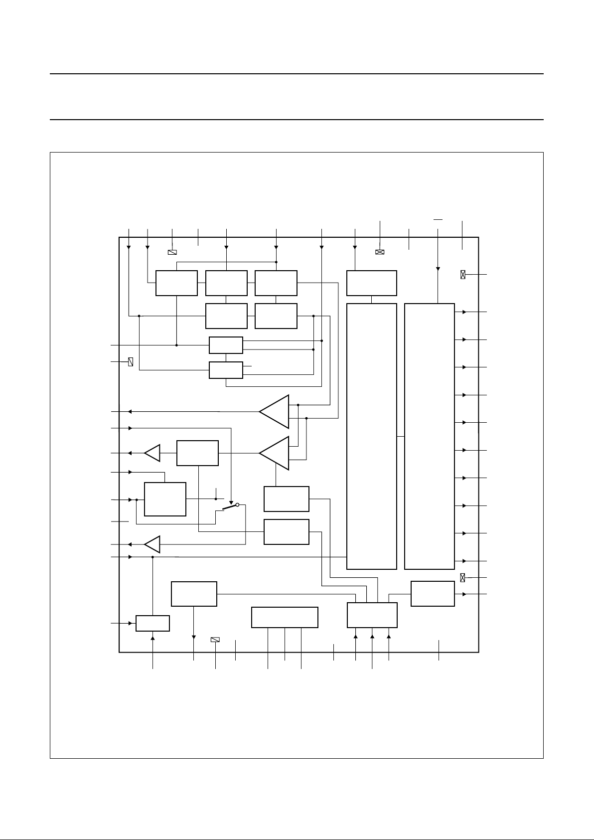
BLOCK DIAGRAM
Fig.1 Block diagram.
handbook, full pagewidth
MGE361
SOFT
CLIPPER
OPTICAL
BLACK
CLAMP
TRACK-
AND-HOLD
TRACK-
AND-HOLD
TRACK-
AND-HOLD
TRACK-
AND-HOLD
TRACK-
AND-HOLD
CLAMP
ref2
ref1
CLAMP
CLAMP
8-BIT DAC
4-BIT DAC
10-BIT DAC
9-BIT DAC
+
6 dB
AGC
CLOCK
GENERATOR
10-BIT ADC
REGULATOR
SERIAL
INTERFACE
OUTPUTS
BUFFER
5
4
1
1
2
7
8
6
9
10
14
11
12
13 15 16 17 18
20
21
22
23
24
36
3
25
26
27
28
29
30
31
32
33
34
35
3738394041424344
454846
47
IN2
IN1 AGND3
V
CCA3
CDSP2 CDSP1 CLPCDS CLK
DGND2
V
CCD2
OE
V
CCO
D9
D8
D7
D6
D5
D4
D3
D2
D1
D0
DGND1
OFDOUT
OGND
V
CCD1
STDBY
SEN
SCLK
SDATA
DEC1
V
RT
V
RB
V
CCA2
DACOUT
V
ref
CLPADC
AGND2
ADCIN
PBOUT
V
CCA1
PBIN
AGCOUT
PBK
CLPOPB
AGND1
19
STGE
AMPOUT
TDA8786
TDA8786A
1
Page 4

1997 Nov 17 4
Philips Semiconductors Product specification
10-bit analog-to-digital interface for
CCD cameras
TDA8786; TDA8786A
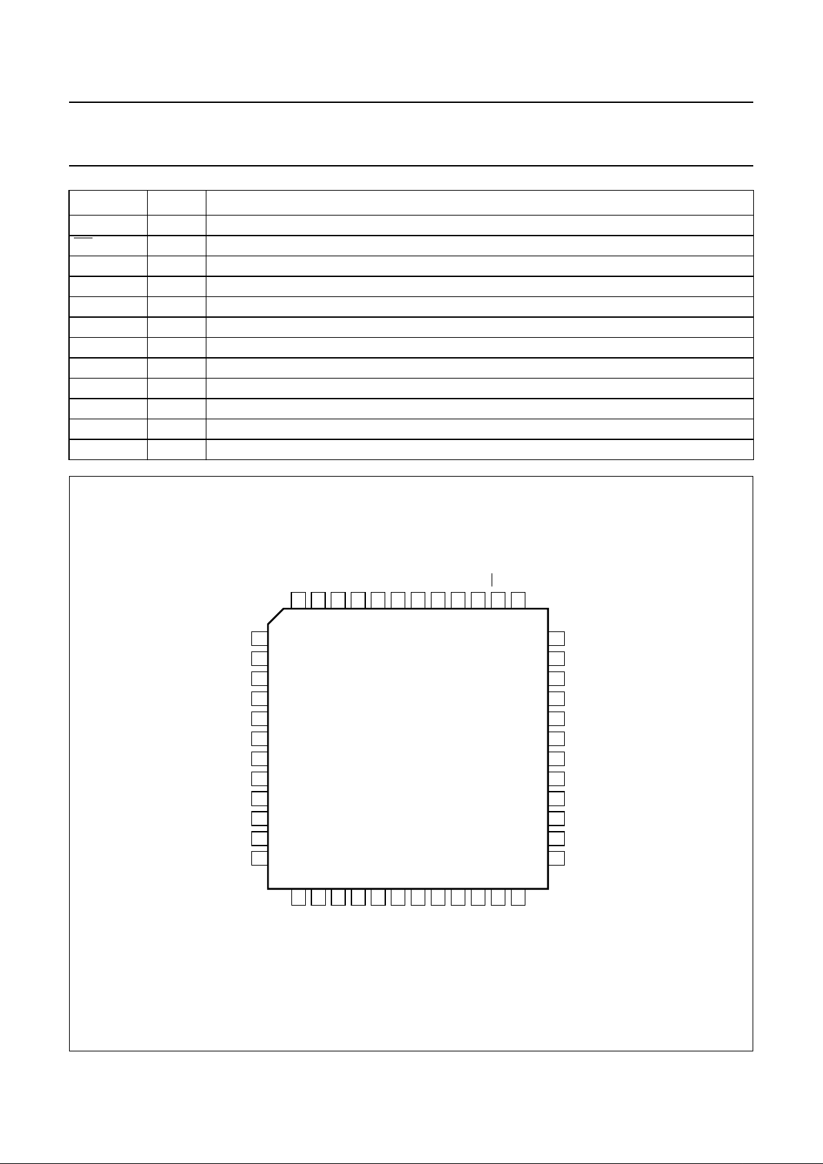
PINNING
SYMBOL PIN DESCRIPTION
CLPOPB 1 optical black clamp control pulse input (active HIGH for TDA8786, active LOW for TDA8786A)
PBK 2 pre-blanking control pulse input; if PBK is HIGH (LOW) the signal is replaced by the optical
black level for TDA8786 (TDA8786A)
OFDOUT 3 analog output of the additional 8-bit control DAC (controlled via the serial interface)
AMPOUT 4 CDS amplifier output (fixed gain = +6 dB)
AGND1 5 analog ground 1
V
CCA1
6 analog supply voltage 1
AGCOUT 7 AGC and soft clipper amplifier signal output
PBIN 8 optical black clamp and pre-blanking block signal input (from AGCOUT via a capacitor)
PBOUT 9 optical black clamp and pre-blanking block signal output
ADCIN 10 ADC analog signal input (from PBOUT or AGCOUT via a capacitor)
CLPADC 11 clamp control input for ADC analog input signal clamp (active HIGH for TDA8786 and active
LOW for TDA8786A)
V
ref
12 ADC input clamp reference voltage (normally connected to pin VRB or DACOUT)
DACOUT 13 DAC output for ADC clamp level
AGND2 14 analog ground 2
V
CCA2
15 analog supply voltage 2
V
RB
16 ADC reference voltage (BOTTOM) code 0
V
RT
17 ADC reference voltage (TOP) code 1023
DEC1 18 decoupling 1 (decoupled to ground via a capacitor)
STGE 19 CDS offset storage
SDATA 20 serial data input for the 4 control DACs (9-bit DAC for AGC gain, 4-bit DAC for soft clipper;
additional 8-bit DAC for OFD output voltage; 10-bit DAC for ADC clamp level and the stand-by
mode per block; see Table 1)
SCLK 21 serial clock input for the control DACs and their serial interface; see Table 1
SEN 22 enable input for the serial interface shift register (active when SEN = logic 0); see Table 1
STDBY 23 stand-by control pin (active HIGH); all the output bits are logic 0 when stand-by is enabled
V
CCD1
24 digital supply voltage 1
DGND1 25 digital ground1
D0 26 ADC digital output 0 (LSB)
D1 27 ADC digital output 1
D2 28 ADC digital output 2
D3 29 ADC digital output 3
D4 30 ADC digital output 4
D5 31 ADC digital output 5
D6 32 ADC digital output 6
D7 33 ADC digital output 7
D8 34 ADC digital output 8
D9 35 ADC digital output 9 (MSB)
OGND 36 digital output ground
Page 5
1997 Nov 17 5
Philips Semiconductors Product specification
10-bit analog-to-digital interface for
CCD cameras
TDA8786; TDA8786A
V
CCO
37 digital output supply voltage
OE 38 output enable (LOW: digital outputs active; HIGH: digital outputs high impedance)
V
CCD2
39 digital supply voltage 2
DGND2 40 digital ground2
CLK 41 ADC clock input
CLPCDS 42 CDS clamp control input (active HIGH for TDA8786; active LOW for TDA8786A)
CDSP1 43 CDS control pulse input 1 (active HIGH for TDA8786; active LOW for TDA8786A)
CDSP2 44 CDS control pulse input 2 (active HIGH for TDA8786; active LOW for TDA8786A)
V
CCA3
45 analog supply voltage 3
IN1 46 input signal 1 from CCD (usually black channel)
IN2 47 input signal 2 from CCD (usually video channel)
AGND3 48 analog ground 3
SYMBOL PIN DESCRIPTION
Fig.2 Pin configuration.
1
2
3
4
5
6
7
8
9
10
11
36
35
34
33
32
31
30
29
28
27
26
13
14
15
16
17
18
19
20
21
22
23
48
47
46
45
44
43
42
41
40
39
38
12
24 37
25
TDA8786
TDA8786A
MGE360
OGND
D9
D8
D7
D5
D4
D3
D2
D1
D0
DGND1
CLPOPB
PBK
OFDOUT
AMPOUT
AGND1
V
CCA1
PBIN
PBOUT
CLPADC
V
ref
D6
IN2
IN1
V
CCA3
CDSP2
CDSP1
CLPCDS
DGND2
V
CCD2
OE
V
CCO
AGND3
CLK
AGCOUT
ADCIN
AGND2
V
CCA2
V
RB
V
RT
DEC1
STGE
SDATA
SEN
STDBY
V
CCD1
DACOUT
SCLK
Page 6
1997 Nov 17 6
Philips Semiconductors Product specification
10-bit analog-to-digital interface for
CCD cameras
TDA8786; TDA8786A
LIMITING VALUES
In accordance with the Absolute Maximum Rating System (IEC 134).
Note
1. The supply voltages V
CCA
, V
CCD
and V
CCO
may have any value between −0.3 and +7.0 V provided that the supply
voltage difference ∆VCC remains as indicated.
HANDLING
Inputs and outputs are protected against electrostatic discharges in normal handling. However, to be totally safe, it is
desirable to take normal precautions appropriate to handling integrated circuits.
THERMAL CHARACTERISTICS
SYMBOL PARAMETER CONDITIONS MIN. MAX. UNIT
V
CCA
analog supply voltage note 1 −0.3 +7.0 V
V
CCD
digital supply voltage note 1 −0.3 +7.0 V
V
CCO
output stages supply voltage note 1 −0.3 +7.0 V
∆V
CC
supply voltage difference
between V
CCA
and V
CCD
−1.0 +1.0 V
between V
CCA
and V
CCO
−1.0 +4.0 V
between V
CCD
and V
CCO
−1.0 +4.0 V
V
i
input voltage referenced to V
SSA
−0.3 +7.0 V
V
CLK(p-p)
AC input voltage for switching
(peak-to peak-value)
referenced to V
SSD
− V
CCD
V
I
o
output current − 10 mA
T
stg
storage temperature −55 +150 °C
T
amb
operating ambient temperature −20 +75 °C
T
j
junction temperature − 150 °C
SYMBOL PARAMETER CONDITIONS VALUE UNIT
R
th(j-a)
thermal resistance from junction to ambient in free air 76 K/W
Page 7
1997 Nov 17 7
Philips Semiconductors Product specification
10-bit analog-to-digital interface for
CCD cameras
TDA8786; TDA8786A
CHARACTERISTICS
V
CCA=VCCD
= 4.75 V; V
CCO
= 2.6 V; f
CLK
= 18 MHz; T
amb
=25°C; unless otherwise specified.
SYMBOL PARAMETER CONDITIONS MIN. TYP. MAX. UNIT
Supplies
V
CCA
analog supply voltage 4.5 4.75 5.5 V
V
CCD
digital supply voltage 4.5 4.75 5.5 V
V
CCO
digital outputs supply
voltage
2.5 2.6 5.5 V
I
CCA
analog supply current − 83 − mA
I
CCD
digital supply current − 16 − mA
I
CCO
digital outputs supply
current
CL= 20 pF on all data
outputs; ramp input
− 1 − mA
Digital inputs
C
LOCK INPUT: CLK (REFERENCED TO DGND)
V
IL
LOW-level input voltage 0 − 0.8 V
V
IH
HIGH-level input voltage 2.0 − V
CCD
V
I
IL
LOW-level input current V
CLK
= 0.8 V −1 − +1 µA
I
IH
HIGH-level input current V
CLK
= 2.0 V −−20 µA
Z
i
input impedance f
CLK
= 18 MHz − 2 − kΩ
C
i
input capacitance f
CLK
= 18 MHz − 2 − pF
INPUTS: CDSP1 AND CDSP2
V
IL
LOW-level input voltage 0 − 0.6 V
V
IH
HIGH-level input voltage 2.2 − V
CCD
V
I
IL
LOW-level input current VIL= 0.6 V −−100 −µA
I
IH
HIGH-level input current VIH= 2.2 V − 0 −µA
INPUTS: SEN, STDBY, CLPCDS, CLPOPB, PBK AND CLPADC
V
IL
LOW-level input voltage 0 − 0.6 V
V
IH
HIGH-level input voltage 2.2 − V
CCD
V
I
i
input current −2 − +2 µA
INPUTS: SEN, SDATA AND SCLK (see Fig.14)
t
su1
SEN set-up time compared
to SCLK rising edge
− 4 − ns
t
su2
SDATA set-up time
compared to SCLK rising
edge
− 4 − ns
t
su3
SEN set-up time compared
to SCLK falling edge
− 4 − ns
t
hd3
SEN hold time compared
to SCLK rising edge
− 4 − ns
t
hd4
SDATA hold time
compared to SCLK rising
edge
− 4 − ns
Page 8
1997 Nov 17 8
Philips Semiconductors Product specification
10-bit analog-to-digital interface for
CCD cameras
TDA8786; TDA8786A
Correlated Double Sampling; CDS
V
i(CDS)(p-p)
CDS input amplitude
(peak-to-peak value)
− 400 1200 mV
I
STGE,IN1,IN2
input current pins 19, 46
and 47
−2 − +2 µA
t
CDS(min)
CDS control pulses
minimum active time
(HIGH for TDA8786,
LOW for TDA8786A)
f
i(CDS1,2)=fCLK(pix)
V
i(CDS)(p-p)
= 1200 mV
black-to-white transition in
one pixel (±1 LSB typ.)
12 −−ns
t
hd1
hold time IN1 compared to
control pulse CDSP1
see Fig.15 − 1 − ns
t
hd2
hold time of IN2 compared
to control pulse CDSP2
see Fig.15 −−0.5 − ns
Amplifier outputs
G
AMPOUT
output amplifier gain − 6 − dB
Z
AMPOUT
output amplifier
impedance
− 300 −Ω
V
AMPOUT(p-p)
output amplifier dynamic
voltage level
(peak-to-peak value)
− 2.4 − V
V
AMPOUT(bl)
output amplifier black
level voltage
− 1.1 − V
V
AGCOUT(p-p)
AGC output amplifier
dynamic voltage level
(peak-to-peak value)
− 1800 − mV
V
AGCOUT
AGC output amplifier black
level voltage
− 1.1 − V
Z
AGCOUT
AGC output amplifier
output impedance
at 10 kHz − 5 −Ω
I
AGCOUT
AGC output static drive
current
static −−1mA
V
OPB(p-p)
optical black clamp and
blanking block output
dynamic voltage
(peak-to-peak value)
− 1.8 − V
V
OPB
optical black clamp and
blanking block output black
level voltage
− 1.4 − V
Z
OPB
optical black clamp and
blanking block output
impedance
at 10 kHz −−5Ω
I
OPB
OPB output current drive static −−1mA
I
PBIN
input current pin 8 −2 − +2 µA
G
AGC(min)
minimum gain of AGC
circuit
AGC DAC input code = 00
(9-bit control)
− 3.5 − dB
SYMBOL PARAMETER CONDITIONS MIN. TYP. MAX. UNIT
Page 9
1997 Nov 17 9
Philips Semiconductors Product specification
10-bit analog-to-digital interface for
CCD cameras
TDA8786; TDA8786A
G
AGC(max)
maximum gain of AGC
circuit
AGC DAC input
code = ≥319 (9-bit control)
− 33.5 − dB
V
AGCOUT
AGC output amplifier black
level voltage
− 1.1 − V
V
inflex(p-p)
voltage at soft clipper
inflexion point
(peak-to-peak value)
soft clipper 4-bit control
DAC input code = 00
− 40%
V
AGCOUT(p-p)
− V
soft clipper 4-bit control
DAC input code = 15
− 100%
V
AGCOUT(p-p)
− V
CR
sc
soft clipper compression
ratio
V
i(sc)<Vinflex
− 1.0 −
V
i(sc)>Vinflex
− 0.66 −
CLAMPS
g
mADC
ADC clamps
transconductance
at clamp level − 60 − mS
g
mPBK
PBK clamp
transconductance
at clamp level − 60 − mS
g
mCDS
CDS clamps
transconductance
at clamp level − 5.5 − mS
V
PBIN(clamp)
clamp voltage
at PBIN input
− 1.4 − V
Analog-to-Digital Converter; ADC
f
CLK(max)
maximum clock frequency 18 −−MHz
t
CPH
clock pulse width HIGH 15 −−ns
t
CPL
clock pulse width LOW 15 −−ns
SR
CLK
clock input slew rate
(rising and falling edge)
10 to 90% 0.5 −−V/ns
V
i(ADC)(p-p)
ADC input voltage level
(peak-to-peak value)
− 1.8 − V
V
RB
ADC reference voltage
output code 0
− 1.4 − V
V
RT
ADC reference voltage
output code 1023
− 3.2 − V
I
ADCIN
input current pin 10 −2 − +2 µA
ILE integral linearity error f
CLK
= 18 MHz; ramp input −±1.0 ±2.0 LSB
DLE differential linearity error f
CLK
= 18 MHz; ramp input −±0.4 ±0.75 LSB
t
d(s)
sampling delay time −−5ns
SYMBOL PARAMETER CONDITIONS MIN. TYP. MAX. UNIT
Page 10

1997 Nov 17 10
Philips Semiconductors Product specification
10-bit analog-to-digital interface for
CCD cameras
TDA8786; TDA8786A
Total chain timing (CDS + ADC + SOFT CLIPPER + PRE BLANKING + ADC)
t
d
time delay between
CDSP1 and CLK
50% at rising edges of
CLK and CDSP1:
transition full-scale code 0
to code 1023;
V
i(CDS)(p-p)
= 1200 mV
− 40 − ns
N
(rms)
noise (RMS value) gain = 3.5 dB − 0.5 − LSB
Digital-to-Analog Converters (OFDOUT DAC)
V
OFDOUT(p-p)
additional 8-bit control
DAC (OFD) output voltage
(peak-to-peak value)
− 1.4 − V
V
OFDOUT(0)
DC output voltage for
code 0
− 2.0 − V
V
OFDOUT(255)
DC output voltage for
code 255
− 3.4 − V
Z
OFDOUT
additional 8-bit control
DAC (OFD) output
impedance
− 2000 −Ω
I
OFDOUT
OFD output current drive static −−50 µA
ADC clamp control DAC (see Fig.5)
V
DACOUT(p-p)
ADC clamp 10-bit control
DAC output voltage
(peak-to-peak value)
− 0.9 − V
V
DACOUT
DC output voltage code 0 − 1.4 − V
code 1023 − 2.3 − V
Z
DACOUT
ADC clamp control DAC
output impedance
−−250 Ω
I
DACOUT
DAC output current drive static −−50 µA
OFE
LOOP
maximum offset error of
DAC + ADC clamp loop
code 0 −± 5 − LSB
code 1023 −±5−LSB
SYMBOL PARAMETER CONDITIONS MIN. TYP. MAX. UNIT
Page 11

1997 Nov 17 11
Philips Semiconductors Product specification
10-bit analog-to-digital interface for
CCD cameras
TDA8786; TDA8786A
Digital outputs (f
CLK
= 18 MHz; CL=20pF)
V
OH
HIGH-level output voltage IOH= −1mA V
CCO
− 0.5 − V
CCO
V
V
OL
LOW-level output voltage IOL= 1 mA 0 − 0.5 V
I
OZ
output current in 3-state
mode
0.5 V < Vo< V
CCO
−20 − +20 µA
t
o(h)
output hold time 5 −−ns
t
o(d)
output delay Ci= 20 pF; V
CCO
= 4.75 V − 12 15 ns
C
i
= 20 pF; V
CCO
= 3.15 V − 17 20 ns
C
i
= 20 pF; V
CCO
= 2.7 V − 21 24 ns
Serial interface
f
SCLK(max)
maximum frequency of
serial interface
5 −−MHz
SYMBOL PARAMETER CONDITIONS MIN. TYP. MAX. UNIT
Fig.3 AGC gain as a function of DAC input code.
handbook, halfpage
MGE365
G
AGC
(dB)
33.5
3.5
0 319
511
AGC control DAC input code
Page 12

1997 Nov 17 12
Philips Semiconductors Product specification
10-bit analog-to-digital interface for
CCD cameras
TDA8786; TDA8786A
handbook, full pagewidth
MGE364
AGCOUT
100%
40%
40%
control DAC
input code = 15
control DAC
input code = 00
100% 130%
soft clipper input
0
(1)
(2)
0
Fig.4 Soft clipper output voltage as a function of soft clipper input voltage.
(1)
(2)
V
o
V
i
------
1=
V
o
V
i
------
0.66=
Fig.5 DAC voltage output as a function of DAC input code.
handbook, halfpage
MGE366
0
ADC CLAMP DAC
voltage
output
(V)
2.3
1.4
1023
ADC CLAMP control DAC input code
handbook, halfpage
MGD599
0
OFD DAC
voltage
output
(V)
3.4
2.0
255
OFD control DAC input code
Page 13

1997 Nov 17 13
Philips Semiconductors Product specification
10-bit analog-to-digital interface for
CCD cameras
TDA8786; TDA8786A
Fig.6 CCD high band control signal timing (TDA8786).
handbook, full pagewidth
MGE370
>12 ns
>12 ns
CDSP1
CDSP2
8 × f
SC
= 2f
CLK
Fig.7 CCD normal band control signal timing (TDA8786).
handbook, full pagewidth
MGE369
>12 ns
>12 ns
CDSP1
CDSP2
8 × f
SC
= 3f
CLK
Page 14

1997 Nov 17 14
Philips Semiconductors Product specification
10-bit analog-to-digital interface for
CCD cameras
TDA8786; TDA8786A
Fig.8 CCD high band control signal timing (TDA8786A).
handbook, full pagewidth
MGE371
>12 ns
>12 ns
CDSP1
CDSP2
8 × f
SC
= 2f
CLK
Fig.9 CCD normal band control signal timing (TDA8786A).
handbook, full pagewidth
MGE372
8 × f
SC
= 3f
CLK
CDSP1
CDSP2
>12 ns
>12 ns
Page 15

1997 Nov 17 15
Philips Semiconductors Product specification
10-bit analog-to-digital interface for
CCD cameras
TDA8786; TDA8786A
Fig.10 Typical PBK clamp current.
handbook, halfpage
MBK058
450
0
−450
I
PBIN
(µA)
V
PBIN
(V)
30 mV
1.4
Fig.11 Typical clamp currents for pins IN1, IN2 and
STGE.
handbook, halfpage
MBK057
350
0
−350
I
(µA)
V (V)
200 mV
2.85
Fig.12 Typical ADC clamp current.
handbook, halfpage
MBK059
450
slope = 1 kΩ
0
−450
I
ADCIN
(µA)
V
ADCIN
(V)
500 mV
30 mV
V
ref
ADC clamping
When pin CLPADC is HIGH (TDA8786) (LOW for
TDA8786A), the ADC input is clamped to voltage level V
ref
.
V
ref
should normally be connected to VRB (ADC reference
voltage code 0) or to DACOUT (10-bit DAC output).
The DAC is controlled via the serial interface, its output
covers the lower half of the ADC input range.
Page 16

1997 Nov 17 16
Philips Semiconductors Product specification
10-bit analog-to-digital interface for
CCD cameras
TDA8786; TDA8786A
Fig.13 Serial interface block diagram.
handbook, full pagewidth
OFD
LATCHES
AGC GAIN
LATCHES
SOFT CLIP
LATCHES
PARTIAL
STANDBY
CLAMP
REFERENCE
LATCHES
LATCH
SELECTION
D0
LSB MSB
SDATA
SCLK
SEN
8-bit DAC 10-bit DAC
MGD526
AGC control soft clip
control
standby
control
D1 D2 D3 D4 D510D6
SHIFT REGISTER
D7 D8 D9 A0 A1 A2
8
(D7 to D0)
9
(D8 to D0)
4
(D3 to D0)
4
(D3 to D0)
10
(D9 to D0)
Fig.14 Loading sequence of control DACs input data via the serial interface.
tsu= 4ns (min.); t
hd3=thd4
= 4ns (min.).
handbook, full pagewidth
MGE373
A2SDATA
SCLK
SEN
A1 A0 D9 D7 D6 D5 D4 D3
MSB LSB
D2 D1 D0
t
hd3
t
su3
t
su1
t
hd4
t
su2
D8
Page 17

1997 Nov 17 17
Philips Semiconductors Product specification
10-bit analog-to-digital interface for
CCD cameras
TDA8786; TDA8786A
Table 1 Serial interface programming (see note 1)
Note
1. At the end of each programming sequence (usually during the video vertical blanking), the soft clipper register must
be reloaded (for example if the soft clipper is not used, code 15 must be entered in the soft clipper register at the end
of each TDA8786(A) programming sequence).
Table 2 Standby selection
ADDRESS BITS
DATA BITS D9 to D0
A2 A1 A0
0 0 0 OFDOUT output control (D7 to D0).
0 0 1 Soft clipper control. Only the 4 LSBs (D3 to D0) are used. Bits D9 to D4 should be set to
logic 0.
0 1 0 AGC gain control (D8 to D0).
0 1 1 Partial standby controls for power consumption optimization. Only the 4 LSBs (D3 to D0)
are used. Bits D9 to D4 should be set to logic 0:
D0 = 1: CDS + AGC + soft clipper block in standby; I
CCA+ICCD
=48mA
D1 = 1: optical black clamp + blanking block in standby; I
CCA+ICCD
=92mA
D2 = 1: OFD DAC in standby; I
CCA+ICCD
=98mA
D3 = 1: 6 dB amplifier (output on AMPOUT pin) in standby; I
CCA+ICCD
= 98.5 mA.
1 0 0 Clamp reference DAC (D9 to D0).
STDBY D9 to D0 I
CCA+ICCD
1 LOW 4 mA (typ.)
0 active 99 mA (typ.)
Page 18

1997 Nov 17 18
Philips Semiconductors Product specification
10-bit analog-to-digital interface for
CCD cameras
TDA8786; TDA8786A
Fig.15 Pixel frequency timing diagram.
The hatched areas represent active video.
handbook, full pagewidth
MGE367
IN1 and IN2
CDSP1
(active HIGH)
CDSP2
(active HIGH)
DATA
OUTPUT
D0 to D7
CLK
PIXEL N − 4 PIXEL N − 3 PIXEL N − 2 PIXEL N − 1
PIXEL
N
PIXEL
N + 1
PIXEL
N + 2
PIXEL
N + 3
PIXEL
N + 4
PIXEL N
t
d (OUT)
sample N
t
h
t
d
t
hd2
t
hd1
Fig.16 Line frequency timing diagram.
handbook, full pagewidth
MGE368
CLPCDS
(active HIGH)
CLPADC
(active HIGH)
CLPOPB
(active HIGH)
PBK
(active HIGH)
PREBLANKING
OUTPUT
AGCOUT VIDEO OPTICAL BLACK HORIZONTAL FLYBACK DUMMY VIDEO
VIDEO BLACK LEVEL VIDEO
Page 19

1997 Nov 17 19
Philips Semiconductors Product specification
10-bit analog-to-digital interface for
CCD cameras
TDA8786; TDA8786A
APPLICATION INFORMATION
TDA8786 and SAA8110 can be used with Sharp CCDs. TDA8786A and SAA8110 can be used with Sony CCDs. Table 3
gives as an example some references of ICs which may be used with Philips TDA8786(A)/SAA8110. This overview is
not restrictive, both devices are compatible with other CCD/V-driver/PPG combinations including the more recent ones.
Table 3 Possible components for the application of Figs 17 and 18
Notes to the application diagram
1. In the configuration of Figs 17 and 18, the microcontroller reads and writes data from/to the DSP using the
SNERT-bus (UART mode 0). Optional external control is available via the I2C-bus.
2. Free I/O pins of the microcontroller can be used to control PGG, or for other purposes.
3. 83Cxxx processing is synchronized by VD interruption. Depending on VD polarity, it can be necessary to invert VD.
4. A customized 83Cxxx is available for this application. Please contact your nearest Philips sales office.
CCD TYPE
COMPONENT
TYPE
NTSC PAL
MEDIUM
RESOLUTION
HIGH
RESOLUTION
MEDIUM
RESOLUTION
HIGH
RESOLUTION
Sony CCDs CCD LZ2313H5 LZ2353A LZ2323H5 LZ2363
V-driver LR36683N
timing generator LZ95G55 LZ95G71 LZ95G55 LZ95G71
Sharp CCDs CCD ICX056AK ICX068AK ICX057AK ICXo69AK
V-driver CXD1250MN, CXD1267N
timing generator CXD1257AR CXD1265R CXD1257AR CXD1265R
Page 20

1997 Nov 17 20
Philips Semiconductors Product specification
10-bit analog-to-digital interface for
CCD cameras
TDA8786; TDA8786A
Fig.17 SAA8110G system configuration for camera application (continued in Fig.18).
handbook, full pagewidth
P0 (optional, PPG setting)
P1 (optional, PPG settings)
CDAC
OUT
(optional, can be used for frequency tuning)
CLK1 (to ADC and DSP)
CLK2 (to DSP, CLK2 = 2 × CLK1)
CDSPULSE1
CDSPULSE2
CLAMPCDS (CLAMP CDS, OPB, ADC can be the same)
CLAMPOPB
CLAMPADC
PreBlank (optional)
HD (to DSP and µC)
VD (to DSP and µC)
FI (to DSP and µC)
P0
P1
CDAC
OUT
CLK1
CLK2
CDSPULSE1
CDSPULSE2
CLAMPCDS
CLAMPOPB
CLAMPADC
PreBlank
Horizontal Drive
Vertical Drive
Field Id
V4 V3 V2 V1 H1
VERTICAL DRIVER
(PPG)
H2
V4 V3 V2 V1 H1 H2
Electrical
Shutter
Reset
Pulse
OGND
D9
D8
D7
D6
D5
D4
D3
D2
D1
D0
100
nF
1 nF
1nF1nF2.2
nF
200
nF
DGND1
36
35
34
33
32
31
30
29
28
27
26
25
CLPOPB
CLK1
100 nF
100 nF
100 nF
100 nF
100 nF
OEN (optional)
(from microcontroller)
100 nF
V
DDD
V
DDD
CLAMPCDS
CDSPULSE1
CDSPULSE2
PBK
CLAMPOPB
PreBlank
OFDOUT
AMPOUT
AMPOUT
AGND1
V
CCA1
AGCOUT
PBIN
PBOUT
ADCIN
CLPADC
V
ref
1
2
3
4
5
6
7
8
9
10
11
12
TDA8786G
or
TDA8786AG
ANALOG-TO-DIGITAL INTERFACE
AGND3
IN2
IN1
V
CCA3
V
CCD2
CDSP2
CDSP1
CLPCDS
DGND2
V
CCO
OE
CLK
DACOUT
AGND2
V
CCA2
V
RB
SEN
V
RT
DEC1
STGE
SCLK
V
CCD1
STBY
SDATA
13 14 15 16 2217 18 19 21 242320
48 47
220 nF
220 nF
CLAMPADC
(from PPG)
46 45 3944 43 42 40 373841
VERTICAL
DRIVER BUFFER
CCD
SMP_CLK
(from DSP)
V
DDD
V
DDA1
V
DDA1
V
DDA1
V
DDA1
−xxV +xxV
SWITCH MODE
POWER SUPPLIES
(optional)
CCDout
OFD level
(optional)
1 µF
A
B
C
D
E
F
G
H
I
J
K
L
M
5
6
7
8
2
VD (from PPG)
3
4
5
10 µF
4
3
2
1
SDA
SCL
PTC
V
DD
A2
100 nF
NC
WP
V
SS
6
7
8
9
4.7 µF
12 MHz
A0/SN
DA
SCL/SN
CL
HD (opt.)
FI
IN
A1/SN
RES
10
11
83C54/
83C654
(OM-XXX)
MICRO-
CONTROLLER
EPROM
PCF8598
PCF8594
PCF8582
13
14
15
16
17
18
19
20
21
22
18 pF
18 pF
V
DD
V
DDD
V
DDD
V
DDD
V
DDD
V
DDD
V
DDD
V
DDD
P0.0/AD0
P0.1/AD1
P0.2/AD2
P0.3/AD3
P0.4/AD4
P0.5/AD5
RESET_DSP
(to DSP)
P0.6/AD6
P0.7/AD7
EA
ALE
PSEN
P2.7/A15
P2.6/A14
P2.5/A13
P2.4/A12
P2.3/A11
P2.2/A10
P2.1/A9
P2.0/A8
44
43
42
41
OEN (optional)
(to ADC)
BC848C
40
39
38
37
36
35
33
32
31
30
29
28
27
26
25
24
P1.0
P1.1
P1.2
P1.3
P1.4
P1.5
P1.6/SCL
P1.7/SDA
RST
P3.0/RxD
P3.1/TxD
P3.2/INT0
P3.3/INT1
P3.4/T0
P3.5/T1
P3.6/WR
P3.7/RD
XTAL2
XTAL1
V
SS
5 V V
DDA1
5 V V
DDA2
5 V V
DDA3
V
DDD
4JB
3JB
2JB
1
+5 V
GND
SCL
SDA JB
10 kΩ
4.7kΩ4.7
kΩ
10 kΩ
MGK393
digital ground
analog ground
Shutter
Reset
Page 21

1997 Nov 17 21
Philips Semiconductors Product specification
10-bit analog-to-digital interface for
CCD cameras
TDA8786; TDA8786A
Fig.18 SAA8110G system configuration for camera application (continued from Fig.17).
(1) Values depend on DSP output configuration.
handbook, full pagewidth
MGK394
1
3
5
7
9
11
13
15
17
19
2
4
6
8
10
SAA8110G
DIGITAL SIGNAL PROCESSOR
12
14
16
18
20
10 nF
100 nF
100
nF
100 nF
100 nF
100 nF
SMP_CLK (to power supply)
P0
digital ground
analog ground
P1
RESET_DSP
(from µC)
21
V
DDA2
V
DDA3
V
DDA3
V
DDA3
V
DDA3
22 23 24 25 26 27 28 29 30 31 32 33 34 35 36 37
68 Ω
68 Ω
68 Ω
47 kΩ
150 kΩ
38 39 40
80 79
100 nF
A1/SN
RES
A0/SN
DA
SDA
optional
SCL/SN
CL
78 77 76 75 74 73 72 71 70 69 68 67 66 65 64 63 62 61
60
58
56
54
52
50
48
46
44
42
59
57
55
53
51
49
47
45
43
41
CVBS-RCA
CVBS
V, Red
U, Blue
C
Green
Y
SVHS
3
4
1
2
3
4
5
11
12
13
14
15
6
7
8
9
10
126
7
5
V
DDD(C1)
VSYNC
IN
VD
FI
IN
FI
CCD9
CCD7
CCD5
CCD3
CCD1
V
SSD(C2)
V
DDD
V
DDD
V
SSA(CD)
CLK1
CLK1
HSYNC
IN
HD
V
SSD(C1)
V
DDD
CCD8
CCD6
CCD4
CCD2
CCD0
SCLK
CDAC
RBIAS
V
DDA(CD)
SDATA
STROBE
SMP
P0
P1
SIS
V
DDD(C2)
RESET
T2T1T0
V
SSA(OB)
OUT3
V
DDA(O3)
OUT2
V
DDA(O2)
OUT1
V
DDA(O1)
CDAC
OUT
CDAC
OUT
UV1
100 nF
100
nF
UV7
LLC
HREF
FI
OUT
V
DDD(P1)
RBIAS
V
SSA(BG)
UV2
UV3
UV4
UV5
UV6
V
SSD(P1)
V
DDD(P2)
V
DDD
V
DDD
CREF/PXQ
VSYNC
OUT
CLK2
CLK2 (from PPG)
V
DDA(BG)
DECOUPL
100 nF
100 nF
100 nF
V
DDA(DC)
X
OUT
A0/SN
DA
V
DDD(C3)
Y0
Y2
Y4
Y6
X
IN
V
SSD(C4)
SCL/SN
CL
V
SSD(C3)
SDA
A1/SN
RES
V
SSD(P2)
Y1
Y3
Y5
Y7
UV0
V
DDD
V
DDD
V
DDD
26
24
22
20
18
16
DIGITAL OUTPUT CONNECTOR
14
12
10
8
6
4
2
25
23
21
19
17
15
13
11
9
7
5
3
1
L
(1)
L
(1)
L
(1)
L
(1)
L
(1)
L
(1)
L
(1)
L
(1)
L
(1)
A
B
C
D
E
F
G
H
I
J
K
L
M
Page 22

1997 Nov 17 22
Philips Semiconductors Product specification
10-bit analog-to-digital interface for
CCD cameras
TDA8786; TDA8786A
PACKAGE OUTLINE
UNIT
A
max.
A1A2A3b
p
cE
(1)
eH
E
LL
p
Zywv θ
REFERENCES
OUTLINE
VERSION
EUROPEAN
PROJECTION
ISSUE DATE
IEC JEDEC EIAJ
mm
1.60
0.20
0.05
1.45
1.35
0.25
0.27
0.17
0.18
0.12
7.1
6.9
0.5
9.15
8.85
0.95
0.55
7
0
o
o
0.12 0.10.21.0
DIMENSIONS (mm are the original dimensions)
Note
1. Plastic or metal protrusions of 0.25 mm maximum per side are not included.
0.75
0.45
SOT313-2
94-12-19
97-08-01
D
(1) (1)(1)
7.1
6.9
H
D
9.15
8.85
E
Z
0.95
0.55
D
b
p
e
E
B
12
D
H
b
p
E
H
v M
B
D
Z
D
A
Z
E
e
v M
A
1
48
37
36
25
24
13
θ
A
1
A
L
p
detail X
L
(A )
3
A
2
X
y
c
w M
w M
0 2.5 5 mm
scale
pin 1 index
LQFP48: plastic low profile quad flat package; 48 leads; body 7 x 7 x 1.4 mm
SOT313-2
Page 23

1997 Nov 17 23
Philips Semiconductors Product specification
10-bit analog-to-digital interface for
CCD cameras
TDA8786; TDA8786A
SOLDERING
Introduction
There is no soldering method that is ideal for all IC
packages. Wave soldering is often preferred when
through-hole and surface mounted components are mixed
on one printed-circuit board. However, wave soldering is
not always suitable for surface mounted ICs, or for
printed-circuits with high population densities. In these
situations reflow soldering is often used.
This text gives a very brief insight to a complex technology.
A more in-depth account of soldering ICs can be found in
our
“IC Package Databook”
(order code 9398 652 90011).
Reflow soldering
Reflow soldering techniques are suitable for all LQFP
packages.
Reflow soldering requires solder paste (a suspension of
fine solder particles, flux and binding agent) to be applied
to the printed-circuit board by screen printing, stencilling or
pressure-syringe dispensing before package placement.
Several methods exist for reflowing; for example,
infrared/convection heating in a conveyor type oven.
Throughput times (preheating, soldering and cooling) vary
between 50 and 300 seconds depending on heating
method. Typical reflow peak temperatures range from
215 to 250 °C.
Wave soldering
Wave soldering is not recommended for LQFP packages.
This is because of the likelihood of solder bridging due to
closely-spaced leads and the possibility of incomplete
solder penetration in multi-lead devices.
CAUTION
Wave soldering is NOT applicable for all LQFP
packages with a pitch (e) equal or less than 0.5 mm.
If wave soldering cannot be avoided, for LQFP
packages with a pitch (e) larger than 0.5 mm, the
following conditions must be observed:
• A double-wave (a turbulent wave with high upward
pressure followed by a smooth laminar wave)
soldering technique should be used.
• The footprint must be at an angle of 45° to the board
direction and must incorporate solder thieves
downstream and at the side corners.
During placement and before soldering, the package must
be fixed with a droplet of adhesive. The adhesive can be
applied by screen printing, pin transfer or syringe
dispensing. The package can be soldered after the
adhesive is cured.
Maximum permissible solder temperature is 260 °C, and
maximum duration of package immersion in solder is
10 seconds, if cooled to less than 150 °C within
6 seconds. Typical dwell time is 4 seconds at 250 °C.
A mildly-activated flux will eliminate the need for removal
of corrosive residues in most applications.
Repairing soldered joints
Fix the component by first soldering two diagonallyopposite end leads. Use only a low voltage soldering iron
(less than 24 V) applied to the flat part of the lead. Contact
time must be limited to 10 seconds at up to 300 °C. When
using a dedicated tool, all other leads can be soldered in
one operation within 2 to 5 seconds between
270 and 320 °C.
Page 24

1997 Nov 17 24
Philips Semiconductors Product specification
10-bit analog-to-digital interface for
CCD cameras
TDA8786; TDA8786A
DEFINITIONS
LIFE SUPPORT APPLICATIONS
These products are not designed for use in life support appliances, devices, or systems where malfunction of these
products can reasonably be expected to result in personal injury. Philips customers using or selling these products for
use in such applications do so at their own risk and agree to fully indemnify Philips for any damages resulting from such
improper use or sale.
Data sheet status
Objective specification This data sheet contains target or goal specifications for product development.
Preliminary specification This data sheet contains preliminary data; supplementary data may be published later.
Product specification This data sheet contains final product specifications.
Limiting values
Limiting values given are in accordance with the Absolute Maximum Rating System (IEC 134). Stress above one or
more of the limiting values may cause permanent damage to the device. These are stress ratings only and operation
of the device at these or at any other conditions above those given in the Characteristics sections of the specification
is not implied. Exposure to limiting values for extended periods may affect device reliability.
Application information
Where application information is given, it is advisory and does not form part of the specification.
Page 25

1997 Nov 17 25
Philips Semiconductors Product specification
10-bit analog-to-digital interface for
CCD cameras
TDA8786; TDA8786A
NOTES
Page 26

1997 Nov 17 26
Philips Semiconductors Product specification
10-bit analog-to-digital interface for
CCD cameras
TDA8786; TDA8786A
NOTES
Page 27

1997 Nov 17 27
Philips Semiconductors Product specification
10-bit analog-to-digital interface for
CCD cameras
TDA8786; TDA8786A
NOTES
Page 28

Internet: http://www.semiconductors.philips.com
Philips Semiconductors – a worldwide company
© Philips Electronics N.V. 1997 SCA56
All rights are reserved. Reproduction in whole or in part is prohibited without the prior written consent of the copyright owner.
The information presented in this document does not form part of any quotation or contract, is believed to be accurate and reliable and may be changed
without notice. No liability will be accepted by the publisher for any consequence of its use. Publication thereof does not convey nor imply any license
under patent- or other industrial or intellectual property rights.
Netherlands: Postbus 90050, 5600PB EINDHOVEN, Bldg. VB,
Tel. +31 40 27 82785, Fax. +31 40 27 88399
New Zealand: 2 Wagener Place, C.P.O. Box 1041, AUCKLAND,
Tel. +64 9 849 4160, Fax. +64 9 849 7811
Norway: Box 1, Manglerud 0612, OSLO,
Tel. +47 22 74 8000, Fax. +47 22 74 8341
Philippines: Philips Semiconductors Philippines Inc.,
106 Valero St. Salcedo Village, P.O. Box 2108 MCC, MAKATI,
Metro MANILA, Tel. +63 2 816 6380, Fax. +63 2 817 3474
Poland: Ul. Lukiska 10, PL 04-123 WARSZAWA,
Tel. +48 22 612 2831, Fax. +48 22 612 2327
Portugal: see Spain
Romania: see Italy
Russia: Philips Russia, Ul. Usatcheva 35A, 119048 MOSCOW,
Tel. +7 095 755 6918, Fax. +7 095 755 6919
Singapore: Lorong 1, Toa Payoh, SINGAPORE 1231,
Tel. +65 350 2538, Fax. +65 251 6500
Slovakia: see Austria
Slovenia: see Italy
South Africa: S.A. PHILIPS Pty Ltd., 195-215 Main Road Martindale,
2092 JOHANNESBURG, P.O. Box 7430 Johannesburg 2000,
Tel. +27 11 470 5911, Fax. +27 11 470 5494
South America: Al. Vicente Pinzon, 173, 6th floor,
04547-130 SÃO PAULO, SP, Brazil,
Tel. +55 11 821 2333, Fax. +55 11 821 2382
Spain: Balmes 22, 08007 BARCELONA,
Tel. +34 3 301 6312, Fax. +34 3 301 4107
Sweden: Kottbygatan 7, Akalla, S-16485 STOCKHOLM,
Tel. +46 8 632 2000, Fax. +46 8 632 2745
Switzerland: Allmendstrasse 140, CH-8027 ZÜRICH,
Tel. +41 1 488 2686, Fax. +41 1 481 7730
Taiwan: Philips Semiconductors, 6F, No. 96, Chien Kuo N. Rd., Sec. 1,
TAIPEI, Taiwan Tel. +886 2 2134 2865, Fax. +886 2 2134 2874
Thailand: PHILIPS ELECTRONICS (THAILAND) Ltd.,
209/2 Sanpavuth-Bangna Road Prakanong, BANGKOK 10260,
Tel. +66 2 745 4090, Fax. +66 2 398 0793
Turkey: Talatpasa Cad. No. 5, 80640 GÜLTEPE/ISTANBUL,
Tel. +90 212 279 2770, Fax. +90 212 282 6707
Ukraine: PHILIPS UKRAINE, 4 Patrice Lumumba str., Building B, Floor 7,
252042 KIEV, Tel. +380 44 264 2776, Fax. +380 44 268 0461
United Kingdom: Philips Semiconductors Ltd., 276 Bath Road, Hayes,
MIDDLESEX UB3 5BX, Tel. +44 181 730 5000, Fax. +44 181 754 8421
United States: 811 East Arques Avenue, SUNNYVALE, CA 94088-3409,
Tel. +1 800 234 7381
Uruguay: see South America
Vietnam: see Singapore
Yugoslavia: PHILIPS, Trg N. Pasica 5/v, 11000 BEOGRAD,
Tel. +381 11 625 344, Fax.+381 11 635 777
For all other countries apply to: Philips Semiconductors,
International Marketing & Sales Communications, Building BE-p,
P.O. Box 218, 5600 MD EINDHOVEN, The Netherlands, Fax. +31 40 27 24825
Argentina: see South America
Australia: 34 Waterloo Road, NORTH RYDE, NSW 2113,
Tel. +61 2 9805 4455, Fax. +61 2 9805 4466
Austria: Computerstr. 6, A-1101 WIEN, P.O. Box 213, Tel. +43 160 1010,
Fax. +43 160 101 1210
Belarus: Hotel Minsk Business Center, Bld. 3, r. 1211, Volodarski Str. 6,
220050 MINSK, Tel. +375 172 200 733, Fax. +375 172 200 773
Belgium: see The Netherlands
Brazil: see South America
Bulgaria: Philips Bulgaria Ltd., Energoproject, 15th floor,
51 James Bourchier Blvd., 1407 SOFIA,
Tel. +359 2 689 211, Fax. +359 2 689 102
Canada: PHILIPS SEMICONDUCTORS/COMPONENTS,
Tel. +1 800 234 7381
China/Hong Kong: 501 Hong Kong Industrial Technology Centre,
72 Tat Chee Avenue, Kowloon Tong, HONG KONG,
Tel. +852 2319 7888, Fax. +852 2319 7700
Colombia: see South America
Czech Republic: see Austria
Denmark: Prags Boulevard 80, PB 1919, DK-2300 COPENHAGEN S,
Tel. +45 32 88 2636, Fax. +45 31 57 0044
Finland: Sinikalliontie 3, FIN-02630 ESPOO,
Tel. +358 9 615800, Fax. +358 9 61580920
France: 51 Rue Carnot, BP317, 92156 SURESNES Cedex,
Tel. +33 1 40 99 6161, Fax. +33 1 40 99 6427
Germany: Hammerbrookstraße 69, D-20097 HAMBURG,
Tel. +49 40 23 53 60, Fax. +49 40 23 536 300
Greece: No. 15, 25th March Street, GR 17778 TAVROS/ATHENS,
Tel. +30 1 4894 339/239, Fax. +30 1 4814 240
Hungary: see Austria
India: Philips INDIA Ltd, Band Box Building, 2nd floor,
254-D, Dr. Annie Besant Road, Worli, MUMBAI 400 025,
Tel. +91 22 493 8541, Fax. +91 22 493 0966
Indonesia: see Singapore
Ireland: Newstead, Clonskeagh, DUBLIN 14,
Tel. +353 1 7640 000, Fax. +353 1 7640 200
Israel: RAPAC Electronics, 7 Kehilat Saloniki St, PO Box 18053,
TEL AVIV 61180, Tel. +972 3 645 0444, Fax. +972 3 649 1007
Italy: PHILIPS SEMICONDUCTORS, Piazza IV Novembre 3,
20124 MILANO, Tel. +39 2 6752 2531, Fax. +39 2 6752 2557
Japan: Philips Bldg 13-37, Kohnan 2-chome, Minato-ku, TOKYO 108,
Tel. +81 3 3740 5130, Fax. +81 3 3740 5077
Korea: Philips House, 260-199 Itaewon-dong, Yongsan-ku, SEOUL,
Tel. +82 2 709 1412, Fax. +82 2 709 1415
Malaysia: No. 76 Jalan Universiti, 46200 PETALING JAYA, SELANGOR,
Tel. +60 3 750 5214, Fax. +60 3 757 4880
Mexico: 5900 Gateway East, Suite 200, EL PASO, TEXAS 79905,
Tel. +9-5 800 234 7381
Middle East: see Italy
Printed in The Netherlands 547047/1200/03/pp28 Date of release: 1997 Nov 17 Document order number: 9397 750 02926
 Loading...