

Page 1

DATA SH EET
Product specification
Supersedes data of 1998 Aug 05
File under Integrated Circuits, IC02
1999 Sep 21
INTEGRATED CIRCUITS
TDA8784
18 Msps, 10-bit analog-to-digital
interface for CCD cameras
Page 2

1999 Sep 21 2
Philips Semiconductors Product specification
18 Msps, 10-bit analog-to-digital
interface for CCD cameras
TDA8784
FEATURES
• Correlated Double Sampling (CDS), AGC, 10-bit ADC
and reference regulator included,adjustable bandwidth
(CDS and AGC)
• Fully programmable via a 3-wire serial interface
• Sampling frequency up to 18 MHz
• AGC gain from 4.5 to 34.5 dB (in 0.1 dB steps)
• CDS programmable bandwidth from 4 to 120 MHz
• AGC programmable bandwidth from 4 to 54 MHz
• Standby mode available for each block for power saving
applications (20 mW typical)
• 6 dB fixed gain analog output for analog iris control
• 8-bit and 10-bit DAC included for analog settings
• Low power consumption of only 483 mW typical
• 5 V operation and 2.5 to 5.25 V operation for the digital
outputs
• TTL compatible inputs, TTL and CMOS compatible
outputs.
APPLICATIONS
• CCD camera systems.
GENERAL DESCRIPTION
The TDA8784 is a 10-bit analog-to-digital interface for
CCD cameras. The device includes a correlated double
sampling circuit, AGC and a low-power 10-bit
Analog-to-Digital Converter (ADC) together with its
reference voltage regulator.
The AGC and CDS have a bandwidth circuit controlled by
on-chip DACs via a serial interface.
A 10-bit DAC controls the ADC input clamp level.
An additional 8-bit DAC is provided for additional system
controls; its output voltage range is 1.4 V (p-p) which is
available at pin OFDOUT.
ORDERING INFORMATION
TYPE
NUMBER
PACKAGE
NAME DESCRIPTION VERSION
TDA8784HL LQFP48 plastic low profile quad flat package; 48 leads; body 7 × 7 × 1.4 mm SOT313-2
Page 3

1999 Sep 21 3
Philips Semiconductors Product specification
18 Msps, 10-bit analog-to-digital
interface for CCD cameras
TDA8784
QUICK REFERENCE DATA
SYMBOL PARAMETER CONDITIONS MIN. TYP. MAX. UNIT
V
CCA
analog supply voltage 4.75 5 5.25 V
V
CCD
digital supply voltage 4.75 5 5.25 V
V
CCO
digital outputs supply voltage 2.5 3 5.25 V
I
CCA
analog supply current − 78 85 mA
I
CCD
digital supply current − 18 20 mA
I
CCO
digital outputs supply current f
CLK
= 18 MHz;
CL= 20 pF; ramp input
− 1 − mA
ADC
res
ADC resolution − 10 − bits
V
i(CDS)(p-p)
CDS input voltage (peak-to-peak value) − 400 1200 mV
G
CDS
CDS output amplifier gain − 6 − dB
f
CLK(max)
maximum clock frequency f
cut(CDS)
= 120 MHz;
f
cut(AGC)
= 54 MHz
18 −−MHz
AGC
dyn
AGC dynamic range − 30 − dB
N
tot(rms)
total output noise from CDS input to
ADC output (RMS value)
gain = 4.5 dB;
f
cut(CDS)
= 120 MHz;
f
cut(AGC)
= 40 MHz
− 0.125 − LSB
E
in(rms)
equivalent input noise (RMS value) gain = 34.5 dB − 125 −µV
P
tot
total power consumption − 483 550 mW
Page 4
1999 Sep 21 4
Philips Semiconductors Product specification
18 Msps, 10-bit analog-to-digital
interface for CCD cameras
TDA8784
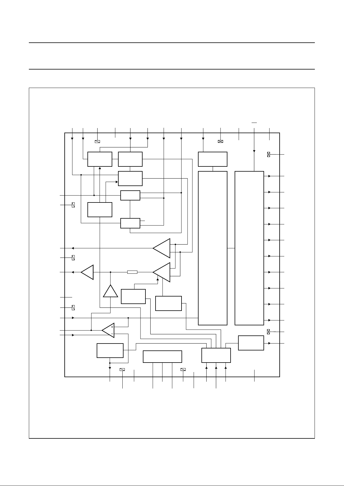
BLOCK DIAGRAM
handbook, full pagewidth
MGM505
TRACK-
AND-HOLD
TRACK-
AND-HOLD
TRACK-
AND-HOLD
CLAMP
ref1
CLAMP
8-BIT DAC
10-BIT DAC
9-BIT DAC
6 dB
AGC
1
1
CLOCK
GENERATOR
10-BIT ADC
REGULATOR
SERIAL
INTERFACE
4-BIT DAC
CUT-OFF
OUTPUTS
BUFFER
5
4
2
7
6
9
10
14
11
12
13 15 16 17 18
20
21
22
2319
24
36
3
25
26
27
28
29
30
31
32
33
34
35
3738394041424344
454846
47
IND INP AGND3 SHD SHP CLPDM CLK
DGND2
V
CCO
V
CCD2
V
CCA3
OE
D9
D8
D7
D6
D5
D4
D3
D2
D1
D0
DGND1
OFDOUT
OGND
V
CCD1
STDBY
SENAGND6
SCLK
SDATA
DEC1
V
RT
V
RB
V
CCA2
DACOUT
V
ref
CLPADC
AGND2
ADCIN
AGND5
V
CCA1
AGCOUT
AGND4
AGND1
8
CPCDS
AMPOUT
TDA8784
4-BIT DAC
CUT-OFF
1
CLPOB
Fig.1 Block diagram.
Page 5

1999 Sep 21 5
Philips Semiconductors Product specification
18 Msps, 10-bit analog-to-digital
interface for CCD cameras
TDA8784
PINNING
SYMBOL PIN DESCRIPTION
CLPOB 1 clamp pulse input at optical black
AGND4 2 analog ground 4
OFDOUT 3 analog output of the additional 8-bit control DAC (controlled via the serial interface)
AMPOUT 4 CDS amplifier output (fixed gain = 6 dB)
AGND1 5 analog ground 1
V
CCA1
6 analog supply voltage 1
AGCOUT 7 AGC amplifier signal output
CPCDS 8 clamp storage capacitor pin
AGND5 9 analog ground5
ADCIN 10 ADC analog signal input from AGCOUT via a short circuit
CLPADC 11 clamp control input for ADC analog input signal clamp (used with a capacitor from V
ref
to ground)
V
ref
12 ADC input clamp reference voltage (normally connected to pin VRB or DACOUT, or shorted to
ground via a capacitor)
DACOUT 13 DAC output for ADC clamp level
AGND2 14 analog ground 2
V
CCA2
15 analog supply voltage 2
V
RB
16 ADC reference voltage (BOTTOM) code 0
V
RT
17 ADC reference voltage (TOP) code 1023
DEC1 18 decoupling 1 (decoupled to ground via a capacitor)
AGND6 19 analog ground 6
SDATA 20 serial data input for the 4 control DACs (9-bit DAC for AGC gain, 8-bit DAC for frequency cut-off;
additional 8-bit DAC for OFD output voltage; 10-bit DACforADC clamp level and the standby mode
per block and edge pulse control); see Table 1
SCLK 21 serial clock input for the control DACs and their serial interface; see Table 1
SEN 22 enable input for the serial interface shift register (active when SEN = logic 0); see Table 1
STDBY 23 standby control pin (active HIGH); all the output bits are logic 0 when standby is enabled
V
CCD1
24 digital supply voltage 1
DGND1 25 digital ground 1
D0 26 ADC digital output 0 (LSB)
D1 27 ADC digital output 1
D2 28 ADC digital output 2
D3 29 ADC digital output 3
D4 30 ADC digital output 4
D5 31 ADC digital output 5
D6 32 ADC digital output 6
D7 33 ADC digital output 7
D8 34 ADC digital output 8
D9 35 ADC digital output 9 (MSB)
OGND 36 digital output ground
V
CCO
37 digital output supply voltage
Page 6
1999 Sep 21 6
Philips Semiconductors Product specification
18 Msps, 10-bit analog-to-digital
interface for CCD cameras
TDA8784
OE 38 output enable (active LOW: digital outputs active; active HIGH: digital outputs high impedance)
V
CCD2
39 digital supply voltage 2
DGND2 40 digital ground 2
CLK 41 ADC clock input
CLPDM 42 clamp pulse input at dummy pixel
SHP 43 pre-set sample-and-hold pulse input
SHD 44 data sample-and-hold pulse input
V
CCA3
45 analog supply voltage 3
INP 46 pre-set input signal from CCD
IND 47 data input signal from CCD
AGND3 48 analog ground 3
SYMBOL PIN DESCRIPTION
Fig.2 Pin configuration.
1
2
3
4
5
6
7
8
9
10
11
36
35
34
33
32
31
30
29
28
27
26
13
14
15
16
17
18
19
20
21
22
23
48
47
46
45
44
43
42
41
40
39
38
12
24 37
25
TDA8784H
MGM506
OGND
D9
D8
D7
D5
D4
D3
D2
D1
D0
DGND1
CLPOB
AGND4
OFDOUT
AMPOUT
AGND1
V
CCA1
CPCDS
AGND5
CLPADC
V
ref
D6
IND
INP
V
CCA3
SHD
SHP
CLPDM
DGND2
V
CCD2
OE
V
CCO
AGND3
CLK
AGCOUT
ADCIN
AGND2
V
CCA2
V
RB
V
RT
DEC1
AGND6
SDATA
SEN
STDBY
V
CCD1
DACOUT
SCLK
Page 7
1999 Sep 21 7
Philips Semiconductors Product specification
18 Msps, 10-bit analog-to-digital
interface for CCD cameras
TDA8784
LIMITING VALUES
In accordance with the Absolute Maximum Rating System (IEC 134).
Note
1. The supply voltages V
CCA
, V
CCD
and V
CCO
may have any value between −0.3 and +7.0 V provided that the supply
voltage difference ∆VCC remains as indicated.
HANDLING
Inputs and outputs are protected against electrostatic discharges in normal handling. However, to be totally safe, it is
desirable to take normal precautions appropriate to handling integrated circuits.
THERMAL CHARACTERISTICS
SYMBOL PARAMETER CONDITIONS MIN. MAX. UNIT
V
CCA
analog supply voltage note 1 −0.3 +7.0 V
V
CCD
digital supply voltage note 1 −0.3 +7.0 V
V
CCO
output stages supply voltage note 1 −0.3 +7.0 V
∆V
CC
supply voltage difference
between V
CCA
and V
CCD
−1.0 +1.0 V
between V
CCA
and V
CCO
−1.0 +4.0 V
between V
CCD
and V
CCO
−1.0 +4.0 V
V
i
input voltage referenced to AGND −0.3 +7.0 V
V
CLK(p-p)
AC input voltage for switching
(peak-to-peak value)
referenced to DGND − V
CCD
V
I
o
output current − 10 mA
T
stg
storage temperature −55 +150 °C
T
amb
ambient temperature −20 +75 °C
T
j
junction temperature − 150 °C
SYMBOL PARAMETER CONDITIONS VALUE UNIT
R
th(j-a)
thermal resistance from junction to ambient in free air 76 K/W
Page 8
1999 Sep 21 8
Philips Semiconductors Product specification
18 Msps, 10-bit analog-to-digital
interface for CCD cameras
TDA8784
CHARACTERISTICS
V
CCA=VCCD
=5V; V
CCO
=3V; f
CLK
= 18 MHz; T
amb
=25°C; unless otherwise specified.
SYMBOL PARAMETER CONDITIONS MIN. TYP. MAX. UNIT
Supplies
V
CCA
analog supply voltage 4.75 5 5.25 V
V
CCD
digital supply voltage 4.75 5 5.25 V
V
CCO
digital outputs supply voltage 2.5 3 5.25 V
I
CCA
analog supply current − 78 85 mA
I
CCD
digital supply current − 18 20 mA
I
CCO
digital outputs supply current CL= 20 pF on all data outputs;
ramp input
− 1 − mA
Digital inputs
C
LOCK INPUT: CLK (REFERENCED TO DGND)
V
IL
LOW-level input voltage 0 − 0.8 V
V
IH
HIGH-level input voltage 2.0 − V
CCD
V
I
IL
LOW-level input current V
CLK
= 0.8 V −1 − +1 µA
I
IH
HIGH-level input current V
CLK
= 2.0 V −−20 µA
Z
i
input impedance f
CLK
= 18 MHz − 46 − kΩ
C
i
input capacitance f
CLK
= 18 MHz − 1 − pF
INPUTS: SHP AND SHD
V
IL
LOW-level input voltage 0 − 0.8 V
V
IH
HIGH-level input voltage 2.0 − V
CCD
V
I
IL
LOW-level input current VIL= 0.6 V −−6−µA
I
IH
HIGH-level input current VIH= 2.2 V − 0 −µA
INPUTS: SEN, SCLK, SDATA, OE, STDBY, CLPDM, CLPOB AND CLPADC
V
IL
LOW-level input voltage 0 − 0.8 V
V
IH
HIGH-level input voltage 2.0 − V
CCD
V
I
i
input current −2 − +2 µA
Correlated Double Sampling (CDS)
V
i(CDS)(p-p)
CDS input amplitude
(peak-to-peak value)
− 400 1200 mV
I
CPCDS,INP,IND
input current pins 8, 46
and 47
−2 − +2 µA
t
CDS(min)
CDS control pulses minimum
active time
f
i(CDS1,2)=fCLK(pix);
V
i(CDS)
= 1200 mV (p-p)
black-to-white transition in
1 pixel (±1 LSB typ.);
f
cut(CDS)
= 40 MHz;
f
cut(AGC)
= 40 MHz
12 −−ns
t
hd1
hold time INP compared to
control pulse SHP
see Fig.5 − 1 − ns
Page 9
1999 Sep 21 9
Philips Semiconductors Product specification
18 Msps, 10-bit analog-to-digital
interface for CCD cameras
TDA8784
t
hd2
hold time of IND compared to
control pulse SHD
see Fig.5 − 1 − ns
t
set(CDS)
CDS settling time see Fig.12; control DAC 4 bits
input code; AGC gain=0dB;
f
cut(AGC)
= 54 MHz;
V
i(CDS)
= 1200 mV (p-p)
black-to-white transition in 1
pixel (1 LSB typ.)
0000 − 12 − ns
0001 − 25 − ns
0010 − 45 − ns
0011 − 55 − ns
0100 − 105 − ns
0111 − 140 − ns
1000 − 270 − ns
1011 − 300 − ns
1111 − 365 − ns
Amplifier outputs
G
AMPOUT
output amplifier gain − 6 − dB
Z
AMPOUT
output amplifier impedance − 300 −Ω
V
AMPOUT(p-p)
output amplifier dynamic
voltage (peak-to-peak value)
− 2.4 − V
V
AMPOUT(bl)
output amplifier black level
voltage
− 1.5 − V
V
AGCOUT(p-p)
AGCoutputamplifierdynamic
voltage level (peak-to-peak
value)
− 2000 − mV
V
AGCOUT
AGC output amplifier
black level voltage
V
ref
connected to DACOUT − V
ref
− V
Z
AGCOUT
AGC output amplifier output
impedance
at 10 kHz − 5 −Ω
I
AGCOUT
AGC output static drive
current
static −−1mA
G
AGC(min)
minimum gain of AGC circuit AGC DAC input code = 00
(9-bit control)
− 4.5 − dB
G
AGC(max)
maximum gain of AGC circuit AGC DAC input code≥319
(9-bit control)
− 34.5 − dB
f
cut(AGC)
cut-off frequency AGC control DAC 4-bit
input code = 00 − 54 − MHz
input code = 01 − 40 − MHz
input code = 15 − 4 − MHz
SYMBOL PARAMETER CONDITIONS MIN. TYP. MAX. UNIT
Page 10

1999 Sep 21 10
Philips Semiconductors Product specification
18 Msps, 10-bit analog-to-digital
interface for CCD cameras
TDA8784
Clamps
g
m(ADC)
ADC clamp transconductance at clamp level − 7 − mS
g
m(CDS)
CDS clamp transconductance at clamp level − 1.5 − mS
Analog-to-Digital Converter (ADC)
f
CLK(max)
maximum clock frequency 18 −−MHz
t
CPH
clock pulse width HIGH 15 −−ns
t
CPL
clock pulse width LOW 15 −−ns
SR
CLK
clock input slew rate (rising
and falling edge)
10% to 90% 0.5 −−V/ns
V
i(ADC)(p-p)
ADC input voltage level
(peak-to-peak value)
− 2 − V
V
RB
ADC reference voltage output
code 0
− 1.5 − V
V
RT
ADC reference voltage output
code 1023
− 3.5 − V
I
ADCIN
input current pin 10 −2 − +120 µA
INL integral non-linearity ramp input −±0.6 ±1.5 LSB
DNL differential non-linearity ramp input −±0.2 ±0.75 LSB
t
d(s)
sampling delay time −−5ns
Total chain characteristics (CDS + AGC + ADC)
t
d
time delay between
SHD and CLK
see Fig.5; 50% at rising
edges CLK and SHP: transition
full scale code 0 to 1023;
f
cut(CDS)
= 40 MHz;
f
cut(AGC)
= 40 MHz;
V
i(CDS)
= 1200 mV
− 40 − ns
N
tot(rms)
total output noise (RMS
value)
f
cut(CDS)
= 120 MHz;
f
cut(AGC)
= 40 MHz; note 1
G
AGC
= 4.5 dB − 0.125 − LSB
G
AGC
= 34.5 dB − 1.6 − LSB
V
offset(fl-d)
maximum offset between
CCD floating level and CCD
dark pixel level
−200 − +200 mV
V
n(i)(eq)(rms)
equivalent input noise voltage
(RMS value)
AGC gain = 34.5 dB − 125 −µV
AGC gain = 4.5 dB − 150 −µV
Digital-to-analog converter (OFDOUT)
V
OFDOUT(p-p)
additional 8-bit control DAC
(OFD) output voltage
(peak-to-peak value)
− 1.4 − V
V
OFDOUT(0)
DC output voltage for code 0 − 2.3 − V
V
OFDOUT(255)
DC output voltage for
code 255
− 3.7 − V
SYMBOL PARAMETER CONDITIONS MIN. TYP. MAX. UNIT
Page 11

1999 Sep 21 11
Philips Semiconductors Product specification
18 Msps, 10-bit analog-to-digital
interface for CCD cameras
TDA8784
Note
1. Noisemeasurementat ADC outputs: the coupling capacitor at the input is connectedtoground, so that only the noise
contributionofthefront-endisevaluated.Thefront-endoperatesat18 Mpix with a line of 1024 pixels. The first 40 are
used to run CLPOB and the last 40 to run CLPDM. Data at the ADC outputs is measured during the other pixels.
The differences between the types of codes statistic is then computed; the result is the noise. No quantization noise
is taken into account as no signal is input.
Z
OFDOUT
additional 8-bit control DAC
(OFD) output impedance
− 2000 −Ω
I
OFDOUT
OFD output current drive static −−50 µA
ADC clamp control DAC (see Fig.8)
V
DACOUT(p-p)
ADC clamp 10-bit control
DAC output voltage
(peak-to-peak value)
− 1 − V
V
DACOUT
DC output voltage code 0 − 1.5 − V
code 1023 − 2.5 − V
Z
DACOUT
ADC clamp control DAC
output impedance
−−250 Ω
I
DACOUT
DAC output current drive static −−50 µA
OFE
LOOP
maximum offset error of
DAC+ ADC clamp loop
code 0 −±5−LSB
code 1023 −±5−LSB
Digital outputs (f
CLK
= 18 MHz; CL=20pF)
V
OH
HIGH-level output voltage IOH= −1mA V
CCO
− 0.5 − V
CCO
V
V
OL
LOW-level output voltage IOL=1mA 0 − 0.5 V
I
OZ
output current in 3-state mode 0V<Vo<V
CCO
−20 − +20 µA
t
o(h)
output hold time see Fig.5 8 −−ns
t
o(d)
output delay time Ci= 20 pF; V
CCO
=5V − 17 23 ns
C
i
=10pF − 15 21 ns
C
i
= 20 pF; V
CCO
=3V − 20 29 ns
C
i
=10pF − 17 25 ns
C
i
= 20 pF; V
CCO
= 2.5 V − 22 33 ns
C
i
=10pF − 18 28 ns
Serial interface
f
SCLK(max)
maximum frequency of serial
interface
5 −−MHz
SYMBOL PARAMETER CONDITIONS MIN. TYP. MAX. UNIT
Page 12

1999 Sep 21 12
Philips Semiconductors Product specification
18 Msps, 10-bit analog-to-digital
interface for CCD cameras
TDA8784
Fig.3 Serial interface block diagram.
handbook, full pagewidth
OFD
LATCHES
AGC GAIN
LATCHES
FREQUENCY
LATCHES
PARTIAL
STANDBY
AND EDGE
CLAMP
REFERENCE
LATCHES
LATCH
SELECTION
D0
LSB MSB
SDATA
SCLK
SEN
8-bit DAC 10-bit DAC
MGM515
AGC control frequency
control
CDS and AGC
standby
control
or edge clocks
D1 D2 D3 D4 D510D6
SHIFT REGISTER
D7 D8 D9 A0 A1 A2
8
(D7 to D0)
8
(D7 to D0)
8
(D7 to D0)
7
(D6 to D0)
10
(D9 to D0)
Fig.4 Loading sequence of control DACs input data via the serial interface.
handbook, full pagewidth
MGE373
A2SDATA
SCLK
SEN
A1 A0 D9 D7 D6 D5 D4 D3
MSB LSB
D2 D1 D0
t
hd3
t
su3
t
su1
t
hd4
t
su2
D8
t
su1=tsu2
= 4 ns (min.); t
hd3=thd4
= 4 ns (min.).
Page 13

1999 Sep 21 13
Philips Semiconductors Product specification
18 Msps, 10-bit analog-to-digital
interface for CCD cameras
TDA8784
Table 1 Serial interface programming
Note
1. When CLPADC is HIGH (D4 = 1: serial interface), the ADC input is clamped to voltage level V
ref
.
V
ref
is connected to ground via a capacitance.
Table 2 Standby selection
ADDRESS BITS
DATA BITS D9 to D0
A2 A1 A0
0 0 0 OFD output control (D7 to D0).
0 0 1 Cut-off frequency of CDS and AGC. Only the 4 LSBs (D3 to D0) are used for
CDS. D4 to D7 are used for AGC. D8 and D9 should be set to logic 0.
0 1 0 AGC gain control (D8 to D0).
0 1 1 Partial standby controls for power consumption optimization. Only the 4 LSBs
(D3 to D0) are used. Edge control for pulses SHP, SHD, CLAMP and
clock ADC:
D0 = 1: CDS + AGC in standby; I
CCA+ICCD
=48mA
D1 = 1: OFD DAC in standby; I
CCA+ICCD
=98mA
D2 = 1: 6 dB amplifier (output on AMPOUT pin) in standby;
I
CCA+ICCD
= 98.5 mA
D3 = 1: SHP and SHD activated with falling edge (for positive pulse)
D4 = 1: CLPDM, CLPOB and CLPADC activated on HIGH level; note 1
D5 = 0: CLKADC activated with falling edge
D6 must be set to logic 0.
1 0 0 Clamp reference DAC (D9 to D0).
STDBY DATA BITS D9 to D0 I
CCA+ICCD
(TYP.)
1LOW4mA
0 active 99 mA
Page 14

1999 Sep 21 14
Philips Semiconductors Product specification
18 Msps, 10-bit analog-to-digital
interface for CCD cameras
TDA8784
handbook, full pagewidth
MGR395
N
INP
and
IND
SHP 1.4 V
SHD
CLK
ADC
DATA
N + 3N + 2N + 1
N − 1
N
N
t
CDS
t
CPH
t
d(s)
t
d
t
o(d)
t
o(h)
t
hd1
t
hd2
90%
10%
1.4 V
1.4 V
Fig.5 Pixel frequency timing diagram.
Page 15

1999 Sep 21 15
Philips Semiconductors Product specification
18 Msps, 10-bit analog-to-digital
interface for CCD cameras
TDA8784
Fig.6 Line frequency timing diagram.
(1) When dummy pixels are not available.
handbook, full pagewidth
MGR396
CLPADC
(active HIGH)
CLPDM
(active HIGH)
CLPOB
(active HIGH)
OPTICAL BLACK HORIZONTAL FLYBLACK DUMMY VIDEOVIDEOAGCOUT
CLPDM2
CLPADC
WINDOW
CLPDB
WINDOW
(1)
(1)
1 pixel
CLPDMR
CLPADC
WINDOW
1 pixel
Page 16

1999 Sep 21 16
Philips Semiconductors Product specification
18 Msps, 10-bit analog-to-digital
interface for CCD cameras
TDA8784
handbook, halfpage
MGM507
G
AGC
(dB)
34.5
4.5
0 319
511
AGC control DAC input code
Fig.7 AGC gain as a function of DAC input code.
Fig.8 DAC voltage output as a function of DAC input code.
handbook, full pagewidth
0
ADC CLAMP DAC
voltage
output
(V)
2.5
1.5
1023
ADC CLAMP control DAC input code
MGM508
0
OFD DAC
voltage
output
(V)
3.4
2.0
255
OFD control DAC input code
Fig.8 DAC voltage output as a function of DAC input code.
Page 17

1999 Sep 21 17
Philips Semiconductors Product specification
18 Msps, 10-bit analog-to-digital
interface for CCD cameras
TDA8784
Fig.9 Typical clamp current for pin CPCDS.
handbook, halfpage
MGR397
+100
0
−100
I
(µA)
V (V)
200 mV
2.85
Fig.10 Typical clamp current for pins IND and INP.
handbook, halfpage
MGR398
+300
0
−300
I
(µA)
V (V)
400 mV
2.85
Fig.11 Typical clamp current for pin V
ref
.
handbook, halfpage
MGR399
+200
0
−200
I
(µA)
V (V)
400 mV
V
ref
Fig.11 Typical clamp current for pin V
ref
.
Page 18

1999 Sep 21 18
Philips Semiconductors Product specification
18 Msps, 10-bit analog-to-digital
interface for CCD cameras
TDA8784
Fig.12 CDS settling time and bandwidth.
handbook, full pagewidth
160
120
40
0
80
MGR400
F05A16B27C38D49E
4-bit control DAC input code
f
cut
(MHz)
400
300
100
0
200
t
set
(ns)
(2)
(3)
(4)
(1)
(1) f
cut
.
(2) t
set
(10b).
(3) t
set
(9b).
(4) t
set
(8b).
Page 19

1999 Sep 21 19
Philips Semiconductors Product specification
18 Msps, 10-bit analog-to-digital
interface for CCD cameras
TDA8784
Fig.13 AGC bandwidth.
handbook, full pagewidth
F
60
40
20
0
05A16B27C38D49E
MGR401
4-bit control DAC input code
f
cut
(MHz)
Fig.13 AGC bandwidth.
Fig.14 CDS output.
handbook, full pagewidth
1.6
1.6
1.2
0.4
0
0 0.4 1.2
0.8
0.80.2 0.6 1.41.0
MGR402
V
i(CDS)(p-p)
(V)
V
o(CDS)(p-p)
(V)
t
set(CDS)
=12ns.
Fig.14 CDS output.
t
set(CDS)
=12ns.
Page 20

1999 Sep 21 20
Philips Semiconductors Product specification
18 Msps, 10-bit analog-to-digital
interface for CCD cameras
TDA8784
Fig.15 Output noise (RMS value).
handbook, full pagewidth
13F
code
3
2
1
0
00 40 80 C0 100
(34.5)(4.5) (10.5) (16.5) (22.5) (28.5)
MGR403
G
AGC
(dB)
N
tot(rms)
(LSB)
(2)
(3)
(4)
(5)
(1)
(1) f
pix
= 18 MHz; control DAC = 10H; f
cut(CDS)
= 120 MHz; f
cut(AGC)
= 40 MHz.
(2) f
pix
= 10 MHz; control DAC = 31H; f
cut(CDS)
= 80 MHz; f
cut(AGC)
= 30 MHz.
(3) f
pix
= 5 MHz; control DAC = 43H; f
cut(CDS)
= 35 MHz; f
cut(AGC)
= 12 MHz.
(4) f
pix
= 1 MHz; control DAC = F8H; f
cut(CDS)
= 6 MHz; f
cut(AGC)
= 4 MHz.
(5) f
pix
= 375 kHz; control DAC = FFH; f
cut(CDS)
= 4 MHz; f
cut(AGC)
= 4 MHz.
Fig.15 Output noise (RMS value).
Page 21

1999 Sep 21 21
Philips Semiconductors Product specification
18 Msps, 10-bit analog-to-digital
interface for CCD cameras
TDA8784
APPLICATION INFORMATION
handbook, full pagewidth
MGM516
1
2
3
4
5
6
7
8
9
10
11
36
48 47 46 45 44 43 42 41 40 39 38 37
13 14 15 16 17 18 19 20 21 22 23 24
35
34
33
32
31
30
29
28
27
26
12
25
TDA8784
OGND
D9
D8
D7
D5
D4
D3
D2
D1
D0
DGND1
CLPOB
AGND4
OFDOUT
AMPOUT
AGND1
V
CCA1
CPCDS
AGND5
CLPADC
V
ref
D6
IND
INP
V
CCA3
SHD
SHP
CLPDM
DGND2
V
CCD2
OE
V
CCO
AGND3
CLK
AGCOUT
ADCIN
AGND2
V
CCA2
V
RB
V
RT
DEC1
AGND6
SDATA
SEN
STDBY
V
CCD1
DACOUT
SCLK
from timing
generator
serial
interface
5.0 V 5.0 V
5.0 V
5.0 V
CCD
2.5 to 5.25 V
(3)
1 µF
1 µF
(3)
(3)
(2)
(1)
(3)
5.0 V
(3)
100
nF
1
nF
2.2
nF
1
nF
(3)
1 µF
Fig.16 Application diagram.
Depending on the application, the following connections must be made:
(1) The clamp level of the signal input at ADCIN can be tuned from code 00 to code 511 in 0.5 LSB steps of ADC via the serial interface
(clamp ADC activated).
(2) Clamp ADC not activated, direct connection from DACOUT to V
ref
.
(3) All supply pins must be decoupled with 100 nF capacitors as close as possible to the device.
Page 22

1999 Sep 21 22
Philips Semiconductors Product specification
18 Msps, 10-bit analog-to-digital
interface for CCD cameras
TDA8784
Power and grounding recommendations
When designing a printed-circuit board for applications
such as PC cameras, surveillance cameras, camcorders
and digital still cameras, care should be taken to minimize
the noise.
For the front-end integrated circuit, the basic rules of
printed-circuit board design and implementation of
analogue components (such as classical operational
amplifiers) must be respected, particularly with respect to
power and ground connections.
The following additional recommendation is given for the
CDS input pin(s) which is/are internally connected to the
programmable gain amplifier:
• The connections between CCD interfaceandCDS input
should be as short as possible and a ground ring
protection around these connections can be beneficial.
Separate analogue and digital supplies providethe best
solution. If it is not possible to do this on the board then
the analogue supply pins must be decoupled effectively
from the digital supply pins. If the same power supply
and ground are used for all the pins then the decoupling
capacitors must be placed as close as possible to the IC
package.
• In a two-ground system, in order to minimize the noise
though package and die parasitics, the following
recommendations must be implemented:
– All the analogue and digital supply pins must be
decoupled to the analogue ground plane. Only the
groundpinassociatedwiththe digital outputs must be
connected to the digital ground plane. All the other
ground pins should be connected to the analogue
ground plane. The analogue and digital ground
planes must be connected together at one point as
close as possible to the ground pin associated with
the digital outputs.
– The digital output pins and their associated lines
should be shielded by the digital ground plane which
can be used then as return path for digital signals.
Page 23

1999 Sep 21 23
Philips Semiconductors Product specification
18 Msps, 10-bit analog-to-digital
interface for CCD cameras
TDA8784
PACKAGE OUTLINE
UNIT
A
max.
A1A2A3b
p
cE
(1)
eH
E
LL
p
Zywv θ
REFERENCES
OUTLINE
VERSION
EUROPEAN
PROJECTION
ISSUE DATE
IEC JEDEC EIAJ
mm
1.60
0.20
0.05
1.45
1.35
0.25
0.27
0.17
0.18
0.12
7.1
6.9
0.5
9.15
8.85
0.95
0.55
7
0
o
o
0.12 0.10.21.0
DIMENSIONS (mm are the original dimensions)
Note
1. Plastic or metal protrusions of 0.25 mm maximum per side are not included.
0.75
0.45
SOT313-2
94-12-19
97-08-01
D
(1) (1)(1)
7.1
6.9
H
D
9.15
8.85
E
Z
0.95
0.55
D
b
p
e
E
B
12
D
H
b
p
E
H
v M
B
D
Z
D
A
Z
E
e
v M
A
1
48
37
36
25
24
13
θ
A
1
A
L
p
detail X
L
(A )
3
A
2
X
y
c
w M
w M
0 2.5 5 mm
scale
pin 1 index
LQFP48: plastic low profile quad flat package; 48 leads; body 7 x 7 x 1.4 mm
SOT313-2
Page 24

1999 Sep 21 24
Philips Semiconductors Product specification
18 Msps, 10-bit analog-to-digital
interface for CCD cameras
TDA8784
SOLDERING
Introduction to soldering surface mount packages
Thistextgivesaverybriefinsighttoacomplextechnology.
A more in-depth account of soldering ICs can be found in
our
“Data Handbook IC26; Integrated Circuit Packages”
(document order number 9398 652 90011).
There is no soldering method that is ideal for all surface
mount IC packages. Wave soldering is not always suitable
for surface mount ICs, or for printed-circuit boards with
high population densities. In these situations reflow
soldering is often used.
Reflow soldering
Reflow soldering requires solder paste (a suspension of
fine solder particles, flux and binding agent) to be applied
totheprinted-circuitboard by screen printing, stencilling or
pressure-syringe dispensing before package placement.
Several methods exist for reflowing; for example,
infrared/convection heating in a conveyor type oven.
Throughput times (preheating, soldering and cooling) vary
between 100 and 200 seconds depending on heating
method.
Typical reflow peak temperatures range from
215 to 250 °C. The top-surface temperature of the
packages should preferable be kept below 230 °C.
Wave soldering
Conventional single wave soldering is not recommended
forsurfacemountdevices(SMDs)orprinted-circuitboards
with a high component density, as solder bridging and
non-wetting can present major problems.
To overcome these problems the double-wave soldering
method was specifically developed.
If wave soldering is used the following conditions must be
observed for optimal results:
• Use a double-wave soldering method comprising a
turbulent wave with high upward pressure followed by a
smooth laminar wave.
• For packages with leads on two sides and a pitch (e):
– larger than or equal to 1.27 mm, the footprint
longitudinal axis is preferred to be parallel to the
transport direction of the printed-circuit board;
– smaller than 1.27 mm, the footprint longitudinal axis
must be parallel to the transport direction of the
printed-circuit board.
The footprint must incorporate solder thieves at the
downstream end.
• Forpackageswithleadsonfoursides,thefootprintmust
be placed at a 45° angle to the transport direction of the
printed-circuit board. The footprint must incorporate
solder thieves downstream and at the side corners.
During placement and before soldering, the package must
be fixed with a droplet of adhesive. The adhesive can be
applied by screen printing, pin transfer or syringe
dispensing. The package can be soldered after the
adhesive is cured.
Typical dwell time is 4 seconds at 250 °C.
A mildly-activated flux will eliminate the need for removal
of corrosive residues in most applications.
Manual soldering
Fix the component by first soldering two
diagonally-opposite end leads. Use a low voltage (24 V or
less) soldering iron applied to the flat part of the lead.
Contact time must be limited to 10 seconds at up to
300 °C.
When using a dedicated tool, all other leads can be
soldered in one operation within 2 to 5 seconds between
270 and 320 °C.
Page 25

1999 Sep 21 25
Philips Semiconductors Product specification
18 Msps, 10-bit analog-to-digital
interface for CCD cameras
TDA8784
Suitability of surface mount IC packages for wave and reflow soldering methods
Notes
1. All surface mount (SMD) packages are moisture sensitive. Depending upon the moisture content, the maximum
temperature (with respect to time) and body size of the package, there is a risk that internal or external package
cracks may occur due to vaporization of the moisture in them (the so called popcorn effect). For details, refer to the
Drypack information in the
“Data Handbook IC26; Integrated Circuit Packages; Section: Packing Methods”
.
2. These packages are not suitable for wave soldering as a solder joint between the printed-circuit board and heatsink
(at bottom version) can not be achieved, and as solder may stick to the heatsink (on top version).
3. If wave soldering is considered, then the package must be placed at a 45° angle to the solder wave direction.
The package footprint must incorporate solder thieves downstream and at the side corners.
4. Wave soldering is only suitable for LQFP, TQFP and QFP packages with a pitch (e) equal to or larger than 0.8 mm;
it is definitely not suitable for packages with a pitch (e) equal to or smaller than 0.65 mm.
5. Wave soldering is only suitable for SSOP and TSSOP packages with a pitch (e) equal to or larger than 0.65 mm; it is
definitely not suitable for packages with a pitch (e) equal to or smaller than 0.5 mm.
DEFINITIONS
LIFE SUPPORT APPLICATIONS
These products are not designed for use in life support appliances, devices, or systems where malfunction of these
products can reasonably be expected to result in personal injury. Philips customers using or selling these products for
use in such applications do so at their own risk and agree to fully indemnify Philips for any damages resulting from such
improper use or sale.
PACKAGE
SOLDERING METHOD
WAVE REFLOW
(1)
BGA, SQFP not suitable suitable
HLQFP, HSQFP, HSOP, HTQFP, HTSSOP, SMS not suitable
(2)
suitable
PLCC
(3)
, SO, SOJ suitable suitable
LQFP, QFP, TQFP not recommended
(3)(4)
suitable
SSOP, TSSOP, VSO not recommended
(5)
suitable
Data sheet status
Objective specification This data sheet contains target or goal specifications for product development.
Preliminary specification This data sheet contains preliminary data; supplementary data may be published later.
Product specification This data sheet contains final product specifications.
Limiting values
Limiting values given are in accordance with the Absolute Maximum Rating System (IEC 134). Stress above one or
more of the limiting values may cause permanent damage to the device. These are stress ratings only and operation
of the device at these or at any other conditions above those given in the Characteristics sections of the specification
is not implied. Exposure to limiting values for extended periods may affect device reliability.
Application information
Where application information is given, it is advisory and does not form part of the specification.
Page 26

1999 Sep 21 26
Philips Semiconductors Product specification
18 Msps, 10-bit analog-to-digital
interface for CCD cameras
TDA8784
NOTES
Page 27

1999 Sep 21 27
Philips Semiconductors Product specification
18 Msps, 10-bit analog-to-digital
interface for CCD cameras
TDA8784
NOTES
Page 28

© Philips Electronics N.V. SCA
All rights are reserved. Reproduction in whole or in part is prohibited without the prior written consent of the copyright owner.
The information presented in this document does not form part of any quotation or contract, is believed to be accurate and reliable and may be changed
without notice. No liability will be accepted by the publisher for any consequence of its use. Publication thereof does not convey nor imply any license
under patent- or other industrial or intellectual property rights.
Internet: http://www.semiconductors.philips.com
1999
68
Philips Semiconductors – a w orldwide compan y
For all other countries apply to: Philips Semiconductors,
International Marketing & Sales Communications, Building BE-p, P.O. Box 218,
5600 MD EINDHOVEN, The Netherlands, Fax. +31 40 27 24825
Argentina: see South America
Australia: 3 Figtree Drive, HOMEBUSH, NSW 2140,
Tel. +61 2 9704 8141, Fax. +61 2 9704 8139
Austria: Computerstr. 6, A-1101 WIEN, P.O. Box 213,
Tel. +43 1 60 101 1248, Fax. +43 1 60 101 1210
Belarus: Hotel Minsk Business Center, Bld. 3, r. 1211, Volodarski Str. 6,
220050 MINSK, Tel. +375 172 20 0733, Fax. +375 172 20 0773
Belgium: see The Netherlands
Brazil: seeSouth America
Bulgaria: Philips Bulgaria Ltd., Energoproject, 15thfloor,
51 James Bourchier Blvd., 1407 SOFIA,
Tel. +359 2 68 9211, Fax. +359 2 68 9102
Canada: PHILIPS SEMICONDUCTORS/COMPONENTS,
Tel. +1 800 234 7381, Fax. +1 800 943 0087
China/Hong Kong: 501 Hong Kong Industrial Technology Centre,
72 Tat Chee Avenue, Kowloon Tong, HONG KONG,
Tel. +852 2319 7888, Fax. +852 2319 7700
Colombia: see South America
Czech Republic: see Austria
Denmark: Sydhavnsgade 23, 1780 COPENHAGEN V,
Tel. +45 33 29 3333, Fax. +45 33 29 3905
Finland: Sinikalliontie 3, FIN-02630 ESPOO,
Tel. +358 9 615 800, Fax. +358 9 6158 0920
France: 51 Rue Carnot, BP317, 92156 SURESNES Cedex,
Tel. +33 1 4099 6161, Fax. +33 1 4099 6427
Germany: Hammerbrookstraße 69, D-20097 HAMBURG,
Tel. +49 40 2353 60, Fax. +49 40 2353 6300
Hungary: seeAustria
India: Philips INDIA Ltd, Band Box Building, 2nd floor,
254-D, Dr. Annie Besant Road, Worli, MUMBAI 400 025,
Tel. +91 22 493 8541, Fax. +91 22 493 0966
Indonesia: PT Philips DevelopmentCorporation, SemiconductorsDivision,
Gedung Philips, Jl. Buncit Raya Kav.99-100, JAKARTA 12510,
Tel. +62 21 794 0040 ext. 2501, Fax. +62 21 794 0080
Ireland: Newstead, Clonskeagh, DUBLIN 14,
Tel. +353 1 7640 000, Fax. +353 1 7640 200
Israel: RAPAC Electronics, 7 Kehilat Saloniki St, PO Box 18053,
TEL AVIV 61180, Tel. +972 3 645 0444, Fax. +972 3 649 1007
Italy: PHILIPS SEMICONDUCTORS,Via Casati, 23 - 20052 MONZA (MI),
Tel. +39 039 203 6838, Fax +39 039 203 6800
Japan: Philips Bldg 13-37, Kohnan 2-chome, Minato-ku,
TOKYO 108-8507, Tel. +81 3 3740 5130, Fax. +81 3 3740 5057
Korea: Philips House, 260-199 Itaewon-dong, Yongsan-ku, SEOUL,
Tel. +82 2 709 1412, Fax. +82 2 709 1415
Malaysia: No. 76 Jalan Universiti, 46200 PETALING JAYA, SELANGOR,
Tel. +60 3 750 5214, Fax. +60 3 757 4880
Mexico: 5900 Gateway East, Suite 200, EL PASO, TEXAS 79905,
Tel. +9-5 800 234 7381, Fax +9-5 800 943 0087
Middle East: see Italy
Netherlands: Postbus 90050, 5600 PB EINDHOVEN, Bldg. VB,
Tel. +31 40 27 82785, Fax. +31 40 27 88399
New Zealand: 2 Wagener Place, C.P.O. Box 1041, AUCKLAND,
Tel. +64 9 849 4160, Fax. +64 9 849 7811
Norway: Box 1, Manglerud 0612, OSLO,
Tel. +47 22 74 8000, Fax. +47 22 74 8341
Pakistan: see Singapore
Philippines: Philips Semiconductors Philippines Inc.,
106 Valero St. Salcedo Village, P.O. Box 2108 MCC, MAKATI,
Metro MANILA, Tel. +63 2 816 6380, Fax. +63 2 817 3474
Poland: Al.Jerozolimskie 195 B, 02-222 WARSAW,
Tel. +48 22 5710 000, Fax. +48 22 5710 001
Portugal: see Spain
Romania: see Italy
Russia: Philips Russia, Ul. Usatcheva 35A, 119048 MOSCOW,
Tel. +7 095 755 6918, Fax. +7 095 755 6919
Singapore: Lorong 1, Toa Payoh, SINGAPORE 319762,
Tel. +65 350 2538, Fax. +65 251 6500
Slovakia: see Austria
Slovenia: see Italy
South Africa: S.A. PHILIPS Pty Ltd., 195-215 Main Road Martindale,
2092 JOHANNESBURG, P.O. Box 58088 Newville 2114,
Tel. +27 11 471 5401, Fax. +27 11 471 5398
South America: Al. Vicente Pinzon, 173, 6th floor,
04547-130 SÃO PAULO, SP, Brazil,
Tel. +55 11 821 2333, Fax. +55 11 821 2382
Spain: Balmes 22, 08007 BARCELONA,
Tel. +34 93 301 6312, Fax. +34 93 301 4107
Sweden: Kottbygatan 7, Akalla, S-16485 STOCKHOLM,
Tel. +46 8 5985 2000, Fax. +46 8 5985 2745
Switzerland: Allmendstrasse 140, CH-8027 ZÜRICH,
Tel. +41 1 488 2741 Fax. +41 1 488 3263
Taiwan: Philips Semiconductors, 6F, No. 96, Chien Kuo N. Rd., Sec. 1,
TAIPEI, Taiwan Tel. +886 2 2134 2886, Fax. +886 2 2134 2874
Thailand: PHILIPS ELECTRONICS (THAILAND) Ltd.,
209/2 Sanpavuth-Bangna Road Prakanong, BANGKOK 10260,
Tel. +66 2 745 4090, Fax. +66 2 398 0793
Turkey: Yukari Dudullu, Org. San. Blg., 2.Cad. Nr. 28 81260 Umraniye,
ISTANBUL, Tel. +90 216 522 1500, Fax. +90 216 522 1813
Ukraine: PHILIPS UKRAINE, 4 Patrice Lumumba str., Building B, Floor 7,
252042 KIEV, Tel. +380 44 264 2776, Fax. +380 44 268 0461
United Kingdom: Philips Semiconductors Ltd., 276 Bath Road, Hayes,
MIDDLESEX UB3 5BX, Tel. +44 208 730 5000, Fax. +44 208 754 8421
United States: 811 East Arques Avenue, SUNNYVALE, CA 94088-3409,
Tel. +1 800 234 7381, Fax. +1 800 943 0087
Uruguay: see South America
Vietnam: see Singapore
Yugoslavia: PHILIPS, Trg N. Pasica 5/v, 11000 BEOGRAD,
Tel. +381 11 62 5344, Fax.+381 11 63 5777
Printed in The Netherlands 545004/25/02/pp28 Date of release:1999 Sep 21 Document order number: 9397 750 06032
 Loading...