

Page 1

INTEGRATED CIRCUITS
DATA SH EET
TDA8780M
True logarithmic amplifier
Product specification
Supersedes data of November 1994
File under Integrated Circuits, IC03
1995 Jul 25
Page 2
Philips Semiconductors Product specification
True logarithmic amplifier TDA8780M
FEATURES
• 72 dB true logarithmic dynamic range
• Small-signal gain-adjustment facility
• Constant limiting output voltage
• Temperature and DC power supply voltage independent
• Easy interfacing to analog-to-digital converters
• Output DC level shift facility.
APPLICATIONS
• Dynamic range compression
• IF signal dynamic range reduction in digital receivers
• Compression receivers.
GENERAL DESCRIPTION
The TDA8780M is a true logarithmic amplifier intended for
dynamic range reduction of IF signals at 10.7 MHz in
digital radio receivers. It offers true logarithmic
characteristics over a 72 dB input dynamic range, has a
small-signal gain-adjustment facility and a constant
limiting output voltage for large input levels.
A unique feature is the smooth “changeover” from linear
operation (inputs less than 60 µV) to logarithmic mode.
The device is manufactured in an advanced BiCMOS
process which enables high performance being obtained
with low DC power supply consumption. The true
logarithmic amplifier can be driven by single-ended or
differential inputs. The DC operating point is set by overall
on-chip feedback decoupled by two off-chip capacitors,
which define the low-frequency cut-off point.
The performance of the amplifier is stabilized against
temperature and DC power supply variations. The
differential output is converted internally to a single-ended
output by an on-chip operational amplifier arrangement in
which the DC output level is set by an externally-supplied
reference voltage. A power-down facility allows the circuit
to be disabled from a control input.
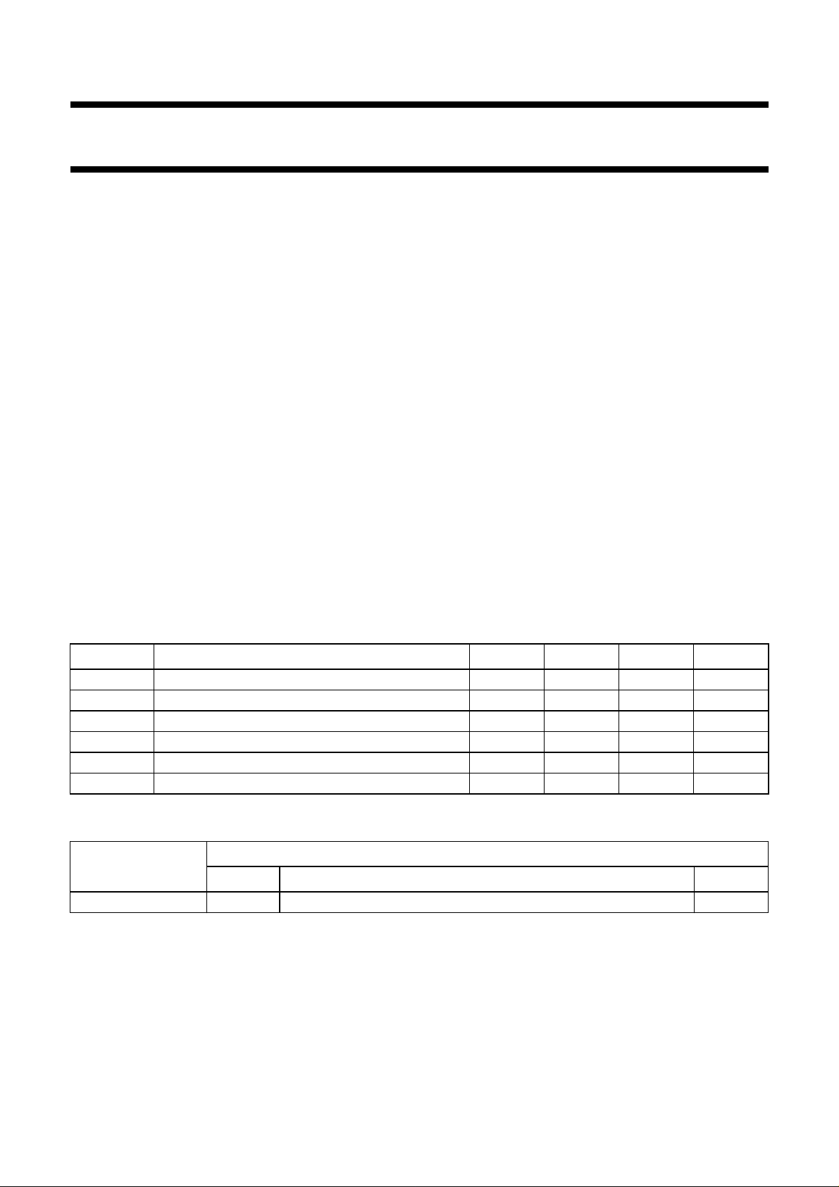
QUICK REFERENCE DATA
SYMBOL PARAMETER MIN. TYP. MAX. UNIT
V
P
I
P
I
P(PD)
f
in
V
in(M)
T
amb
supply voltage 4.5 5.0 5.5 V
supply current −−6.7 mA
supply current in power-down mode −−250 µA
operating input frequency −−15 MHz
dynamic logarithmic input voltage (peak value) 0.06 − 300 mV
operating ambient temperature −20 − +75 °C
ORDERING INFORMATION
PACKAGE
TYPE NUMBER
NAME DESCRIPTION VERSION
TDA8780M SSOP20 plastic shrink small outline package; 20 leads; body width 4.4 mm SOT266-1
1995 Jul 25 2
Page 3
Philips Semiconductors Product specification
True logarithmic amplifier TDA8780M
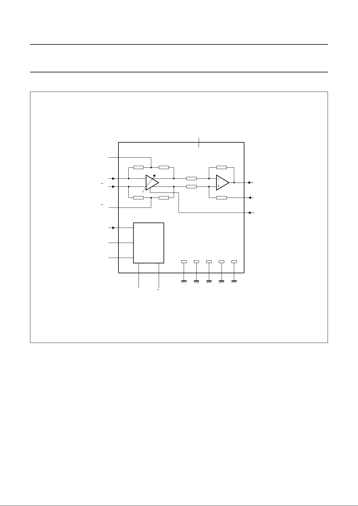
BLOCK DIAGRAM
book, full pagewidth
C
C
C
V
V
C
CE
DEC1
DEC2
V
P
11
6
lf
in
in
lf
100 k
1
20
100 k
15
16
3
CONTROL
18
R
100 k
Ω
Ω
100 k
Ω
20 k
Ω
20 k
Ω
Ω
20 k
20 k
Ω
13
8
Ω
17
TDA8780M
45 19
R
g
GND1 GND2 GND3 GND4 GND5
g
141072
V
out
V
ref
TEST
MBE161
Fig.1 Block diagram.
1995 Jul 25 3
Page 4
Philips Semiconductors Product specification
True logarithmic amplifier TDA8780M
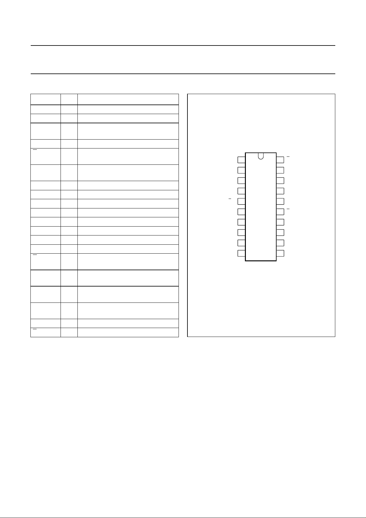
PINNING
SYMBOL PIN DESCRIPTION
V
in
GND1 2 ground 1
C
DEC1
R
g
R
g
C
lf
GND2 7 ground 2
V
ref
n.c. 9 not connected
GND3 10 ground 3 (main ground)
V
P
n.c. 12 not connected
V
out
GND4 14 ground 4
C
lf
CE 16 TTL-level-compatible circuit enable
TEST 17 test input; connected to ground in
C
DEC2
GND5 19 ground 5
V
in
1 signal voltage input
3 control circuit first decoupling and
optional start-up capacitor connection
4 small-signal gain-setting resistor
5 small-signal complementary
gain-setting resistor
6 low-frequency cut-off point setting
capacitor
8 external reference voltage input
11 power supply
13 true logarithmic voltage output
15 complementary low-frequency cut-off
point setting capacitor
input (active HIGH)
normal operation
18 control circuit second decoupling and
optional start-up capacitor
20 complementary signal voltage input
handbook, halfpage
V
1
in
GND1
2
C
3
DEC1
R
4
g
R
5
g
C
GND2
V
ref
n.c. n.c.
GND3
TDA8780M
6
lf
7
8
9
10
MBE160
Fig.2 Pin configuration.
V
20
in
GND5
19
C
18
DEC2
17
TEST
CE
16
C
15
lf
14
GND4
V
13
out
12
V
P
11
1995 Jul 25 4
Page 5

Philips Semiconductors Product specification
True logarithmic amplifier TDA8780M
FUNCTIONAL DESCRIPTION
A true logarithmic amplifier can be realized from a cascade
of similar stages each stage consisting of a pair of
amplifiers whose inputs and outputs are connected in
parallel. One of these amplifiers can be formed by an
undegenerated long-tailed pair which provides high gain
but limited linear input signal-handling capability. The
other amplifier can be formed by a degenerated long-tailed
pair which provides a gain of unity and a much larger linear
input signal-handling capability.
The overall cascade amplifies very small input signals but,
once these reach the level at which the undegenerated
long-tailed pair in the last stage is at the limit of its linear
signal-handling capability, the output voltage becomes
logarithmically dependent on the input signal level. This
behaviour continues until the input signal reaches the level
at which undegenerated long-tailed pair in the first stage is
at the limit of its linear input signal-handling capability. The
transfer characteristic beyond this point then depends on
the exact configuration of the degenerated long-tailed pair
in the first stage.
Five stages are used in the TDA8780M to provide a 72 dB
true logarithmic dynamic range. The DC bias current in the
undegenerated long-tailed pair in the first stage is made
externally adjustable, using an off-chip resistor, to provide
a small-signal gain adjustment facility. The small signal
gain defined by this resistor is valid when the IC is
operating in the “linear” mode, for input signals typically
less than 60 µV.
A high-level limiter is inserted between the first and second
stages to provide a constant limiting output voltage which
is essentially independent of the value of the gain setting
resistor. These stages can be driven by single-ended or
differential inputs. The DC operating point is set by overall
on-chip feedback decoupled by two off-chip capacitors
which define the low-frequency cut-off point. The
performance is stabilized against temperature and DC
power supply variations. The input to the true logarithmic
amplifier is protected against damage due to excessive
differential input signals by diodes.
The differential output from the true logarithmic amplifier is
converted internally to a single-ended output by an on-chip
operational amplifier arrangement in which the DC output
level is set by an externally-supplied reference voltage.
The output is capable of driving loads down to 10 kΩ. The
limiting output voltage and the output drive capability have
been chosen to facilitate interfacing to analog-to-digital
converters. A major part of the DC power supply current
consumption of the device is associated with provision of
this output drive capability. The DC power supply
consumption is significantly less when the device is driving
smaller loads.
A power-down facility allows the circuit to be disabled from
a TTL-level compatible control input.
1995 Jul 25 5
Page 6

Philips Semiconductors Product specification
True logarithmic amplifier TDA8780M
LIMITING VALUES
In accordance with the Absolute Maximum Rating System (IEC 134).
SYMBOL PARAMETER MIN. MAX. UNIT
V
P
V
i
T
amb
T
stg
HANDLING
Inputs and outputs are protected against electrostatic discharge in normal handling. However, to be totally safe, it is
desirable to take normal precautions appropriate to handling MOS devices.
supply voltage −0.3 +6.0 V
input voltage all other pins referenced to ground −0.3 VP+ 0.3 V
operating ambient temperature −20 +75 °C
IC storage temperature −55 +150 °C
ESD in accordance with
“MIL STD 883C” -“Method 3015”
.
CHARACTERISTICS
V
=5V; T
P
=25°C; V
amb
= 2.5 V; Vinat fin= 10.7 MHz; Rg= 3.3 kΩ; output not loaded; unless otherwise specified.
ref
Signal values expressed as peak voltages mV (peak), µV (peak) or dBm (50 Ω).
SYMBOL PARAMETER CONDITIONS MIN. TYP. MAX. UNIT
Supply
V
P
I
P
I
P(PD)
t
sw
supply voltage 4.5 5.0 5.5 V
supply current VP= 5.5 V; Vin=1V − 5.4 6.7 mA
= 5.0 V; Vin=1V − 4.9 6.2 mA
V
P
supply current in power-down output not loaded − 40 200 µA
R
=10kΩ−100 250 µA
L
switching time see Fig.6 − 70 −µs
Reference input (pin 8)
V
ref
R
ref
external reference voltage input 2.0 2.5 VP− 2.0 V
external reference resistance input − 40 − kΩ
Inputs (pins 1 and 20)
f
in
R
diff
input operating frequency note 1 1.0 10.7 15 MHz
differential small-signal input
Vin=10mV − 10 − kΩ
resistance
C
diff
V
in(min)
differential input capacitance − 2 − pF
input voltage level at start of
− 60 −µV
logarithmic characteristic
V
in(top)
input voltage level at top end of
− 300 − mV
logarithmic characteristic
V
in(max)
maximum input signal voltage input protection diodes not
− 1 − V
conducting
∆V
in
input voltage level spread across
over whole T
and VP range −±2.5 − dB
amb
logarithmic range
1995 Jul 25 6
Page 7

Philips Semiconductors Product specification
True logarithmic amplifier TDA8780M
SYMBOL PARAMETER CONDITIONS MIN. TYP. MAX. UNIT
Output (pin 13)
V
os
V
out
DC offset voltage (V
output voltage level across
logarithmic range
V
out(lim)
limiting output voltage Vin= 1 V (+13.0 dBm) 750 950 1050 mV
∆ϕ spread in output phase transfer
characteristic across logarithmic
range
f
lf
G
flat
R
13
low frequency cut-off point (3 dB) see Fig.6 −−0.1 MHz
gain flatness at 1 to 15 MHz Vin=10mV − 0.5 1.5 dB
output resistance − 150 −Ω
Logic input (pin 16)
V
IL
V
IH
I
LI
LOW level input voltage 0 − 0.8 V
HIGH level input voltage 2 − V
input leakage current VIL=0toV
Note
1. With some changes in application the lower input frequency limit can be lowered.
out
to V
) no input signal −60 +40 +140 mV
ref
Vin=60µV (−71.4 dBm) 45 80 115 mV
V
= 400 µV (−54.9 dBm) 200 245 290 mV
in
V
= 3 mV (−37.4 dBm) 365 440 495 mV
in
= 25 mV (−19.0 dBm) 530 610 690 mV
V
in
V
= 200 mV (−1.0 dBm) 680 780 880 mV
in
V
= 300 mV (+2.6 dBm) 710 820 930 mV
in
R
= 0; Vin= 3 mV; see Fig.3 − 530 − mV
g
R
= ∞; Vin= 3 mV; see Fig.3 − 360 − mV
g
− 15 −
P
−1 − +1 µA
P
V
1995 Jul 25 7
Page 8

Philips Semiconductors Product specification
True logarithmic amplifier TDA8780M
1000
handbook, halfpage
V
out
(mV)
800
600
400
200
0
80 20
VCC= 5 V; V
60 40 20 0
= 2.5 V; fin= 10 MHz; T
ref
Fig.3 Output voltage dependence on Rg.
MLD209
R = 0
g
R = 3.3 kΩ
g
∞
R =
g
V (dBm, 50 Ω)
in
=25°C.
amb
1000
handbook, halfpage
V
out
(mV)
800
600
400
200
0
80 20
60 40 20 0
Fig.4 Typical transfer characteristics.
MGC118
V (dBm, 50 Ω)
in
Rg =
MGC666
∞
100
handbook, halfpage
V
out
(mV)
75
50
25
0
0 100
Rg = 0 Rg = 3.3 kΩ
50
Vin (µV)
Fig.5 Typical small signal gain.
1995 Jul 25 8
Page 9

Philips Semiconductors Product specification
True logarithmic amplifier TDA8780M
APPLICATION INFORMATION
The circuit is typically connected as shown in Fig.6. The
single-ended 10.7 MHz input IF signal is applied
(arbitrarily) to one of the two input pins via a ceramic filter.
These inputs should not be DC coupled as this will disable
the on-chip feedback which sets the DC operating point of
the true logarithmic amplifier. The relatively high
impedance of these inputs facilitates correct termination of
the ceramic filter by an off-chip resistor.
IF input
IF filter 10.7 MHz
330 Ω
3.3 kΩ
100 pF
100 pF
56 pF
C
V
GND1
DEC1
R
R
C
in
1
2
3
g
4
g
5
lf
6
handbook, full pagewidth
The low-frequency cut-off point is determined by the value
of capacitors connected to pins 6 and 15 which decouple
the overall DC feedback and the value of the input coupling
capacitors. The output is coupled to an analog-to-digital
converter thus the value of the voltage fed to the reference
voltage input is not critical. It could be useful in other
applications, where the output may be DC coupled to an
alternative analog-to-digital converter, to derive this
reference voltage from the centre of the input resistor
chain of the analog-to-digital converter.
100 pF
V
in
20
GND5
19
C
DEC2
18
17
16
TDA8780M
15
TEST
CE
C
lf
33 pF
56 pF
circuit
enable
input
GND2 GND4
7
V
ref
2.5 V
8
n.c. n.c.
9
GND3
10
Fig.6 Typical application diagram.
1995 Jul 25 9
14
13
12
11
MGC117
V
out
V
P
output to
ADC
5 V
47 nF2.2 nF
Page 10

Philips Semiconductors Product specification
True logarithmic amplifier TDA8780M
PACKAGE OUTLINE
SSOP20: plastic shrink small outline package; 20 leads; body width 4.4 mm
D
c
y
Z
20
pin 1 index
11
A
2
A
1
110
w M
b
e
p
E
H
E
detail X
SOT266-1
A
X
v M
A
Q
(A )
L
p
L
A
3
θ
0 2.5 5 mm
scale
DIMENSIONS (mm are the original dimensions)
UNIT A1A2A
mm
Note
1. Plastic or metal protrusions of 0.20 mm maximum per side are not included.
A
max.
1.5
OUTLINE
VERSION
SOT266-1
0.1501.4
1.2
b
3
p
0.32
0.20
0.20
0.13
0.25
IEC JEDEC EIAJ
(1)E(1)
cD
6.6
6.4
REFERENCES
4.5
0.65 1.0 0.2
4.3
1995 Jul 25 10
eHELLpQZywv θ
6.6
6.2
0.75
0.45
0.65
0.45
PROJECTION
0.13 0.1
EUROPEAN
(1)
0.48
0.18
ISSUE DATE
90-04-05
95-02-25
o
10
o
0
Page 11

Philips Semiconductors Product specification
True logarithmic amplifier TDA8780M
SOLDERING
Introduction
There is no soldering method that is ideal for all IC
packages. Wave soldering is often preferred when
through-hole and surface mounted components are mixed
on one printed-circuit board. However, wave soldering is
not always suitable for surface mounted ICs, or for
printed-circuits with high population densities. In these
situations reflow soldering is often used.
This text gives a very brief insight to a complex technology.
A more in-depth account of soldering ICs can be found in
our
“IC Package Databook”
Reflow soldering
Reflow soldering techniques are suitable for all SO
packages.
Reflow soldering requires solder paste (a suspension of
fine solder particles, flux and binding agent) to be applied
to the printed-circuit board by screen printing, stencilling or
pressure-syringe dispensing before package placement.
Several techniques exist for reflowing; for example,
thermal conduction by heated belt. Dwell times vary
between 50 and 300 seconds depending on heating
method. Typical reflow temperatures range from
215 to 250 °C.
(order code 9398 652 90011).
During placement and before soldering, the package must
be fixed with a droplet of adhesive. The adhesive can be
applied by screen printing, pin transfer or syringe
dispensing. The package can be soldered after the
adhesive is cured.
Maximum permissible solder temperature is 260 °C, and
maximum duration of package immersion in solder is
10 seconds, if cooled to less than 150 °C within
6 seconds. Typical dwell time is 4 seconds at 250 °C.
A mildly-activated flux will eliminate the need for removal
of corrosive residues in most applications.
Repairing soldered joints
Fix the component by first soldering two diagonallyopposite end leads. Use only a low voltage soldering iron
(less than 24 V) applied to the flat part of the lead. Contact
time must be limited to 10 seconds at up to 300 °C. When
using a dedicated tool, all other leads can be soldered in
one operation within 2 to 5 seconds between
270 and 320 °C.
Preheating is necessary to dry the paste and evaporate
the binding agent. Preheating duration: 45 minutes at
45 °C.
Wave soldering
Wave soldering techniques can be used for all SO
packages if the following conditions are observed:
• A double-wave (a turbulent wave with high upward
pressure followed by a smooth laminar wave) soldering
technique should be used.
• The longitudinal axis of the package footprint must be
parallel to the solder flow.
• The package footprint must incorporate solder thieves at
the downstream end.
1995 Jul 25 11
Page 12

Philips Semiconductors Product specification
True logarithmic amplifier TDA8780M
DEFINITIONS
Data sheet status
Objective specification This data sheet contains target or goal specifications for product development.
Preliminary specification This data sheet contains preliminary data; supplementary data may be published later.
Product specification This data sheet contains final product specifications.
Limiting values
Limiting values given are in accordance with the Absolute Maximum Rating System (IEC 134). Stress above one or
more of the limiting values may cause permanent damage to the device. These are stress ratings only and operation
of the device at these or at any other conditions above those given in the Characteristics sections of the specification
is not implied. Exposure to limiting values for extended periods may affect device reliability.
Application information
Where application information is given, it is advisory and does not form part of the specification.
LIFE SUPPORT APPLICATIONS
These products are not designed for use in life support appliances, devices, or systems where malfunction of these
products can reasonably be expected to result in personal injury. Philips customers using or selling these products for
use in such applications do so at their own risk and agree to fully indemnify Philips for any damages resulting from such
improper use or sale.
1995 Jul 25 12
Page 13

Philips Semiconductors Product specification
True logarithmic amplifier TDA8780M
NOTES
1995 Jul 25 13
Page 14

Philips Semiconductors Product specification
True logarithmic amplifier TDA8780M
NOTES
1995 Jul 25 14
Page 15

Philips Semiconductors Product specification
True logarithmic amplifier TDA8780M
NOTES
1995 Jul 25 15
Page 16

Philips Semiconductors – a worldwide company
Argentina: IEROD, Av. Juramento 1992 - 14.b, (1428)
BUENOS AIRES, Tel. (541)786 7633, Fax. (541)786 9367
Australia: 34 Waterloo Road, NORTH RYDE, NSW 2113,
Tel. (02)805 4455, Fax. (02)805 4466
Austria: Triester Str. 64, A-1101 WIEN, P.O. Box 213,
Tel. (01)60 101-1236, Fax. (01)60 101-1211
Belgium: Postbus 90050, 5600 PB EINDHOVEN, The Netherlands,
Tel. (31)40 783 749, Fax. (31)40 788 399
Brazil: Rua do Rocio 220 - 5
CEP: 04552-903-SÃO PAULO-SP, Brazil.
P.O. Box 7383 (01064-970),
Tel. (011)821-2333, Fax. (011)829-1849
Canada: PHILIPS SEMICONDUCTORS/COMPONENTS:
Tel. (800) 234-7381, Fax. (708) 296-8556
Chile: Av. Santa Maria 0760, SANTIAGO,
Tel. (02)773 816, Fax. (02)777 6730
China/Hong Kong: 501 Hong Kong Industrial Technology Centre,
72 Tat Chee Avenue, Kowloon Tong, HONG KONG,
Tel. (852)2319 7888, Fax. (852)2319 7700
Colombia: IPRELENSO LTDA, Carrera 21 No. 56-17,
77621 BOGOTA, Tel. (571)249 7624/(571)217 4609,
Fax. (571)217 4549
Denmark: Prags Boulevard 80, PB 1919, DK-2300
COPENHAGEN S, Tel. (032)88 2636, Fax. (031)57 1949
Finland: Sinikalliontie 3, FIN-02630 ESPOO,
Tel. (358)0-615 800, Fax. (358)0-61580 920
France: 4 Rue du Port-aux-Vins, BP317,
92156 SURESNES Cedex,
Tel. (01)4099 6161, Fax. (01)4099 6427
Germany: P.O. Box 10 63 23, 20043 HAMBURG,
Tel. (040)3296-0, Fax. (040)3296 213.
Greece: No. 15, 25th March Street, GR 17778 TAVROS,
Tel. (01)4894 339/4894 911, Fax. (01)4814 240
India: Philips INDIA Ltd, Shivsagar Estate, A Block,
Dr. Annie Besant Rd. Worli, Bombay 400 018
Tel. (022)4938 541, Fax. (022)4938 722
Indonesia: Philips House, Jalan H.R. Rasuna Said Kav. 3-4,
P.O. Box 4252, JAKARTA 12950,
Tel. (021)5201 122, Fax. (021)5205 189
Ireland: Newstead, Clonskeagh, DUBLIN 14,
Tel. (01)7640 000, Fax. (01)7640 200
Italy: PHILIPS SEMICONDUCTORS S.r.l.,
Piazza IV Novembre 3, 20124 MILANO,
Tel. (0039)2 6752 2531, Fax. (0039)2 6752 2557
Japan: Philips Bldg13-37, Kohnan 2-chome, Minato-ku, TOKYO 108,
Tel. (03)3740 5130, Fax. (03)3740 5077
Korea: Philips House, 260-199 Itaewon-dong,
Yongsan-ku, SEOUL, Tel. (02)709-1412, Fax. (02)709-1415
Malaysia: No. 76 Jalan Universiti, 46200 PETALING JAYA,
SELANGOR, Tel. (03)750 5214, Fax. (03)757 4880
Mexico: 5900 Gateway East, Suite 200, EL PASO, TX 79905,
Tel. 9-5(800)234-7381, Fax. (708)296-8556
th
floor, Suite 51,
Netherlands: Postbus 90050, 5600 PB EINDHOVEN, Bldg. VB,
Tel. (040)783749, Fax. (040)788399
(From 10-10-1995: Tel. (040)2783749, Fax. (040)2788399)
New Zealand: 2 Wagener Place, C.P.O. Box 1041, AUCKLAND,
Tel. (09)849-4160, Fax. (09)849-7811
Norway: Box 1, Manglerud 0612, OSLO,
Tel. (022)74 8000, Fax. (022)74 8341
Pakistan: Philips Electrical Industries of Pakistan Ltd.,
Exchange Bldg. ST-2/A, Block 9, KDA Scheme 5, Clifton,
KARACHI 75600, Tel. (021)587 4641-49,
Fax. (021)577035/5874546
Philippines: PHILIPS SEMICONDUCTORS PHILIPPINES Inc,
106 Valero St. Salcedo Village, P.O. Box 2108 MCC, MAKATI,
Metro MANILA, Tel. (02)810 0161, Fax. (02)817 3474
Portugal: PHILIPS PORTUGUESA, S.A.,
Rua dr. António Loureiro Borges 5, Arquiparque - Miraflores,
Apartado 300, 2795 LINDA-A-VELHA,
Tel. (01)4163160/4163333, Fax. (01)4163174/4163366
Singapore: Lorong 1, Toa Payoh, SINGAPORE 1231,
Tel. (65)350 2000, Fax. (65)251 6500
South Africa: S.A. PHILIPS Pty Ltd.,
195-215 Main Road Martindale, 2092 JOHANNESBURG,
P.O. Box 7430, Johannesburg 2000,
Tel. (011)470-5911, Fax. (011)470-5494.
Spain: Balmes 22, 08007 BARCELONA,
Tel. (03)301 6312, Fax. (03)301 42 43
Sweden: Kottbygatan 7, Akalla. S-164 85 STOCKHOLM,
Tel. (0)8-632 2000, Fax. (0)8-632 2745
Switzerland: Allmendstrasse 140, CH-8027 ZÜRICH,
Tel. (01)488 2211, Fax. (01)481 77 30
Taiwan: PHILIPS TAIWAN Ltd., 23-30F, 66, Chung Hsiao West
Road, Sec. 1. Taipeh, Taiwan ROC, P.O. Box 22978,
TAIPEI 100, Tel. (02)388 7666, Fax. (02)382 4382
Thailand: PHILIPS ELECTRONICS (THAILAND) Ltd.,
209/2 Sanpavuth-Bangna Road Prakanong,
Bangkok 10260, THAILAND,
Tel. (662)398-0141, Fax. (662)398-3319
Turkey:Talatpasa Cad. No. 5, 80640 GÜLTEPE/ISTANBUL,
Tel. (0212)279 27 70, Fax. (0212)282 67 07
United Kingdom: Philips Semiconductors LTD.,
276 Bath Road, Hayes, MIDDLESEX UB3 5BX,
Tel. (0181)730-5000, Fax. (0181)754-8421
United States:811 East Arques Avenue, SUNNYVALE,
CA 94088-3409, Tel. (800)234-7381, Fax. (708)296-8556
Uruguay: Coronel Mora 433, MONTEVIDEO,
Tel. (02)70-4044, Fax. (02)92 0601
Internet: http://www.semiconductors.philips.com/ps/
For all other countries apply to: Philips Semiconductors,
International Marketing and Sales, Building BE-p,
P.O. Box 218, 5600 MD EINDHOVEN, The Netherlands,
Telex 35000 phtcnl, Fax. +31-40-724825 (from 10-10-1995: +31-40-2724825)
SCD41 © Philips Electronics N.V. 1995
All rights are reserved. Reproduction in whole or in part is prohibited without the
prior written consent of the copyright owner.
The information presented in this document does not form part of any quotation
or contract, is believed to be accurate and reliable and may be changed without
notice. No liability will be accepted by the publisher for any consequence of its
use. Publication thereof does not convey nor imply any license under patent- or
other industrial or intellectual property rights.
Printed in The Netherlands
413061/1500/02/pp16 Date of release: 1995 Jul 25
Document order number: 9397 750 00234
 Loading...