

Page 1

INTEGRATED CIRCUITS
DATA SH EET
TDA8766
10-bit high-speed 3.0 to 5.25 V
analog-to-digital converter
Product specification
Supersedes data of 2000 May 25
File under Integrated Circuits, IC02
2001 Apr 19
Page 2

Philips Semiconductors Product specification
10-bit high-speed 3.0 to 5.25 V
analog-to-digital converter
FEATURES
• 10-bit resolution
• 3.0 to 5.25 V operation
• Sampling rate up to 20 MHz
• DC sampling allowed
• High signal-to-noise ratio over a large analog input
frequency range(9.3 effective bits at 1.0 MHz; full-scale
input at f
• In-Range (IR) CMOS output
• CMOS/TTL compatible digital inputs and outputs
• External reference voltage regulator
• Power dissipation only 53 mW (typical value)
• Low analog input capacitance, no buffer amplifier
required
• Standby mode
• No sample-and-hold circuit required.
= 20 MHz)
clk
TDA8766
APPLICATIONS
High-speed analog-to-digital conversion for:
• Video data digitizing
• Camera
• Camcorder
• Radio communication.
GENERAL DESCRIPTION
The TDA8766 is a 10-bit high-speed Analog-to-Digital
Converter (ADC) for professional video and other
applications. It converts with 3.0 to 5.25 V operation the
analoginput signalinto10-bit binary-codeddigitalwords at
a maximumsampling rateof 20 MHz. Alldigital inputs and
outputs are CMOS compatible. A standby mode allows
reduction ofthe devicepower consumptiondown to 4 mW.
QUICK REFERENCE DATA
SYMBOL PARAMETER CONDITIONS MIN. TYP. MAX. UNIT
V
V
V
V
I
DDA
I
DDD
I
DDO
DDA
DDD1
DDD2
DDO
analog supply voltage 3.0 3.3 5.25 V
digital supply voltage 1 3.0 3.3 5.25 V
digital supply voltage 2 3.0 3.3 5.25 V
output stages supply voltage 3.0 3.3 5.25 V
analog supply current − 7.5 10 mA
digital supply current − 7.5 10 mA
output stages supply current f
= 20 MHz; CL= 20 pF; ramp
clk
− 12mA
input
INL integral non-linearity f
DNL differential non-linearity f
f
clk(max)
P
tot
maximum clock frequency 20 −−MHz
total power dissipation V
= 20 MHz; ramp input −±1±2 LSB
clk
= 20 MHz; ramp input −±0.25 ±0.7 LSB
clk
DDA=VDDD=VDDO
= 3.3 V − 53 73 mW
ORDERING INFORMATION
TYPE
NUMBER
NAME DESCRIPTION VERSION
PACKAGE
TDA8766G LQFP32 plastic low profile quad flat package; 32 leads; body 5 × 5 × 1.4 mm SOT401-1
2001 Apr 19 2
Page 3
Philips Semiconductors Product specification
10-bit high-speed 3.0 to 5.25 V
analog-to-digital converter
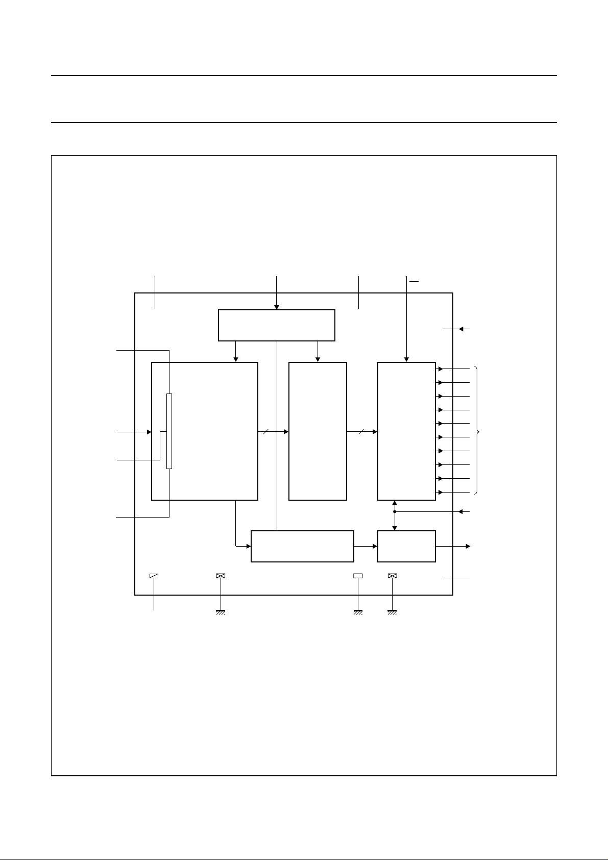
BLOCK DIAGRAM
handbook, full pagewidth
analog
voltage input
V
RT
V
V
RM
V
DDA
7
15
R
LAD
I
14
11
ANALOG -TO - DIGITAL
CONVERTER
CLK
5
CLOCK DRIVER
LATCHES
V
DDD2
18
TDA8766
OE
16
CMOS
OUTPUTS
6
1
D9
D8
31
D7
30
D6
29
D5
28
27 D4
26
D3
25
D2
23 D1
22
D0
TDA8766
STDBY
MSB
data outputs
LSB
V
10
RB
IN-RANGE LATCH
9
V
analog
ground
SSA
19
V
digital
ground 2
SSD2
Fig.1 Block diagram.
2001 Apr 19 3
V
SSOVSSD1
output
ground
CMOS
OUTPUT
321
digital
ground 1
20
MLC853
V
DDO
2
4
IR output
V
DDD1
Page 4
Philips Semiconductors Product specification
10-bit high-speed 3.0 to 5.25 V
analog-to-digital converter
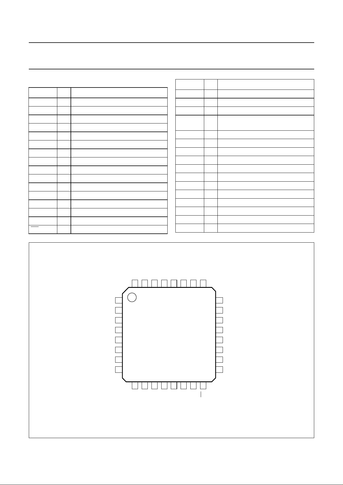
PINNING
SYMBOL PIN DESCRIPTION
D9 1 data output; bit 9 (MSB)
IR 2 in-range data output
V
SSD1
V
DDD1
CLK 5 clock input
STDBY 6 standby mode input
V
DDA
n.c. 8 not connected
V
SSA
V
RB
V
RM
n.c. 12 not connected
n.c. 13 not connected
V
I
V
RT
OE 16 output enable input (active LOW)
3 digital ground 1
4 digital supply voltage 1 (3.0 to 5.25 V)
7 analog supply voltage (3.0 to 5.25 V)
9 analog ground
10 reference voltage BOTTOM input
11 reference voltage MIDDLE input
14 analog voltage input
15 reference voltage TOP input
TDA8766
SYMBOL PIN DESCRIPTION
n.c. 17 not connected
V
DDD2
V
SSD2
V
DDO
V
SSO
D0 22 data output; bit 0 (LSB)
D1 23 data output; bit 1
n.c. 24 not connected
D2 25 data output; bit 2
D3 26 data output; bit 3
D4 27 data output; bit 4
D5 28 data output; bit 5
D6 29 data output; bit 6
D7 30 data output; bit 7
D8 31 data output; bit 8
n.c. 32 not connected
18 digital supply voltage 2 (3.0 to 5.25 V)
19 digital ground 2
20 positive supply voltage for
output stage (3.0 to 5.25 V)
21 output stage ground
handbook, full pagewidth
D9
V
SSD1
V
DDD1
CLK
STDBY
V
DDA
n.c.
n.c.
D8
D7
D6
D5
D4
D3
D2
32
31
30
29
28
27
26
25
1
2
IR
3
4
TDA8766
5
6
7
8
9
10
11
12
13
14
15
16
RT
OE
V
SSA
V
I
RB
RM
V
n.c.
V
n.c.
V
24
23
22
21
20
19
18
17
MLC854
n.c.
D1
D0
V
SSO
V
DDO
V
SSD2
V
DDD2
n.c.
Fig.2 Pin configuration.
2001 Apr 19 4
Page 5
Philips Semiconductors Product specification
10-bit high-speed 3.0 to 5.25 V
TDA8766
analog-to-digital converter
LIMITING VALUES
In accordance with the Absolute Maximum Rating System (IEC 60134).
SYMBOL PARAMETER CONDITIONS MIN. MAX. UNIT
V
V
V
∆V
V
V
I
O
T
T
T
DDA
DDD
DDO
DD
I
i(p-p)
stg
amb
j
analog supply voltage note 1 −0.3 +7.0 V
digital supply voltage note 1 −0.3 +7.0 V
output stages supply voltage note 1 −0.3 +7.0 V
supply voltage difference
V
− V
V
V
DDA
DDD
DDA
− V
− V
DDD
DDO
DDO
input voltage referenced to V
AC input voltage for switching
referenced to V
SSA
SSD
−1.0 +4.0 V
−1.0 +4.0 V
−1.0 +4.0 V
−0.3 +7.0 V
− V
DDD
(peak-to-peak value)
output current − 10 mA
storage temperature −55 +150 °C
ambient temperature −20 +75 °C
junction temperature − 150 °C
V
Note
1. The supply voltages V
DDA
, V
DDD
and V
may have any value between −0.3 and +7.0 V provided that the supply
DDO
voltage differences ∆VDD are respected.
HANDLING
Inputs and outputs are protected against electrostatic discharges in normal handling. However, to be totally safe, it is
desirable to take normal precautions appropriate to handling integrated circuits.
THERMAL CHARACTERISTICS
SYMBOL PARAMETER CONDITIONS VALUE UNIT
R
th(jj-a)
thermal resistance from junction to ambient in free air 90 K/W
2001 Apr 19 5
Page 6
Philips Semiconductors Product specification
10-bit high-speed 3.0 to 5.25 V
TDA8766
analog-to-digital converter
CHARACTERISTICS
V
DDA=V7
short-circuited together; V
otherwise specified.
SYMBOL PARAMETER CONDITIONS MIN. TYP. MAX. UNIT
Supplies
V
DDA
V
DDD1
V
DDD2
V
DDO
∆V
I
DDA
I
DDD
I
DDO
P
tot
Inputs
DD
to V9= 3.3 V; V
DDD=V4
i(p-p)
to V3=V18to V19= 3.3 V; V
= 1.83 V;CL= 20 pF; T
DDO=V20
= 0 to 70 °C; typicalvalues measured at T
amb
to V21= 3.3 V; V
SSA,VSSD
and V
SSO
=25°C; unless
amb
analog supply voltage 3.0 3.3 5.25 V
digital supply voltage 1 3.0 3.3 5.25 V
digital supply voltage 2 3.0 3.3 5.25 V
output stages supply voltage 3.0 3.3 5.25 V
voltage difference
V
V
V
DDA
DDA
DDD
− V
− V
− V
DDD
DDO
DDO
−0.2 − +0.2 V
−0.2 − +2.25 V
−0.2 − +2.25 V
analog supply current − 7.5 10 mA
digital supply current − 7.5 10 mA
output stages supply current f
= 20 MHz;
clk
− 12mA
ramp input; CL=20pF
total power dissipation operating; VDD= 3.3 V − 53 73 mW
standby mode − 4 − mW
C
LOCK INPUT CLK (REFERENCED TO V
V
IL
V
IH
I
IL
I
IH
Z
i
C
i
LOW-level input voltage 0 − 0.3V
HIGH-level input voltage V
LOW-level input current V
HIGH-level input current V
input impedance f
input capacitance f
SSD
); note 1
INPUTS OE AND STDBY (REFERENCED TO V
V
IL
V
IH
I
IL
I
IH
ANALOG INPUT VI(REFERENCED TO V
I
IL
I
IH
Z
i
C
i
LOW-level input voltage 0 − 0.3V
HIGH-level input voltage V
LOW-level input current VIL= 0.3 V
HIGH-level input current VIH= 0.7 V
)
SSA
LOW-level input current VI=V
HIGH-level input current VI=V
input impedance fi= 1 MHz − 5 − kΩ
input capacitance fi= 1 MHz − 8 − pF
≤ 3.6 V 0.6V
DDD
V
= 3.3 V 0.7V
DDD
= 0.3V
CLK
= 0.7V
CLK
= 20 MHz − 4 − kΩ
clk
= 20 MHz − 3 − pF
clk
); see Tables 1 and 2
SSD
≤ 3.6 V 0.6V
DDD
V
= 3.3 V 0.7V
DDD
RB
RT
DDD
DDD
DDD
DDD
V
DDD
DDD
DDD
− V
− V
DDD
DDD
V
V
−10+1µA
−−5µA
V
DDD
DDD
DDD
− V
− V
DDD
DDD
V
V
−1 −−µA
−−1µA
− 0 −µA
− 35 −µA
2001 Apr 19 6
Page 7
Philips Semiconductors Product specification
10-bit high-speed 3.0 to 5.25 V
TDA8766
analog-to-digital converter
SYMBOL PARAMETER CONDITIONS MIN. TYP. MAX. UNIT
Reference voltages for resistor ladder; see Table 3
V
RB
V
RT
V
diff(ref)
I
ref
R
LAD
TC
RLAD
V
offset(B)
V
offset(T)
V
I(p-p)
Outputs
DIGITAL OUTPUTS D9 TO D0 AND IR (REFERENCED TO V
V
OL
V
OH
I
OZ
Switching characteristics
reference voltage BOTTOM 1.1 1.2 − V
reference voltage TOP 3.0 3.3 V
differential reference voltage
VRT− V
RB
1.9 2.1 3.0 V
DDA
V
reference current − 7.2 − mA
ladder resistance − 290 −Ω
temperature coefficient of ladder
resistance
− 539 − mΩ/K
− 1860 − ppm
offset voltage BOTTOM note 2 − 135 − mV
offset voltage TOP note 2 − 135 − mV
analog input voltage
note 3 1.66 1.83 2.35 V
(peak-to-peak value)
)
SSD
LOW-level output voltage IO=1mA 0 − 0.5 V
HIGH-level output voltage IO= −1mA V
output current in 3-state mode 0.5 V < VO<V
DDO
− 0.5 − V
DDO
DDO
V
−20 −+20 µA
CLOCK INPUT CLK; see Fig.4; note 1
f
clk(max)
t
CPH
t
CPL
Analog signal processing (f
L
INEARITY
maximum clock frequency 20 −−MHz
clock pulse width HIGH 15 −−ns
clock pulse width LOW 15 −−ns
= 20 MHz)
clk
INL integral non-linearity ramp input; see Fig.6 −±1±2 LSB
DNL differential non-linearity ramp input; see Fig.7 −±0.25 ±0.7 LSB
I
NPUT SET RESPONSE; see Fig.8; note 4
t
STLH
analog input settling time
full-scale square wave − 46ns
LOW-to-HIGH
t
STHL
analog input settling time
full-scale square wave − 46ns
HIGH-to-LOW
HARMONICS; see Fig.9; note 5
THD total harmonic distortion f
= 1 MHz −−63 − dB
i
SIGNAL-TO-NOISE RATIO; see Fig.9; note 5
S/N signal-to-noise ratio (full-scale) without harmonics;
= 1 MHz
f
i
− 60 − dB
2001 Apr 19 7
Page 8

Philips Semiconductors Product specification
10-bit high-speed 3.0 to 5.25 V
TDA8766
analog-to-digital converter
SYMBOL PARAMETER CONDITIONS MIN. TYP. MAX. UNIT
E
FFECTIVE BITS; see Fig.9; note 5
EB effective bits f
Timing (f
t
ds
t
h
t
d
= 20 MHz; CL= 20 pF); see Fig.4; note 6
clk
sampling delay time −−5ns
output hold time 5 −−ns
output delay time V
3-state output delay times; see Fig.5
t
dZH
t
dZL
t
dHZ
t
dLZ
enable HIGH − 14 18 ns
enable LOW − 16 20 ns
disable HIGH − 16 20 ns
disable LOW − 14 18 ns
Standby mode output delay times
t
d(stb)LH
t
d(stb)HL
standby LOW-to-HIGH transition −−200 ns
start-up HIGH-to-LOW transition −−500 ns
Notes
1. In additionto agood layoutof thedigital andanalog ground,it isrecommended thatthe riseand falltimes ofthe clock
must not be less than 1 ns.
2. Analog input voltages producing code 0 up to and including 1023:
a) V
(offset voltage BOTTOM) is the difference between the analog input which produces data equal to 00
offset(B)
and the reference voltage BOTTOM (VRB) at T
b) V
(offset voltage TOP) is the difference between VRT(reference voltage TOP) and the analog input which
offset(T)
produces data outputs equal to 1023 at T
3. In orderto ensure theoptimum linearity performanceof such converterarchitecture, the lowerand upper extremities
of theconverter reference resistorladder (corresponding tooutput codes 0 and 1023 respectively) areconnected to
pins VRB and VRT via offset resistors ROB and ROT as shown in Fig.3.
= 300 kHz − 9.5 − bits
i
f
= 1 MHz − 9.3 − bits
i
f
= 3.58 MHz − 8.0 − bits
i
= 4.75 V 8 12 15 ns
DDO
V
= 3.15 V 8 17 20 ns
DDO
=25°C.
amb
=25°C.
amb
a) Thecurrentflowing intothe resistorladderis andthe full-scaleinput range atthe converter,
to cover code 0 to code 1023, is
V
I
RLIL×
I
L
VRTVRB–
=
------------------------------------------
++
R
OBRLROT
R
-----------------------------------------R
L
++
OBRLROT
–()0.871 V
V
RTVRB
–()×=×==
RTVRB
b) Since RL, ROBand ROT have similar behaviour with respect to process and temperature variation, the ratio
R
----------------------------------------R
L
++
OBRLROT
codes ata giveninput voltage depends mainly onthe differenceV
will be kept reasonably constant from device to device. Consequently variation of the output
− VRBand itsvariation withtemperature and
RT
supply voltage. When several ADCs are connected in parallel and fed with the same reference source, the
matching between each of them is then optimized.
4. The analoginput settlingtime isthe minimum time required forthe inputsignal tobe stabilized aftera sharpfull-scale
input change (square-wave signal) in order to sample the signal and obtain correct output data.
2001 Apr 19 8
Page 9

Philips Semiconductors Product specification
10-bit high-speed 3.0 to 5.25 V
TDA8766
analog-to-digital converter
5. Effective bits are obtained via a Fast Fourier Transform (FFT) treatment taking 8k acquisition points per equivalent
fundamental period. The calculation takes into account all harmonics and noise up to half of the clock frequency
(Nyquist frequency). Conversion to signal-to-noise ratio: S/N = EB × 6.02 + 1.76 dB.
6. Output data acquisition: the output data is available after the maximum delay time of td.
handbook, halfpage
V
RT
R
OT
code 1023
R
L
V
RM
R
LAD
V
RB
I
L
R
OB
MGD281
code 0
Fig.3 Converter reference resistor ladder.
2001 Apr 19 9
Page 10

Philips Semiconductors Product specification
10-bit high-speed 3.0 to 5.25 V
TDA8766
analog-to-digital converter
Table 1 Mode selection
OE D9 to D0 IR
1 high impedance high impedance
0 active (binary) active
Table 2 Standby selection
STDBY D9 to D0 I
1 last logic state 1.2 mA (typical value)
0 active 15 mA (typical value)
Table 3 Output coding and input voltage (typical values; referenced to V
SSA
)
BINARY OUTPUT BITS
STEP V
I(p-p)
IR
D9 D8 D7 D6 D5 D4 D3 D2 D1 D0
Underflow <1.335 V 00000000000
0 1.335 V 10000000000
1 : 10000000001
: : :::::::::::
1022 : 11111111110
1023 3.165 V 11111111111
Overflow >3.165 V 01111111111
DDA+IDDD
t
handbook, full pagewidth
CLK
V
l
DATA
D0 to D9
t
sample N
DATA
N - 2
CPH
CPL
sample N + 1
t
ds
DATA
N - 1
t
d
Fig.4 Timing diagram.
2001 Apr 19 10
sample N + 2
t
h
DATA
N
DATA
N + 1
MGD346
50%
V
DDO
50%
0 V
Page 11

Philips Semiconductors Product specification
10-bit high-speed 3.0 to 5.25 V
analog-to-digital converter
handbook, full pagewidth
V
DDD
OE
output
data
output
data
LOW
t
dLZ
10 %
TDA8766
OE
HIGH
TDA8766
50 %
LOW
V
S1
DDD
t
dZH
50 %
TEST
t
dLZ
t
dZL
t
dHZ
t
dZH
S1
V
DDD
V
DDD
GND
GND
MLC855
t
dHZ
HIGH
t
dZL
50 %
3.3 kΩ
20 pF
90 %
fOE= 100 kHz.
Fig.5 Timing diagram and test conditions of 3-state output delay time.
2001 Apr 19 11
Page 12

Philips Semiconductors Product specification
10-bit high-speed 3.0 to 5.25 V
analog-to-digital converter
handbook, full pagewidth
0.6
A
(LSB)
0.4
0.2
0
−0.2
−0.4
−0.6
0 400 600 800 1000 1100200
f (codes)
TDA8766
MLD115
1023
0.25
handbook, full pagewidth
A
(LSB)
0.15
0.05
−0.05
−0.15
−0.25
0 400 600 800 1000 1100200
Fig.6 Typical Integral Non-Linearity (INL) performance.
f (codes)
MLD116
1023
Fig.7 Typical Differential Non-Linearity (DNL) performance.
2001 Apr 19 12
Page 13

Philips Semiconductors Product specification
10-bit high-speed 3.0 to 5.25 V
analog-to-digital converter
handbook, full pagewidth
code 1023
V
code 0
CLK
MBD875
I
50 %
5 ns
t
STLH
50 %
2 ns
5 ns
t
STHL
50 %
50 %
TDA8766
2 ns
Fig.8 Analog input settling-time diagram.
handbook, full pagewidth
0
A
(dB)
20
40
60
80
100
120
0 2.5 3.76 5.01 7.51 8.761.25 6.26
Effective bits: 9.59; THD = −76.60 dB.
Harmonic levels (dB): 2nd = −81.85; 3rd = −87.56; 4th = −88.81; 5th = −88.96; 6th = −79.58.
MLD117
10
f (MHz)
Fig.9 Typical fast Fourier transform (f
2001 Apr 19 13
= 20 MHz; fi= 1 MHz).
clk
Page 14

Philips Semiconductors Product specification
10-bit high-speed 3.0 to 5.25 V
analog-to-digital converter
INTERNAL PIN CONFIGURATION
handbook, halfpage
MLC856
V
V
DDO
D9 to D0,
IR
SSO
handbook, halfpage
V
V
DDA
SSA
TDA8766
V
I
MLC857
handbook, halfpage
V
DDO
OE,
STDBY
V
SSO
Fig.10 D9 to D0 and IR outputs.
MLC858
handbook, halfpage
V
V
DDA
V
V
V
SSA
Fig.11 VI analog input.
RT
RM
RB
R
LAD
MLC859
Fig.12 OE and STDBY inputs.
2001 Apr 19 14
Fig.13 VRB,VRMand VRT inputs.
Page 15

Philips Semiconductors Product specification
10-bit high-speed 3.0 to 5.25 V
analog-to-digital converter
V
DDD
handbook, halfpage
CLK
V
SSD
1
/2V
MLC860
TDA8766
DDD
Fig.14 CLK input.
2001 Apr 19 15
Page 16

Philips Semiconductors Product specification
10-bit high-speed 3.0 to 5.25 V
analog-to-digital converter
APPLICATION INFORMATION
Additional application information will be supplied upon request (please quote number
handbook, full pagewidth
V
SSD1
V
DDD1
CLK
STDBY
V
DDA
n.c.
D9
(2)
32
31 30 29 28 27 26 25
1
IR
2
3
4
TDA8766
5
6
7
(2)
8
12
11
(1)
V
RM
(3)
100
nF
9
10
V
V
SSA
SSA
(1) (1)
V
RB
100
nF
V
SSA
n.c.
13 14
(2)
n.c.
D5 D4 D3n.c.
15
(2)
(4)
V
I
100
nF
V
SSA
D2D8 D7 D6
24
23
22
21
20
19
18
17
16
OE
V
RT
“AN00014”
(2)
n.c.
D1
D0
V
SSO
V
DDO
V
SSD2
V
DDD2
(2)
n.c.
MLC861
TDA8766
).
The analog and digital supplies should be separated and decoupled.
The external voltage reference generator must be built such that a good supply voltage ripple rejection is achieved with respect to the LSB value.
Eventually, the reference ladder voltages can be derived from a well regulated V
(1) VRB, VRM and VRT are decoupled to V
(2) Pins 8, 12, 13, 17, 24 and 32 should be connected to the closest ground pin in order to prevent noise influence.
(3) When VRM is not used, pin 11 can be left open-circuit, avoiding the decoupling capacitor. In any case, pin 11 must not be grounded.
(4) When analog input signal is AC coupled, an input bias or a clamping level must be applied to VIinput (pin 14).
SSA
.
supply through a resistor bridge and a decoupling capacitor.
DDA
Fig.15 Application diagram.
2001 Apr 19 16
Page 17

Philips Semiconductors Product specification
10-bit high-speed 3.0 to 5.25 V
analog-to-digital converter
PACKAGE OUTLINE
LQFP32: plastic low profile quad flat package; 32 leads; body 5 x 5 x 1.4 mm
c
y
X
24
25
17
Z
16
E
A
TDA8766
SOT401-1
e
pin 1 index
32
1
e
DIMENSIONS (mm are the original dimensions)
mm
A
max.
1.60
A
1A2A3bp
0.15
1.5
1.3
0.25
0.05
UNIT
Note
1. Plastic or metal protrusions of 0.25 mm maximum per side are not included.
w M
b
p
D
H
D
cE
0.27
0.18
0.17
0.12
9
8
Z
D
B
0 2.5 5 mm
(1) (1)(1)
D
5.1
4.9
w M
b
p
v M
v M
scale
(1)
eH
H
5.1
4.9
0.5
7.15
6.85
D
E
A
B
H
E
E
7.15
6.85
A
A
LL
p
0.75
1.0
0.45
2
A
1
detail X
Z
D
0.2
0.12 0.1
0.95
0.55
(A )
3
L
p
L
Zywv θ
E
0.95
0.55
o
7
o
0
θ
OUTLINE
VERSION
SOT401-1 136E01 MS-026
IEC JEDEC EIAJ
REFERENCES
2001 Apr 19 17
EUROPEAN
PROJECTION
ISSUE DATE
99-12-27
00-01-19
Page 18

Philips Semiconductors Product specification
10-bit high-speed 3.0 to 5.25 V
analog-to-digital converter
SOLDERING
Introduction to soldering surface mount packages
Thistext givesavery briefinsight toacomplex technology.
A more in-depth account of soldering ICs can be found in
our
“Data Handbook IC26; Integrated Circuit Packages”
(document order number 9398 652 90011).
There is no soldering method that is ideal for all surface
mount IC packages. Wavesoldering isnot alwayssuitable
for surface mount ICs, or for printed-circuit boards with
high population densities. In these situations reflow
soldering is often used.
Reflow soldering
Reflow soldering requires solder paste (a suspension of
fine solder particles, flux and binding agent) to be applied
tothe printed-circuitboard byscreen printing, stencillingor
pressure-syringe dispensing before package placement.
Several methods exist for reflowing; for example,
infrared/convection heating in a conveyor type oven.
Throughput times(preheating, solderingand cooling)vary
between 100 and 200 seconds depending on heating
method.
Typical reflow peak temperatures range from
215 to 250 °C. The top-surface temperature of the
packages should preferable be kept below 230 °C.
Wave soldering
Conventional single wave soldering is not recommended
forsurface mountdevices(SMDs) orprinted-circuitboards
with a high component density, as solder bridging and
non-wetting can present major problems.
To overcome these problems the double-wave soldering
method was specifically developed.
TDA8766
If wave soldering isused the following conditions must be
observed for optimal results:
• Use a double-wave soldering method comprising a
turbulent wavewith high upward pressure followed by a
smooth laminar wave.
• For packages with leads on two sides and a pitch (e):
– larger than or equal to 1.27 mm, the footprint
longitudinal axis is preferred to be parallel to the
transport direction of the printed-circuit board;
– smaller than 1.27 mm, the footprint longitudinal axis
must be parallel to the transport direction of the
printed-circuit board.
The footprint must incorporate solder thieves at the
downstream end.
• Forpackages withleadson foursides,the footprintmust
be placedat a 45° angleto the transport directionof the
printed-circuit board. The footprint must incorporate
solder thieves downstream and at the side corners.
During placementand beforesoldering, thepackage must
be fixed with a droplet of adhesive. The adhesive can be
applied by screen printing, pin transfer or syringe
dispensing. The package can be soldered after the
adhesive is cured.
Typical dwell time is 4 seconds at 250 °C.
A mildly-activated flux will eliminate the need for removal
of corrosive residues in most applications.
Manual soldering
Fix the component by first soldering two
diagonally-opposite end leads. Use a low voltage (24 V or
less) soldering iron applied to the flat part of the lead.
Contact time must be limited to 10 seconds at up to
300 °C.
When using a dedicated tool, all other leads can be
soldered in one operation within 2 to 5 seconds between
270 and 320 °C.
2001 Apr 19 18
Page 19

Philips Semiconductors Product specification
10-bit high-speed 3.0 to 5.25 V
TDA8766
analog-to-digital converter
Suitability of surface mount IC packages for wave and reflow soldering methods
PACKAGE
BGA, LFBGA, SQFP, TFBGA not suitable suitable
HBCC, HLQFP, HSQFP, HSOP, HTQFP, HTSSOP, SMS not suitable
(3)
PLCC
LQFP, QFP, TQFP not recommended
SSOP, TSSOP, VSO not recommended
Notes
1. All surface mount (SMD) packages are moisture sensitive. Depending upon the moisture content, the maximum
2. These packages are not suitable for wave soldering asa solder joint between the printed-circuit board and heatsink
3. If wave soldering is considered, then the package must be placed at a 45° angle to the solder wave direction.
4. Wave soldering is only suitable for LQFP, TQFP and QFP packages with a pitch (e) equal to or larger than 0.8 mm;
5. Wave solderingis only suitablefor SSOP andTSSOP packageswith a pitch(e) equal toor larger than0.65 mm; it is
, SO, SOJ suitable suitable
temperature (with respect to time) and body size of the package, there is a risk that internal or external package
cracks may occur due to vaporization of the moisture in them (the so called popcorn effect). For details, refer to the
Drypack information in the
(at bottom version) can not be achieved, and as solder may stick to the heatsink (on top version).
The package footprint must incorporate solder thieves downstream and at the side corners.
it is definitely not suitable for packages with a pitch (e) equal to or smaller than 0.65 mm.
definitely not suitable for packages with a pitch (e) equal to or smaller than 0.5 mm.
“Data Handbook IC26; Integrated Circuit Packages; Section: Packing Methods”
SOLDERING METHOD
WAVE REFLOW
(2)
(3)(4)
(5)
suitable
suitable
suitable
(1)
.
2001 Apr 19 19
Page 20

Philips Semiconductors Product specification
10-bit high-speed 3.0 to 5.25 V
TDA8766
analog-to-digital converter
DATA SHEET STATUS
PRODUCT
DATA SHEET STATUS
Objective data Development This data sheet contains data from the objective specification for product
Preliminary data Qualification This data sheet contains data from the preliminary specification.
Product data Production This data sheet contains data from the product specification. Philips
Notes
1. Please consult the most recently issued data sheet before initiating or completing a design.
2. The product status of the device(s) described in this data sheet may have changed since this data sheet was
published. The latest information is available on the Internet at URL http://www.semiconductors.philips.com.
(1)
STATUS
(2)
development. Philips Semiconductors reserves the right to change the
specification in any manner without notice.
Supplementary data will be published at a later date. Philips
Semiconductors reserves the right to change the specification without
notice, in order to improve the design and supply the best possible
product.
Semiconductors reserves the right to make changes at any time in order
to improve the design, manufacturing and supply. Changes will be
communicated according to the Customer Product/Process Change
Notification (CPCN) procedure SNW-SQ-650A.
DEFINITIONS
DEFINITIONS
Short-form specification The data in a short-form
specification is extracted from a full data sheet with the
same type number and title. For detailed information see
the relevant data sheet or data handbook.
Limiting valuesdefinition Limiting values givenare in
accordance with the Absolute Maximum Rating System
(IEC 60134). Stress above one or more of the limiting
values may cause permanent damage to the device.
These are stress ratings only and operation of the device
atthese orat any otherconditions abovethosegiven inthe
Characteristics sectionsof the specification isnot implied.
Exposure to limiting values for extended periods may
affect device reliability.
Application information Applications that are
described herein for any of these products are for
illustrative purposes only. Philips Semiconductors make
norepresentation orwarrantythat suchapplicationswill be
suitable for the specified use without further testing or
modification.
DISCLAIMERS
Life support applications These products are not
designed for use in life support appliances, devices, or
systems where malfunction of these products can
reasonably be expected toresult inpersonal injury.Philips
Semiconductorscustomers usingorselling theseproducts
for use in such applications do so at their own risk and
agree to fully indemnify Philips Semiconductors for any
damages resulting from such application.
Right to make changes Philips Semiconductors
reserves the right to make changes, without notice, in the
products, including circuits, standard cells, and/or
software, described or contained herein in order to
improve design and/or performance. Philips
Semiconductors assumes no responsibility or liability for
theuse ofanyof theseproducts,conveys nolicence or title
under any patent, copyright, or mask work right to these
products,and makesno representationsorwarranties that
these products are free from patent, copyright, or mask
work right infringement, unless otherwise specified.
2001 Apr 19 20
Page 21

Philips Semiconductors Product specification
10-bit high-speed 3.0 to 5.25 V
analog-to-digital converter
TDA8766
NOTES
2001 Apr 19 21
Page 22

Philips Semiconductors Product specification
10-bit high-speed 3.0 to 5.25 V
analog-to-digital converter
TDA8766
NOTES
2001 Apr 19 22
Page 23

Philips Semiconductors Product specification
10-bit high-speed 3.0 to 5.25 V
analog-to-digital converter
TDA8766
NOTES
2001 Apr 19 23
Page 24

Philips Semiconductors – a w orldwide compan y
Argentina: see South America
Australia: 3 Figtree Drive, HOMEBUSH, NSW 2140,
Tel. +61 2 9704 8141, Fax. +61 2 9704 8139
Austria: Computerstr. 6, A-1101 WIEN, P.O. Box 213,
Tel. +43 1 60 101 1248, Fax. +43 1 60 101 1210
Belarus: Hotel Minsk Business Center, Bld. 3, r. 1211, Volodarski Str. 6,
220050 MINSK, Tel. +375 172 20 0733, Fax. +375 172 20 0773
Belgium: see The Netherlands
Brazil: see South America
Bulgaria: Philips Bulgaria Ltd., Energoproject, 15th floor,
51 James Bourchier Blvd., 1407 SOFIA,
Tel. +359 2 68 9211, Fax. +359 2 68 9102
Canada: PHILIPS SEMICONDUCTORS/COMPONENTS,
Tel. +1 800 234 7381, Fax. +1 800 943 0087
China/Hong Kong: 501 Hong Kong Industrial Technology Centre,
72 Tat Chee Avenue, Kowloon Tong, HONG KONG,
Tel. +852 2319 7888, Fax. +852 2319 7700
Colombia: see South America
Czech Republic: see Austria
Denmark: Sydhavnsgade 23, 1780 COPENHAGEN V,
Tel. +45 33 29 3333, Fax. +45 33 29 3905
Finland: Sinikalliontie 3, FIN-02630 ESPOO,
Tel. +358 9 615 800, Fax. +358 9 6158 0920
France: 7 - 9 Rue du Mont Valérien, BP317, 92156 SURESNES Cedex,
Tel. +33 1 4728 6600, Fax. +33 1 4728 6638
Germany: Hammerbrookstraße 69, D-20097 HAMBURG,
Tel. +49 40 2353 60, Fax. +49 40 2353 6300
Hungary: Philips Hungary Ltd., H-1119 Budapest, Fehervari ut 84/A,
Tel: +36 1 382 1700, Fax: +36 1 382 1800
India: Philips INDIA Ltd, Band Box Building, 2nd floor,
254-D, Dr. Annie Besant Road, Worli, MUMBAI 400 025,
Tel. +91 22 493 8541, Fax. +91 22 493 0966
Indonesia: PTPhilips Development Corporation, Semiconductors Division,
Gedung Philips, Jl. Buncit Raya Kav.99-100, JAKARTA 12510,
Tel. +62 21 794 0040 ext. 2501, Fax. +62 21 794 0080
Ireland: Newstead, Clonskeagh, DUBLIN 14,
Tel. +353 1 7640 000, Fax. +353 1 7640 200
Israel: RAPAC Electronics, 7 Kehilat Saloniki St, PO Box 18053,
TEL AVIV 61180, Tel. +972 3 645 0444, Fax. +972 3 649 1007
Italy: PHILIPS SEMICONDUCTORS, ViaCasati, 23 - 20052 MONZA (MI),
Tel. +39 039 203 6838, Fax +39 039 203 6800
Japan: Philips Bldg 13-37, Kohnan 2-chome, Minato-ku,
TOKYO 108-8507, Tel. +81 3 3740 5130, Fax. +81 3 3740 5057
Korea: Philips House, 260-199 Itaewon-dong, Yongsan-ku, SEOUL,
Tel. +82 2 709 1412, Fax. +82 2 709 1415
Malaysia: No. 76 Jalan Universiti, 46200 PETALING JAYA, SELANGOR,
Tel. +60 3 750 5214, Fax. +60 3 757 4880
Mexico: 5900 Gateway East, Suite 200, EL PASO, TEXAS 79905,
Tel. +9-5 800 234 7381, Fax +9-5 800 943 0087
Middle East: see Italy
Netherlands: Postbus 90050, 5600 PB EINDHOVEN, Bldg. VB,
Tel. +31 40 27 82785, Fax. +31 40 27 88399
New Zealand: 2 Wagener Place, C.P.O. Box 1041, AUCKLAND,
Tel. +64 9 849 4160, Fax. +64 9 849 7811
Norway: Box 1, Manglerud 0612, OSLO,
Tel. +47 22 74 8000, Fax. +47 22 74 8341
Pakistan: see Singapore
Philippines: Philips Semiconductors Philippines Inc.,
106 Valero St. Salcedo Village, P.O. Box 2108 MCC, MAKATI,
Metro MANILA, Tel. +63 2 816 6380, Fax. +63 2 817 3474
Poland: Al.Jerozolimskie 195 B, 02-222 WARSAW,
Tel. +48 22 5710 000, Fax. +48 22 5710 001
Portugal: see Spain
Romania: see Italy
Russia: Philips Russia, Ul. Usatcheva 35A, 119048 MOSCOW,
Tel. +7 095 755 6918, Fax. +7 095 755 6919
Singapore: Lorong 1, Toa Payoh, SINGAPORE 319762,
Tel. +65 350 2538, Fax. +65 251 6500
Slovakia: see Austria
Slovenia: see Italy
South Africa: S.A. PHILIPS Pty Ltd., 195-215 Main Road Martindale,
2092 JOHANNESBURG, P.O. Box 58088 Newville 2114,
Tel. +27 11 471 5401, Fax. +27 11 471 5398
South America: Al. Vicente Pinzon, 173, 6th floor,
04547-130 SÃO PAULO, SP, Brazil,
Tel. +55 11 821 2333, Fax. +55 11 821 2382
Spain: Balmes 22, 08007 BARCELONA,
Tel. +34 93 301 6312, Fax. +34 93 301 4107
Sweden: Kottbygatan 7, Akalla, S-16485 STOCKHOLM,
Tel. +46 8 5985 2000, Fax. +46 8 5985 2745
Switzerland: Allmendstrasse 140, CH-8027 ZÜRICH,
Tel. +41 1 488 2741 Fax. +41 1 488 3263
Taiwan: Philips Semiconductors, 5F, No. 96, Chien Kuo N. Rd., Sec. 1,
TAIPEI, Taiwan Tel. +886 2 2134 2451, Fax. +886 2 2134 2874
Thailand: PHILIPS ELECTRONICS (THAILAND) Ltd.,
60/14 MOO 11, Bangna Trad Road KM. 3, Bagna, BANGKOK 10260,
Tel. +66 2 361 7910, Fax. +66 2 398 3447
Turkey: Yukari Dudullu, Org. San. Blg., 2.Cad. Nr. 28 81260 Umraniye,
ISTANBUL, Tel. +90 216 522 1500, Fax. +90 216 522 1813
Ukraine: PHILIPS UKRAINE, 4 Patrice Lumumba str., Building B, Floor 7,
252042 KIEV, Tel. +380 44 264 2776, Fax. +380 44 268 0461
United Kingdom: Philips Semiconductors Ltd., 276 Bath Road, Hayes,
MIDDLESEX UB3 5BX, Tel. +44 208 730 5000, Fax. +44 208 754 8421
United States: 811 East Arques Avenue, SUNNYVALE, CA 94088-3409,
Tel. +1 800 234 7381, Fax. +1 800 943 0087
Uruguay: see South America
Vietnam: see Singapore
Yugoslavia: PHILIPS, Trg N. Pasica 5/v, 11000 BEOGRAD,
Tel. +381 11 3341 299, Fax.+381 11 3342 553
For all other countries apply to: Philips Semiconductors,
Marketing Communications, Building BE-p, P.O. Box 218, 5600 MD EINDHOVEN,
The Netherlands, Fax. +31 40 27 24825
© Philips Electronics N.V. SCA
All rights are reserved. Reproduction in whole or in part is prohibited without the prior written consent of the copyright owner.
The information presented in thisdocument does not form partof any quotation or contract, is believed to be accurate and reliable and may be changed
without notice. No liability will be accepted by the publisher for any consequence of its use. Publication thereof does not convey nor imply any license
under patent- or other industrial or intellectual property rights.
2001
Internet: http://www.semiconductors.philips.com
72
Printed in The Netherlands 753504/04/pp24 Date of release: 2001Apr 19 Document order number: 9397 750 08215
 Loading...