

Page 1

INTEGRATED CIRCUITS
DATA SH EET
TDA8501
PAL/NTSC encoder
Preliminary specification
File under Integrated Circuits, IC02
April 1993
Page 2

Philips Semiconductors Preliminary specification
PAL/NTSC encoder TDA8501
FEATURES
• Two input stages: R, G, B and −(R−Y), −(B−Y), Y with
multiplexing
• Chrominance processing, highly integrated, includes
low frequency filters for the colour difference signals,
and after the modulator a bandpass filter
• Fully controlled modulator produces a signal according
to the PAL or NTSC standard without adjustments
• A free running oscillator. Can be tuned by crystal or by
an external frequency source
• Output stages with separated Y + SYNC and
chrominance (Y + C, SVHS), and a CVBS output. Signal
amplitudes are correct for 75 Ω driving via an external
emitter follower. Internal generation of NTSC setup
• Sync separator circuit and pulse shaper, to generate the
required pulses for the processing, clamping, blanking,
FH/2, and burst pulse
• H/2 control pin. In PAL mode the internally generated
H/2 is connected to this pin and the phase of this signal
can be reset
• Internal bandgap reference.
GENERAL DESCRIPTION
The TDA8501 is a highly integrated PAL/NTSC encoder IC
which is designed for use in all applications where R, G
and B or Y, U and V signals require transformation to PAL
or NTSC values.The specification of the input signals are
fully compatible with the specification of those of the
TDA8505 SECAM-encoder.
ORDERING INFORMATION
EXTENDED TYPE
NUMBER
TDA8501 24 DIL plastic SOT234AH2
TDA8501T 24 SO plastic SOT137AH1
Note
1. SOT234-1; 1996 December 2.
2. SOT137-1; 1996 December 2.
PINS PIN POSITION MATERIAL CODE
PACKAGE
(1)
(2)
April 1993 2
Page 3
Philips Semiconductors Preliminary specification
PAL/NTSC encoder TDA8501
April 1993 3
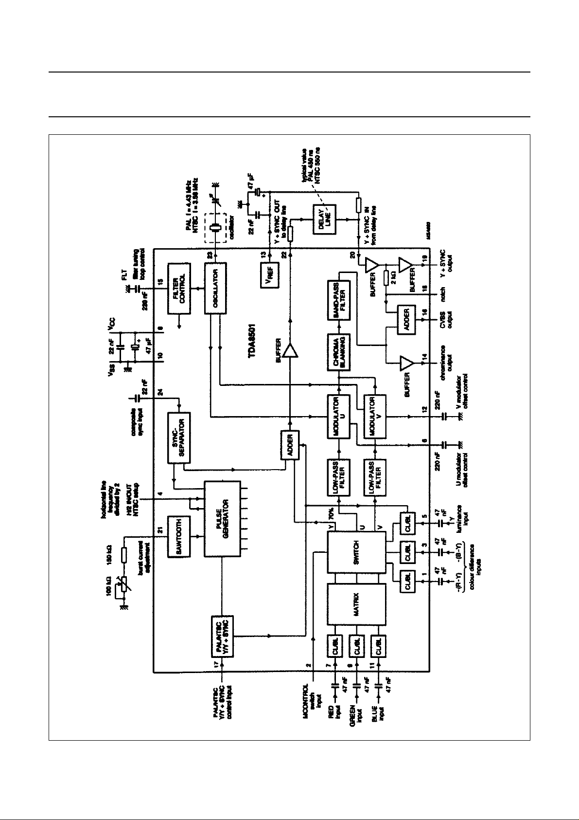
Fig.1 Block diagram.
Page 4
Philips Semiconductors Preliminary specification
PAL/NTSC encoder TDA8501
Fig.2 Pin configuration.
PINNING
U and V respectively, are the terms used to describe the colour difference signals at the output of the matrix.
SYMBOL PIN DESCRIPTION
−(R−Y) 1 colour difference input signal, for EBU bar (75%) 1.05 V (p-p)
MCONTROL 2 multiplexer switch control input; HIGH = RGB, LOW = −(R−Y), −(B−Y), Y
−(B−Y) 3 colour difference input signal, for EBU bar (75%) 1.33 V (p-p)
H/2 4 line pulse input/output divided-by-2 for synchronizing the internal H/2, if not used, this pin
dependent on mode selected, is either left open-circuit, or connected to VCC or to ground
(note 1)
Y 5 luminance input signal 1 V nominal without sync
U OFFSET 6 U modulator offset control capacitor
R 7 RED input signal for EBU bar of 75% 0.7 V (p-p)
V
CC
8 supply voltage; 5 V nominal
G 9 GREEN input signal for EBU bar of 75% 0.7 V (p-p)
V
SS
10 ground (0 V)
B 11 BLUE input signal for EBU bar of 75% 0.7 V (p-p)
V OFFSET 12 V modulator offset control capacitor
V
REF
13 2.5 V internal reference voltage output
CHROMA 14 chrominance output
FLT 15 filter tuning loop capacitor
CVBS 16 composite PAL or NTSC output, 2 V (p-p) nominal
April 1993 4
Page 5
Philips Semiconductors Preliminary specification
PAL/NTSC encoder TDA8501
SYMBOL PIN DESCRIPTION
PAL/NTSC and
Y/Y + SYNC
NOTCH 18 Y +SYNC output via an internal resistor of 2 kΩ; a notch filter can be connected to this pin
Y +SYNC OUT 19 2 V (p-p) nominal Y +SYNC output
Y +SYNC IN 20 Y +SYNC input; (from pin 22) connected to the output of the external delay line
BURST ADJ 21 burst current adjustment via external resistor
Y +SYNC OUT 22 Y +SYNC output 1 V (p-p) nominal, connected to the input of the external delay line
OSC 23 oscillator tuning: connected to either a crystal in series with capacitor to ground, or to an
CS 24 composite sync input, 0.3 V (p-p) nominal
Notes
1. Pin 4: in PAL mode, if not connected to external H2 pulse, this pin is the output for the internally generated H/2 signal.
Pin 4: in NTSC mode, for internal set-up this pin is connected to ground; when internal set-up is switched off, this pin
is connected to VCC.
2. The listed voltages connected to pin 17 (if VCC = + 5 V) enable the following Y (via pin 5) input signal states:
0 V = PAL mode; at pin 5, Y without sync and input blanking on
5 V = NTSC mode; at pin 5, Y without sync and input blanking on
1.8 V = PAL mode; at pin 5, Y with sync and input blanking off
3.2 V = NTSC mode; at pin 5, Y with sync and input blanking off
17 four level control pin (note 2)
external frequency source via a resistor in series with a capacitor
April 1993 5
Page 6

Philips Semiconductors Preliminary specification
PAL/NTSC encoder TDA8501
FUNCTIONAL DESCRIPTION
The TDA8501 device comprises:
• encoder circuit
• oscillator and filter control
• sync separator and pulse shaper.
Within this functional description, the term Y is used to
describe the luminance signal and the terms U and V
respectively, are used to describe the colour difference
signals.
Encoder circuit
INPUT STAGE
The input stage of the device uses two signal paths (see
Fig.1). Fast switching between the two signal paths is
achieved by means of the signal path selection switch
MCONTROL (pin 2).
AND G INPUT SIGNALS PATH
R, B
One signal path provides the connection for R, G and B
signal inputs (via pins 7, 9 and 11) which are connected to
a matrix via clamping and line blanking circuits. The signal
outputs from the matrix are U, V and Y.
For an EBU colour bar of 75% the amplitude of the signal
must be 0.7 V (peak-to-peak):
The Y input signal (via pin 5) differs from other signal
inputs, in that the timing of the internal clamp is after the
sync period.
The amplitude and polarity of these colour difference and
luminance input signals are processed to provide suitable
switch inputs of U, V and Y signal values.
The condition for 75% colour bar is:
pin 1 −(R−Y) = 1.05 V (peak-to-peak)
pin 3 −(B−Y) = 1.33 V (peak-to-peak)
pin 5 Y = 1 V (peak-to-peak) without sync
When selected (via MCONTROL), the U and V signals (via
the switch) are routed to the low pass filters. The Y signal
(via the switch) is routed via the adder and buffer to pin 22
(Y +SYNC OUT to delay line). Dependent on pin 17
conditioning, the Y signal may have external or internal
sync added (see section Four level control pin).
F
OUR LEVEL CONTROL PIN
The Y input signal (via pin 5) is conditioned by use of the
4-level control pin (pin 17) to emulate either the PAL or
NTSC modes, with sync and input blanking off or without
sync and input blanking on.
U = 0.493 (B−Y)
V = 0.877 (R−Y)
Y = 0.299 R +0.587 G +0.114 B
When selected (via MCONTROL), the U, V signals from
the matrix are routed through the selection switch to the
low pass filters. The Y signal from the matrix is routed
through the selection switch to the adder and combined
with the sync pulse from the sync separator and then
connected via a buffer internally to pin 22 (Y + SYNC OUT
to delay line).
−(R−Y), −(B−Y)
AND Y INPUT SIGNALS PATH
A second signal path provides the connection for negative
colour difference signal inputs−(R−Y),−(B−Y) i.e. V, U (via
pins 1, 3) and luminance Y (via pin 5), which are routed
directly to the switch inputs via clamping and line blanking
circuits.
Pin 17 may be hard wire connected to either ground (LOW
for PAL mode) or VCC (HIGH for NTSC mode). External
resistors can further modify the voltage level input at pin 17
to condition (pin 5) Y with sync and input blanking off or Y
without sync and input blanking on. (see section
PAL/NTSC and Y/Y +SYNC).
AND V SIGNALS
U
In PAL and NTSC modes the U and V (colour difference)
signals at the output of the switch are configured differently
as follows:
PAL mode:
• after the adding of the burst pulse to U and V, these
signals are connected to the input of the low pass filters.
During the vertical sync period the burst pulse is
suppressed.
NTSC mode:
• the burst pulse is only added to U and the gain of the U
and V signals is 0.95 of the gain in PAL mode. During
the vertical sync period the burst pulse is suppressed.
April 1993 6
Page 7
Philips Semiconductors Preliminary specification
PAL/NTSC encoder TDA8501
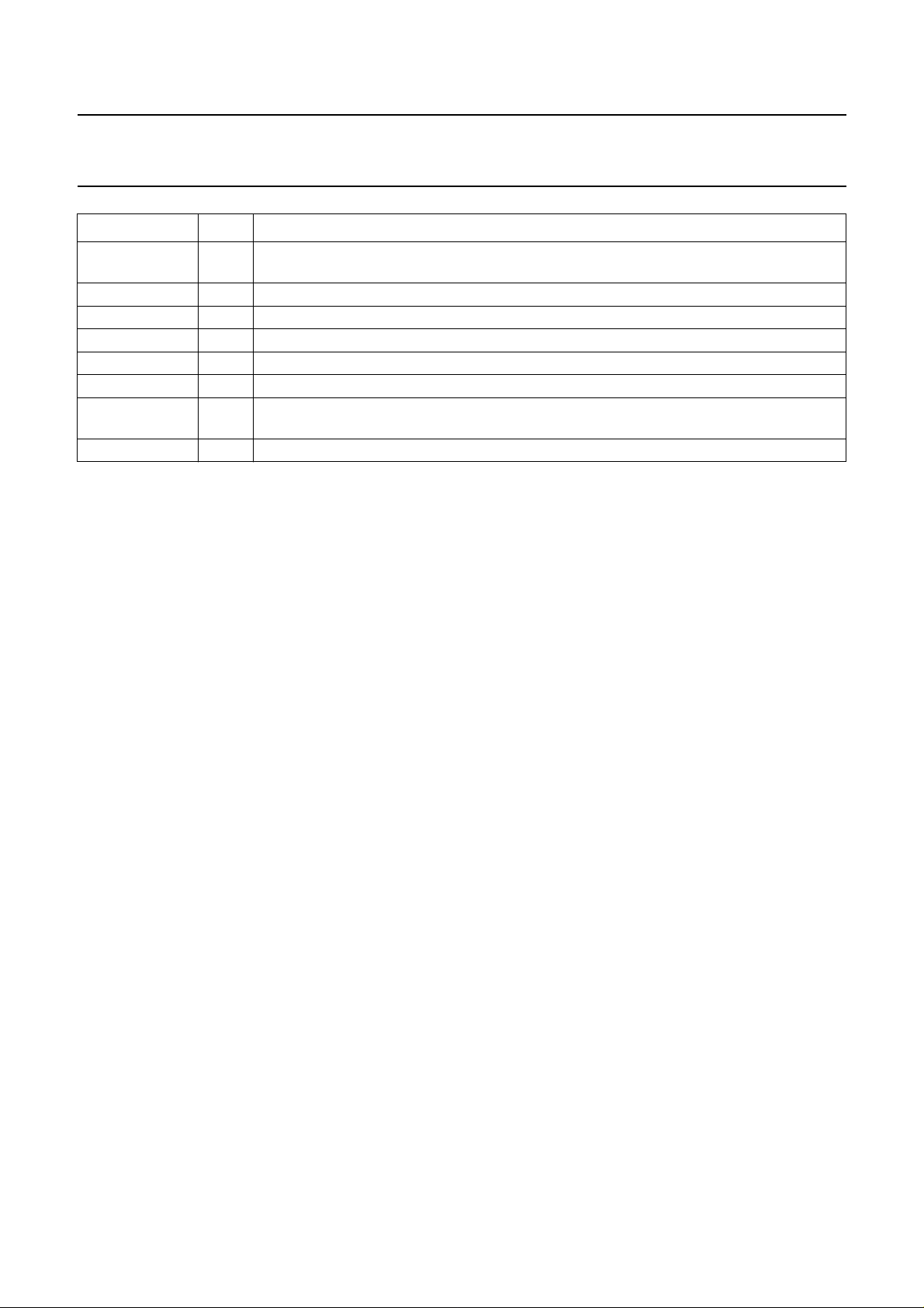
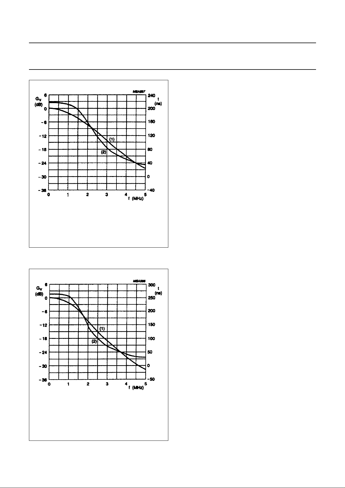
Low pass filters
The −3dB nominal frequency response level of the low
pass filters are different in PAL and NTSC modes.
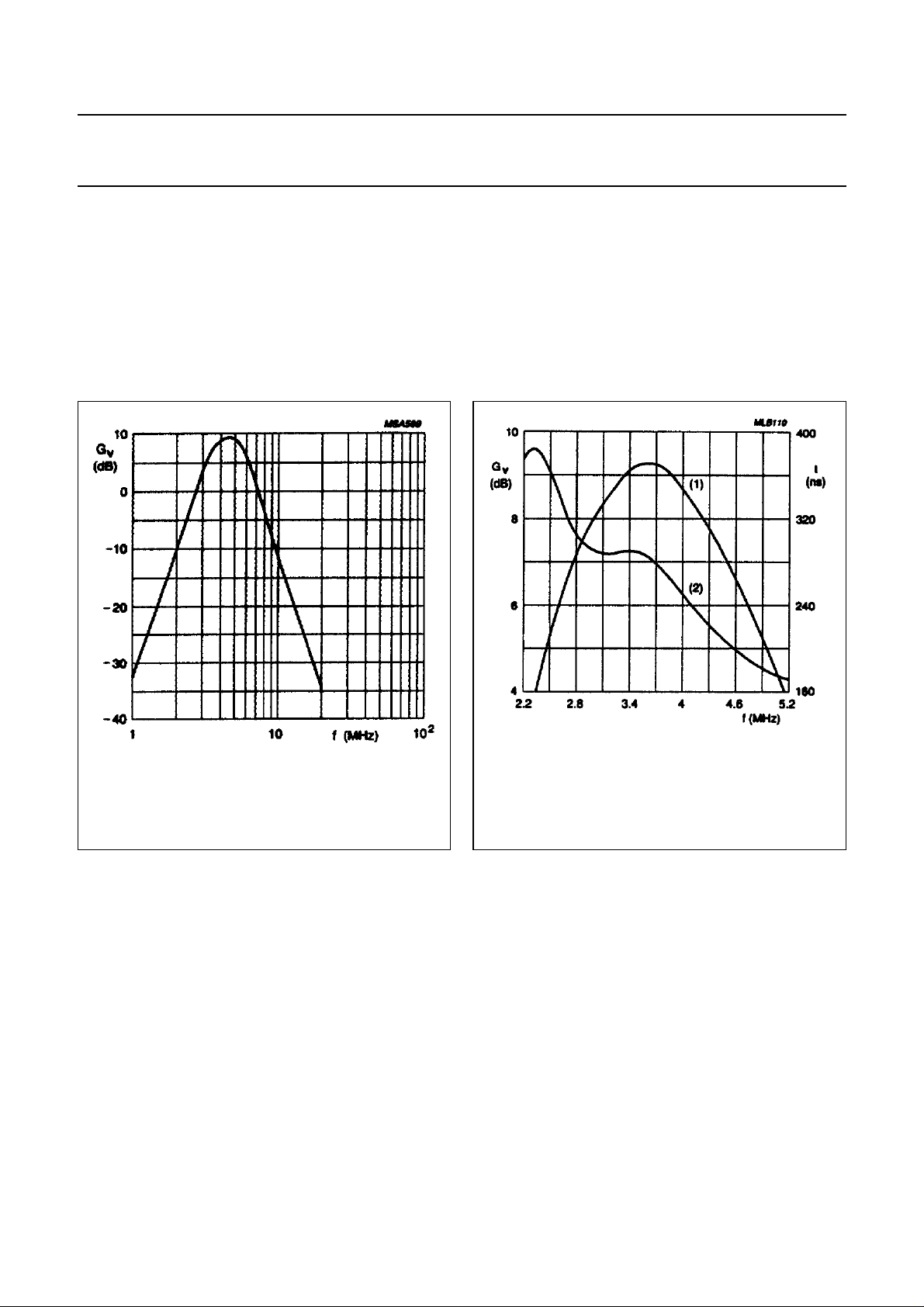
PAL mode: bandwidth = 1.35 MHz nominal (see Fig.3).
NTSC mode: bandwidth = 1.1 MHz nominal (see Fig.4).
The signal outputs of the low pass filters are connected to
the signal inputs of the U and V modulators.
U
AND VMODULATORS
Two four-quadrant multipliers are used for quadrature
amplitude modulation of the U and V signals. The level of
harmonics produced by the modulated signals are
minimal, because of real multiplication with sinewave
carriers.
The unbalance of the modulators is minimized by means
(1) frequency response.
(2) group delay.
Fig.3 Low pass filter response for colour
difference signals (PAL mode).
of a control loop and two external capacitors, pin 6 for the
U modulator and pin 12 for the V modulator. The timing of
the control loop is triggered by the H/2 pulse, so that during
one sync period the U control is active and during the next
sync period the V control is active. In this way, when U and
V are both zero, the suppressed carrier is guaranteed to be
at a low level.
(1) frequency response.
(2) group delay.
Fig.4 Low pass filter response for colour
difference signals (NTSC mode).
The internal oscillator circuit generates two sinewave
carriers (0 degree and 90 degree). The '0 degree' (0)
carrier is connected to the U modulator and the '90 degree'
(1) carrier is connected to the V modulator.
PAL mode:
• switched sequentially by the H/2 pulse, the V signal is
modulated alternately with the direct and inverse carrier.
• the internal H/2 pulse can be forced into a specific phase
by means of an external pulse connected to pin 4 (H/2).
Forcing is active at HIGH level. If not used pin 4 can be
left open-circuit or connected to ground. If pin 4 is left
open, the internally generated H/2 pulse (output) is
connected to this pin.
NTSC mode:
• alternation of the V modulation is not allowed. If pin 4 is
not used for set-up control (see Y +SYNC, CVBS and
Chrominance outputs), it can be left open-circuit or
connected to ground.
April 1993 7
Page 8
Philips Semiconductors Preliminary specification
PAL/NTSC encoder TDA8501
CHROMINANCE BLANKING
The signal outputs from the modulators are connected to
the signal input of the chrominance blanking circuit. To
avoid signal distortion that may be caused by the control
loop, the signal outputs of the modulators are blanked
during the sync period. This prevents signal distortion
during the adding of the sync pulse at the CVBS output
circuit.
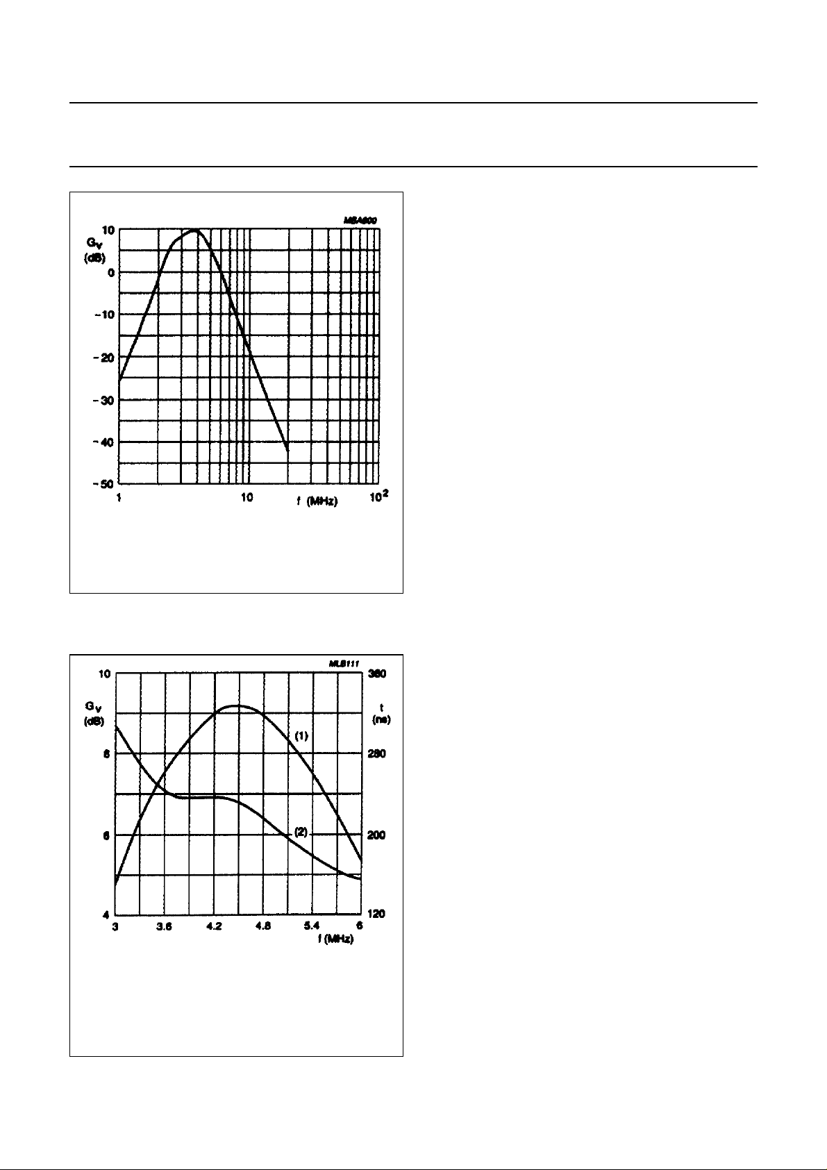
BANDPASS FILTER
A wide symmetrical bandpass filter is used so that a
maximum performance of the chrominance for Y +C
(SVHS) is guaranteed. This wide curve is possible
because of the minimal signal level of the harmonics within
the modulators see Figs (PAL mode: 5 and 6);
(NTSC mode: 7 and 8) which illustrate the nominal
response for PAL and NTSC modes.
Fig.5 Band pass filter nominal frequency
response (PAL mode).
(1) frequency response.
(2) group delay.
Fig.6 Band pass filter nominal frequency/group
delay response (PAL mode).
April 1993 8
Page 9
Philips Semiconductors Preliminary specification
PAL/NTSC encoder TDA8501
Y +SYNC, CVBS AND CHROMINANCE OUTPUTS
The Y signal from the matrix, or the Y signal from pin 5,
(selected via the switch) is added with the composite sync
signal of the sync separator (dependent on pin 17
conditioning). The output of the adder, nominal 1 V
(peak-to-peak), is connected to pin 22 (see Fig.1). Pin 22
is connected to an external delay line.
The delay line is necessary for correct timing of the
Y + SYNC signal with the chrominance signal. The output
Fig.7 Band pass filter nominal frequency
response (NTSC mode).
resistor of the delay line is connected to V
output of the external delay line is connected to (input)
pin 20.
The Y +SYNC (delayed) input signal at pin 20 is amplified
via a buffer to a level of 2 V (peak-to-peak) nominal and
connected to pin 19 (Y + SYNC output).
The Y + SYNC (delayed) input signal at pin 20 is also
connected via an internal resistor of 2 kΩ to the input of the
CVBS adder stage. After the internal resistor of 2 kΩ, and
before the input of the CVBS adder, an external notch filter
can be connected via pin 18.
The chrominance output of the bandpass filter is added
with Y +SYNC signal via the CVBS adder. The CVBS
(combined video and blanking signal) output of the adder
is connected to pin 16 with a nominal amplitude of 2 V
(peak-to-peak).
(pin 13). The
REF
(1) frequency response.
(2) group delay.
Fig.8 Band pass filter nominal frequency/group
delay response (NTSC mode).
The chrominance output of the bandpass filter is amplified
via a buffer and connected to pin 14. The chrominance
amplitude corresponds with the value of Y + SYNC signal
output at pin 19. Together both outputs give the
Y +C (SVHS) signals.
B
LACK AND BLANKING LEVELS IN PAL AND NTSC MODES
PAL mode: Fig.9 illustrates the nominal Y + SYNC signal
at pin 22, the difference between black and blanking level
is 0 mV.
NTSC mode: Fig.10 illustrates the nominal Y + SYNC
signal at pin 22, the difference between black and blanking
level is 53 mV.
Because of the difference between the black and blanking
level in the NTSC mode, there are two options for NTSC.
April 1993 9
Page 10

Philips Semiconductors Preliminary specification
PAL/NTSC encoder TDA8501
NTSC option with internal set-up generation
Pin 4 connected to ground or left open-circuit. The set-up
is generated internally and the input signals have the
values already specified in section Input stage. The set-up
is not suppressed during vertical sync.
NTSC option without internal set-up generation
Pin 4 connected to VCC. This option places some
restrictions on the input signals as follows:
• if the output signal must be according to the NTSC
standard, the input signals must be generated with a
specific set-up level
• for R, G and B inputs a set-up level of 53 mV is required,
therefore the specified amplitude must be 753 mV
(peak-to-peak) instead of 700 mV (peak-to-peak)
• for U, V and Y inputs a set-up level for Y of 76 mV is
required, therefore the specified amplitude must be
1076 mV (peak-to-peak) (without sync) instead of 1 V
(peak-to-peak). This option, combined with U, V and Y
Fig.9 Nominal Y + SYNC signal level at pin 22
(PAL mode).
inputs, is not possible if VCC is < 4.75 V.
Fig.10 Nominal Y +SYNC signal level at pin 22
(NTSC mode).
April 1993 10
Page 11

Philips Semiconductors Preliminary specification
PAL/NTSC encoder TDA8501
Oscillator and Filter Control
The internal crystal oscillator is connected to pin 23 which
provides for the external connection of a crystal in series
with a trimmer to ground. It is possible to connect an
external signal source to pin 23, via a capacitor in series
with a resistor. The signal shape is not important.
Figure 11 shows the external components connected to
pin 23 and the required conditions. The minimum AC
current of 50 µA must be determined by the resistors
(R
and R
int
) and the voltage of the signal source. For
ext
example, in this way an external sub-carrier, locked to the
sync, can be used.
PAL mode: frequency of the oscillator is
4.433618 MHz.
NTSC mode: frequency of the oscillator is
3.579545 MHz.
The −3 dB of the low pass filters and the centre frequency
of the bandpass filter are controlled by the filter control
loop and directly coupled to the value of the frequency of
the oscillator. The external capacitor of the control loop is
connected to pin 15.
Sync separator and Pulse shaper
The composite sync (CS) input at pin 24 (via the sync
separator) together with a sawtooth generator provide the
source for all pulses necessary for the processing.
Pulses are used for:
• clamping
• video blanking
• H/2
• chrominance blanking
• burst pulse generation for adding to U, V
• pulses for the modulator offset control.
The value of the sawtooth generator output (current) is
determined by the value of a fixed resistor to ground which
is connected externally at pin 21 (BURST ADJ). When
finer tolerance of the burst position is required, the fixed
resistor is connected in series with a variable
potentiometer to ground. By use of the potentiometer the
burst position at the outputs can be finely adjusted, after
which the pulse width of the burst and the position and
pulse width of all other internal pulses are then
determined. When using a fixed resistor with a tolerance of
2%, a tolerance of 10% of the burst position can be
expected. Timing diagrams of the pulses are provided by
Figs 12 and 13.
Fig.11 Tuning circuit for external signal source.
H/2 at pin 4 is only necessary in the PAL mode when the
internal H/2 pulse requires locking with an external H/2
phase (two or more encoders locked in same phase). The
forcing of the internal H/2 to a desired phase is possible by
means of an external pulse. Forcing is active at HIGH
level.
For the functioning of Pin 4 in the NTSC mode see also
section Black and Blanking levels in PAL and NTSC
modes.
April 1993 11
Page 12

Philips Semiconductors Preliminary specification
PAL/NTSC encoder TDA8501
April 1993 12
Fig.12 Sync separator and pulse shaper pulses.
Page 13

Philips Semiconductors Preliminary specification
PAL/NTSC encoder TDA8501
April 1993 13
Fig.13 Sync separator and pulse shaper pulse timing levels.
Page 14

Philips Semiconductors Preliminary specification
PAL/NTSC encoder TDA8501
PAL/NTSC and Y/Y + SYNC
Pin 17 is used as a four level control pin to condition the Y/Y + SYNC input signal (via pin 5). Pin 17 is normally connected
to ground for PAL mode, or to VCC for the NTSC mode. By use of external resistors (potential divider connected to
pin 17), the input blanking at pin 5 can be switched on and off. (see Table 1 and Fig 14).
Table 1 PAL/NTSC Y/Y +SYNC pin 5 options (pin 17 connection configurations).
MODE PIN 5 STATUS PIN 17 CONNECTION REQUIREMENT
PAL Y without sync and input blanking on pin 17 LOW, connected to V
NTSC Y without sync and input blanking on pin 17 HIGH, connected to V
PAL Y with sync and input blanking off pin 17 with 39 kΩ connected to VCC and 22 kΩ connected to V
NTSC Y with sync and input blanking off pin 17 with 22 kΩ connected to VCC and 39 kΩ connected to V
LIMITING VALUES
In accordance with the Absolute Maximum System (IEC134); all voltages referenced to V
SYMBOL PARAMETER MIN. MAX. UNIT
V
CC
T
stg
T
amb
positive supply voltage 0 5.5 V
storage temperature −65 +150 °C
operating ambient temperature −25 +70 °C
SS
CC
(pin 10).
SS
SS
SS
THERMAL RESISTANCE
SYMBOL PARAMETER THERMAL RESISTANCE
R
th j-a
from junction to ambient in free air
SOT234 66 K/W
SOT137 75 K/W
DC CHARACTERISTICS
V
= 5 V; T
CC
= 25 °C; all voltages referenced to ground (pin 10); unless otherwise specified.
amb
SYMBOL PARAMETER CONDITIONS MIN. TYP. MAX. UNIT
Supply (pin 8)
V
I
P
V
CC
CC
tot
REF
supply voltage 4.5 5.0 5.5 V
supply current − 40 − mA
total power dissipation − 200 − mW
reference voltage output (pin 13) 2.425 2.5 2.575 V
April 1993 14
Page 15

Philips Semiconductors Preliminary specification
PAL/NTSC encoder TDA8501
AC CHARACTERISTICS
= 5 V; T
V
CC
SYMBOL PARAMETER CONDITIONS MIN. TYP. MAX. UNIT
Encoder circuit
Input stage (pins 1, 3, 5, 7, 9 and 11); black level = clamping level
V
n(max)
V
n(min)
I
bias
V
I
input clamping impedance
Z
I
G gain tolerance of Y, −(R−Y) and
= 25 °C; composite sync signal connected to pin 24; unless otherwise specified.
amb
maximum signal
from black level positive − 1.2 − V
from black level negative only pins 1, 3 and 5 − 0.9 − V
input bias current VI = V
13
input voltage clamped input capacitor
−−< 1 µA
tbf V
13
tbf V
connected to ground
I
= 1 mA − 80 −Ω
I
= 1 mA − 80 −Ω
I
O
matrix and gain tolerance of R, G
−−< 5%
and B signals
−−< 5%
−(B−Y)
MCONTROL (pin 2; note 1)
V
IL
LOW level input voltage
Y, −(R−Y) and −(B−Y)
V
IH
HIGH level input voltage
R, G and B
I
I
t
sw
input current −−−3µA
switching time − 50 − ns
U modulator offset control (pin 6)
V
6
I
LI
V
LL
V
HL
DC voltage control level − 2.5 − V
input leakage current −−100 nA
limited level voltage LOW − 1.8 − V
limited level voltage HIGH − 3.2 − V
V modulator offset control (pin 12)
V
12
I
LI
V
LL
V
HL
DC voltage control level − 2.5 − V
input leakage current −−100 nA
limited level voltage LOW − 1.8 − V
limited level voltage HIGH − 3.2 − V
Y + SYNC (pin 22 out to delay circuit)
R
O
I
sink
I
source
V
BL
output resistance −−< 25 Ω
maximum sink current 350 −−µA
maximum source current 1000 −−µA
black level output voltage − 2.5 − V
0 − 0.4 V
1 − 5V
April 1993 15
Page 16

Philips Semiconductors Preliminary specification
PAL/NTSC encoder TDA8501
SYMBOL PARAMETER CONDITIONS MIN. TYP. MAX. UNIT
PAL mode; pin 17 = 0 V
V
SYNC
V
Y
V
DIF
NTSC mode; pin 17 = 5 V and pin 4 open-circuit or ground
V
SYNC
V
Y
V
DIF
BW frequency response pin 22 with external
t
d
t
d
α Chrominance cross talk 0 dB = 1330 mV
sync voltage amplitude 285 300 315 mV
Y voltage amplitude 665 700 735 mV
difference between black and
− 0 − mV
blanking level
sync voltage amplitude 270 286 300 mV
Y voltage amplitude 628 661 694 mV
difference between black and
− 53 − mV
blanking level
10 −−MHz
load of R = 10 kΩ and
C = 10 pF
group delay tolerance −−20 ns
sync delay from pin 24 to pin 22 220 290 360 ns
Y delay from pin 5 to pin 22 − 10 − ns
−−−60 dB
(peak-to-peak)
= 75% RED
Y + SYNC IN (pin 20 from delay circuit; note 2)
I
bias
V
I
input bias current −−1µA
maximum voltage amplitude −−1V
Y + SYNC OUT (pin 19 output Y (SVHS); note 2)
R
O
I
sink
I
source
V
BL
output resistance − 120 −Ω
maximum sink current 650 −−µA
maximum source current 1000 −−µA
black level output voltage − 1.65 − V
GY+ SYNC gain;
from pin 20 to pin 19
BW frequency response pin 19 with external
load of R = 10 kΩ and
C = 10 pF
group delay tolerance −−20 ns
α Chrominance cross talk 0 dB = 1330 mV
(peak-to-peak)
= 75% RED
− 12 − dB
10 −−MHz
−−−54 dB
April 1993 16
Page 17

Philips Semiconductors Preliminary specification
PAL/NTSC encoder TDA8501
SYMBOL PARAMETER CONDITIONS MIN. TYP. MAX. UNIT
NOTCH (pin 18)
R
O
V
CC
I
sink
Chrominance output (pin 14)
I
sink
I
source
R
O
∆V
DC
PAL mode; pin 17 = 0 V
V
O
NTSC mode; pin 17 = 5 V
V
O
LPF Low-pass filters see Figs 3 and 4
BPF Band-pass filters see Figs 5 and 6
V
n
BP burst phase; 0 degrees = phase U carrier
α Y + SYNC cross talk
output resistance 1750 2000 2500 Ω
DC voltage level − 2.5 − V
maximum sink current 350 −−µA
maximum sink current 700 −−µA
maximum source current 1000 −−µA
output resistance − 120 −Ω
variation of DC voltage level
−−5mV
when chrominance signal is
blanked and chrominance signal is
not blanked
chrominance output voltage
480 600 720 mV
(peak-to-peak) amplitude burst
ratio: chrominance
2.1 2.2 2.3
(75% RED)/burst
chrominance output voltage
460 570 680 mV
(peak-to-peak) amplitude burst
ratio: chrominance
2.1 2.2 2.3
(75% RED)/burst
carrier suppression when
input-signals are 0 V
phase accuracy (difference
0 dB = 1330 mV
(peak-to-peak)
− 37 − dB
−−2 degrees
between 0 and 90 degree carriers)
noise level (RMS value) −−4mV
PAL mode −±135 − degrees
NTSC mode − 180 − degrees
(0 to 6 MHz)
0 dB = 1400 mV
(peak-to-peak)
−−−60 dB
April 1993 17
Page 18

Philips Semiconductors Preliminary specification
PAL/NTSC encoder TDA8501
SYMBOL PARAMETER CONDITIONS MIN. TYP. MAX. UNIT
CVBS output (pin 16)
I
sink
I
source
V
O
G Y +SYNC gain;
G chrominance difference;
G
ø
G
V
R
O
Oscillator output (pin 23)
OSC series-resonance the resonance resistance of the crystal should be < 60 Ω and the
maximum sink current 650 −−µA
maximum source current 1000 −−µA
DC voltage level Y +SYNC = 0 − 1.6 − V
− 12 − dB
from pin 20 to pin 16
− 0 − dB
from pin 14 to pin 16
differential phase note 3 −−3 degrees
differential gain note 4 −−3dB
output resistance − 120 −Ω
parallel capacitance of the crystal should be < 10 pF.
Filter tuning loop (pin 15)
V
V
V
V
DC
DC
DCL
DCH
DC control voltage level NTSC − 0.83 − V
DC control voltage level PAL − 0.88 − V
limited DC-level LOW IO = 200 µA − 0.27 − V
limited DC-level HIGH II = 200 µA − 1.8 − V
H2 (pin 4)
V
IL
V
IH
I
I
I
O
V
O
V
O
I
sink
I
source
LOW level input voltage inactive 0 − 1V
HIGH level input voltage active 4 − 5V
current for forcing HIGH 220 −−µA
current for forcing LOW 260 −−µA
voltage out LOW −−< 0.5 V
voltage out HIGH 4 −−V
maximum sink current 50 −−µA
maximum source current 50 −−µA
Composite sync input (pin 24)
V
SYNC
SYNC pulse amplitude 75 300 600 mV (p-p)
slicing level − 50 − %
I
I
I
O
input current − 4 −µA
maximum output current during
SYNC
− 100 −µA
BURST ADJ (pin 21; note 5)
BP DC voltage level − V
April 1993 18
REF
(V13)
− V
Page 19

Philips Semiconductors Preliminary specification
PAL/NTSC encoder TDA8501
SYMBOL PARAMETER CONDITIONS MIN. TYP. MAX. UNIT
Control pin PAL/NTSC and Y/Y + SYNC (pin 17; note 6)
V
I
V
I
V
I
V
I
I
bias
Notes
1. The threshold level of this pin is 700 mV ±20 mV. The specification of the HIGH and LOW levels is according to the
SCART fast blanking.
2. Pin 20 condition: black level of input signal must be 2.5 V; amplitude 0.5 V (peak-to-peak) nominal.
3. Definition:
PAL mode and blanking pin 5
0 − 1V
active
internal sync added to Y
PAL mode and blanking pin 5
1.6 − 2.0 V
inactive
internal sync not added to Y
NTSC mode and blanking pin 5
4 − 5V
active
internal sync added to Y
NTSC mode and blanking pin 5
3 − 3.4 V
inactive
internal sync not added to Y
input bias current −−−10 µA
maximum phase−minimum phase=difference phase
4. Definition:
maximum gain minimum gain–
---------------------------------------------------------------------------------maximum gain
100× difference gain %=
5. The output impedance of this pin is low (< 100 Ω). The nominal value of the external resistor is 196 kΩ (see also
section Sync separator and Pulse shaper).
6. The threshold levels are: 0.25 times V
, 0.5 times VCC and 0.75 times VCC.
CC
April 1993 19
Page 20

Philips Semiconductors Preliminary specification
PAL/NTSC encoder TDA8501
Table 2 Internal circuitry.
PIN NAME CIRCUIT DESCRIPTION
1 −(R−Y) −(R−Y) input; connected via
47 nF capacitor
1.05 V (p-p) for EBU bar of 75%
see also pins 3, 5, 7, 9 and 11
2 MCONTROL multiplexer switch control input
< 0.4 V Y, U and V
>1 V R, G and B
3 −(B−Y) see pin 1 −(B−Y) input; connected via
47 nF capacitor
1.33 (p-p) for EBU bar of 75%
4 H/2
IN/OUT
H/2 input
PAL MODE:
pin open, output of internal H/2
Forcing possibility
NTSC mode:
0 V set-up
5 V no set-up
April 1993 20
Page 21

Philips Semiconductors Preliminary specification
PAL/NTSC encoder TDA8501
PIN NAME CIRCUIT DESCRIPTION
5 Y see pin 1 Y input; connected via 47 nF
capacitor
1 V (p-p) for EBU bar of 75%
6 U OFFSET 220 nF (low-leakage) connected
to ground see also pin 12
7 R see pin 1 RED input; connected via 47 nF
capacitor
0.7 V (p-p) for EBU bar of 75%
8V
9 G see pin 1 GREEN input; connected via
10 V
CC
SS
supply voltage
5 V nominal
47 nF capacitor
0.7 V (p-p) for EBU bar of 75%
ground
11 B see pin 1 BLUE input; connected via
47 nF capacitor
0.7 V (p-p) for EBU bar of 75%
April 1993 21
Page 22

Philips Semiconductors Preliminary specification
PAL/NTSC encoder TDA8501
PIN NAME CIRCUIT DESCRIPTION
12 V OFFSET see pin 6 220 nF (low-leakage) connected
to ground
13 V
REF
2.5 V reference voltage
decoupling with 47 µF and 22 nF
capacitors
14 CHROMA chrominance output; together with
pin 19 the Y + C (SVHS) output
15 FLT filter control pin
220 nF capacitor to ground
April 1993 22
Page 23

Philips Semiconductors Preliminary specification
PAL/NTSC encoder TDA8501
PIN NAME CIRCUIT DESCRIPTION
16 CBVS CVBS output
17 PAL/NTSC
Y/Y+SYNC
18 NOTCH pin for external notch filter
4-level control pin
Pin 5:
0 V PAL, Y
1.8 V PAL Y+SYNC
3.2 V NTSC Y +SYNC
5 V NTSC Y
April 1993 23
Page 24

Philips Semiconductors Preliminary specification
PAL/NTSC encoder TDA8501
PIN NAME CIRCUIT DESCRIPTION
19 Y+SYNC OUT output of the Y +SYNC signal;
together with pin 14 the Y +C
(SVHS) output
20 Y+SYNC IN input of the delayed Y+SYNC
signal of the delay line
black level must be 2.5 V
21 BURST ADJ external resistor to ground for
adjusting the position of the burst
April 1993 24
Page 25

Philips Semiconductors Preliminary specification
PAL/NTSC encoder TDA8501
PIN NAME CIRCUIT DESCRIPTION
22 Y+SYNC OUT output of the Y+SYNC signal,
connected to the delay line via a
resistor
23 OSC subcarrier-crystal in series with a
trimmer, or an external
subcarrier signal, via 1 nF in
series with a resistor
24 CS composite SYNC signal input
amplitude < 600 mV (p-p)
April 1993 25
Page 26

Philips Semiconductors Preliminary specification
PAL/NTSC encoder TDA8501
April 1993 26
Fig.14 Application diagram.
Page 27

Philips Semiconductors Preliminary specification
PAL/NTSC encoder TDA8501
PACKAGE OUTLINES
SDIP24: plastic shrink dual in-line package; 24 leads (400 mil)
D
seating plane
L
Z
24
pin 1 index
e
b
b
1
13
SOT234-1
M
E
A
2
A
A
1
w M
c
E
(e )
M
1
H
1
0 5 10 mm
scale
DIMENSIONS (mm are the original dimensions)
A
A
A
UNIT b
Note
1. Plastic or metal protrusions of 0.25 mm maximum per side are not included.
mm
OUTLINE
VERSION
SOT234-1
max.
4.7 0.51 3.8
12
min.
max.
IEC JEDEC EIAJ
1.3
0.8
b
1
0.53
0.40
REFERENCES
cEe M
0.32
0.23
(1) (1)
D
22.3
21.4
April 1993 27
9.1
8.7
12
(1)
Z
L
3.2
2.8
EUROPEAN
PROJECTION
M
10.7
10.2
E
12.2
10.5
e
1
w
H
0.181.778 10.16
ISSUE DATE
92-11-17
95-02-04
max.
1.6
Page 28

Philips Semiconductors Preliminary specification
PAL/NTSC encoder TDA8501
SO24: plastic small outline package; 24 leads; body width 7.5 mm
D
c
y
Z
24
pin 1 index
1
e
13
12
w M
b
p
SOT137-1
E
H
E
Q
A
2
A
1
L
p
L
detail X
(A )
A
X
v M
A
A
3
θ
0 5 10 mm
scale
DIMENSIONS (inch dimensions are derived from the original mm dimensions)
mm
OUTLINE
VERSION
SOT137-1
A
max.
2.65
0.10
A
1
0.30
0.10
0.012
0.004
A2A
2.45
2.25
0.096
0.089
IEC JEDEC EIAJ
075E05 MS-013AD
0.25
0.01
b
3
p
0.49
0.32
0.36
0.23
0.019
0.013
0.014
0.009
UNIT
inches
Note
1. Plastic or metal protrusions of 0.15 mm maximum per side are not included.
(1)E(1) (1)
cD
15.6
7.6
7.4
0.30
0.29
1.27
0.050
15.2
0.61
0.60
REFERENCES
April 1993 28
eHELLpQ
10.65
10.00
0.419
0.394
1.4
0.055
1.1
0.4
0.043
0.016
1.1
1.0
0.043
0.039
PROJECTION
0.25
0.25 0.1
0.01
0.01
EUROPEAN
ywv θ
Z
0.9
0.4
8
0.004
ISSUE DATE
0.035
0.016
95-01-24
97-05-22
0
o
o
Page 29

Philips Semiconductors Preliminary specification
PAL/NTSC encoder TDA8501
SOLDERING
Introduction
There is no soldering method that is ideal for all IC
packages. Wave soldering is often preferred when
through-hole and surface mounted components are mixed
on one printed-circuit board. However, wave soldering is
not always suitable for surface mounted ICs, or for
printed-circuits with high population densities. In these
situations reflow soldering is often used.
This text gives a very brief insight to a complex technology.
A more in-depth account of soldering ICs can be found in
“IC Package Databook”
our
(order code 9398 652 90011).
SDIP
SOLDERING BY DIPPING OR BY WAVE
The maximum permissible temperature of the solder is
260 °C; solder at this temperature must not be in contact
with the joint for more than 5 seconds. The total contact
time of successive solder waves must not exceed
5 seconds.
The device may be mounted up to the seating plane, but
the temperature of the plastic body must not exceed the
specified maximum storage temperature (T
stg max
). If the
printed-circuit board has been pre-heated, forced cooling
may be necessary immediately after soldering to keep the
temperature within the permissible limit.
R
EPAIRING SOLDERED JOINTS
Apply a low voltage soldering iron (less than 24 V) to the
lead(s) of the package, below the seating plane or not
more than 2 mm above it. If the temperature of the
soldering iron bit is less than 300 °C it may remain in
contact for up to 10 seconds. If the bit temperature is
between 300 and 400 °C, contact may be up to 5 seconds.
SO
REFLOW SOLDERING
Reflow soldering techniques are suitable for all SO
packages.
Several techniques exist for reflowing; for example,
thermal conduction by heated belt. Dwell times vary
between 50 and 300 seconds depending on heating
method. Typical reflow temperatures range from
215 to 250 °C.
Preheating is necessary to dry the paste and evaporate
the binding agent. Preheating duration: 45 minutes at
45 °C.
AVE SOLDERING
W
Wave soldering techniques can be used for all SO
packages if the following conditions are observed:
• A double-wave (a turbulent wave with high upward
pressure followed by a smooth laminar wave) soldering
technique should be used.
• The longitudinal axis of the package footprint must be
parallel to the solder flow.
• The package footprint must incorporate solder thieves at
the downstream end.
During placement and before soldering, the package must
be fixed with a droplet of adhesive. The adhesive can be
applied by screen printing, pin transfer or syringe
dispensing. The package can be soldered after the
adhesive is cured.
Maximum permissible solder temperature is 260 °C, and
maximum duration of package immersion in solder is
10 seconds, if cooled to less than 150 °C within
6 seconds. Typical dwell time is 4 seconds at 250 °C.
A mildly-activated flux will eliminate the need for removal
of corrosive residues in most applications.
EPAIRING SOLDERED JOINTS
R
Fix the component by first soldering two diagonally-
opposite end leads. Use only a low voltage soldering iron
(less than 24 V) applied to the flat part of the lead. Contact
time must be limited to 10 seconds at up to 300 °C. When
using a dedicated tool, all other leads can be soldered in
one operation within 2 to 5 seconds between
270 and 320 °C.
Reflow soldering requires solder paste (a suspension of
fine solder particles, flux and binding agent) to be applied
to the printed-circuit board by screen printing, stencilling or
pressure-syringe dispensing before package placement.
April 1993 29
Page 30

Philips Semiconductors Preliminary specification
PAL/NTSC encoder TDA8501
DEFINITIONS
Data sheet status
Objective specification This data sheet contains target or goal specifications for product development.
Preliminary specification This data sheet contains preliminary data; supplementary data may be published later.
Product specification This data sheet contains final product specifications.
Limiting values
Limiting values given are in accordance with the Absolute Maximum Rating System (IEC 134). Stress above one or
more of the limiting values may cause permanent damage to the device. These are stress ratings only and operation
of the device at these or at any other conditions above those given in the Characteristics sections of the specification
is not implied. Exposure to limiting values for extended periods may affect device reliability.
Application information
Where application information is given, it is advisory and does not form part of the specification.
LIFE SUPPORT APPLICATIONS
These products are not designed for use in life support appliances, devices, or systems where malfunction of these
products can reasonably be expected to result in personal injury. Philips customers using or selling these products for
use in such applications do so at their own risk and agree to fully indemnify Philips for any damages resulting from such
improper use or sale.
April 1993 30
 Loading...