

Page 1

INTEGRATED CIRCUITS
DATA SH EET
TDA8446
Fast RGB/YC switch for digital
decoding
Product specification
Supersedes data of August 1992
File under Integrated Circuits, IC02
Philips Semiconductors
1995 Feb 16
Page 2

Philips Semiconductors Product specification
Fast RGB/YC switch for digital decoding TDA8446
FEA TURES
• R, G, B clamped inputs
• Luminance and chrominance difference matrix
• Y-clamped inputs
• Fast switching between internal and external Y
• Chrominance input
• Amplifier with selectable gain
• 3-state switch for chrominance output.
APPLICATIONS
• Digital TV systems
• Desktop video architecture.
QUICK REFERENCE DATA
SYMBOL PARAMETER MIN. TYP. MAX. UNIT
V
CC
T
amb
ORDERING INFORMATION
supply voltage 10.8 − 13.2 V
operating ambient temperature 0 − +70 °C
DESCRIPTION
The TDA8446 is a video switch which has been designed
for use in Digital Multistandard System Decoders (DMSD)
in digital video system. The device is intended for matrixing
incoming RGB signals and for switching between
luminance signals. It generates a SYNC signal and TTL
clamping pulses from any video signal with sync pulses.
TYPE NUMBER
NAME DESCRIPTION VERSION
TDA8446 DIP20 plastic dual in-line package; 20 leads; (300 mil) SOT146-1
TDA8446T SO28 plastic small outline package; 28 leads; body width 7.5 mm SOT136-1
PACKAGE
1995 Feb 16 2
Page 3
Philips Semiconductors Product specification
Fast RGB/YC switch for digital decoding TDA8446
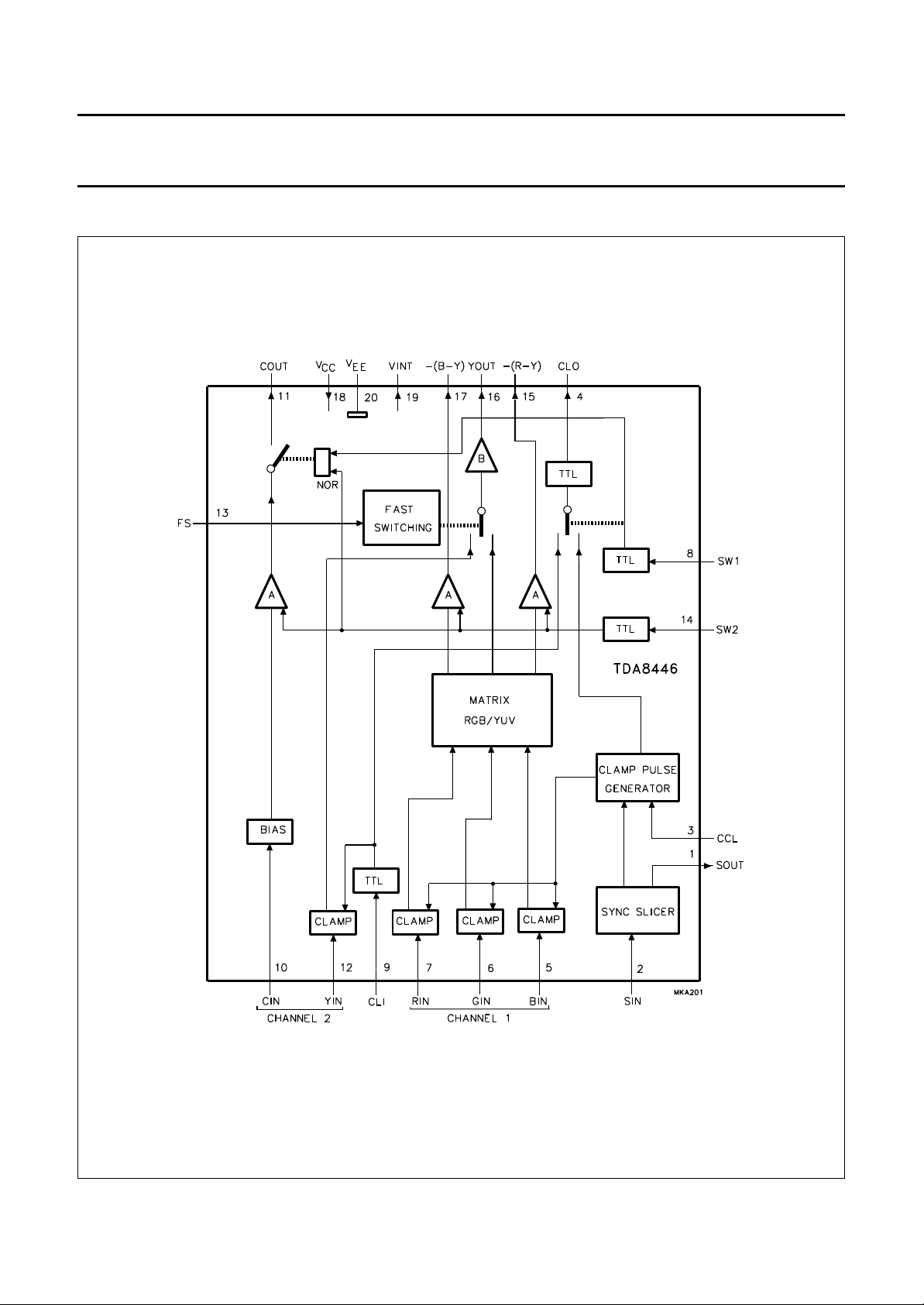
BLOCK DIAGRAM
Fig.1 Block diagram (TDA8446).
1995 Feb 16 3
Page 4

Philips Semiconductors Product specification
Fast RGB/YC switch for digital decoding TDA8446
PINNING
SYMBOL
SOUT 1 1 synchronization signal output; this output provides the synchronization information
SIN 2 2 synchronization signal input; CSYNC or CVBS signal from the peri-connector
CCL 3 3 clamping capacitor connection; the clamping pulse is generated by external circuitry
n.c. − 4 not connected
CLO 4 5 clamping pulse output
n.c. − 6 not connected
BIN 5 7 B-signal input
GIN 6 8 G-signal input
RIN 7 9 R-signal input
SW1 8 10 clamping control signal input; this TTL signal is used to select the clamp signal, a LOW
n.c. − 11 not connected
CLI 9 12 clamping pulse input; this TTL signal indicates the black level clamping period for the
CIN 10 13 chrominance signal input
COUT 11 14 chrominance signal output
YIN 12 15 luminance signal input; this input also accepts the CVBS signal
FS 13 16 fast switching signal input; this signal is used to control fast switching of the luminance
n.c. − 17 not connected
n.c. − 18 not connected
SW2 14 19 gain control signal input; this TTL signal is used to set the gain of the chrominance
n.c. − 20 not connected
−(R-Y) 15 21 −(R−Y) signal output
YOUT 16 22 luminance signal output
−(B−Y) 17 23 −(B−Y) signal output
n.c. − 24 not connected
n.c. − 25 not connected
V
CC
VINT 19 27 internal decoupling
V
EE
PIN
DESCRIPTION
DIP20 SO28
extracted from the incoming signal at pin 2 (SIN).
connected to this pin, the generated pulse clamps the RGB inputs.
level at this input forces the circuit to output the generated clamping pulse.
incoming Y signal (active-HIGH).
signals, a HIGH level at this input forces the circuit to output the internal Y signal.
amplifiers (A), a LOW level at this input forces the gain A to 6 dB (HIGH forces to 0 dB).
18 26 positive supply voltage (+12 V)
20 28 ground
1995 Feb 16 4
Page 5

Philips Semiconductors Product specification
Fast RGB/YC switch for digital decoding TDA8446
Fig.2 Pin configuration (DIP20). Fig.3 Pin configuration (SO28).
1995 Feb 16 5
Page 6

Philips Semiconductors Product specification
Fast RGB/YC switch for digital decoding TDA8446
LIMITING VALUES
In accordance with the Absolute Maximum Rating System (IEC 134).
SYMBOL PARAMETER MIN. MAX. UNIT
V
CC
V
I
T
stg
HANDLING
Each pin will withstand the ESD test in accordance with MIL-STD-883C class 2 (2000 V to 2999 V). Method 3015
(Human body model: R = 1500 Ω; C = 100 pF) 3 pulses positive and 3 pulses negative on each pin as a function of
ground. The IC will withstand 500 V in accordance with UZW-BO/FQ-B302 (Machine model: R = 0 Ω; C = 200 pF;
L = 2.5 µH) 3 pulses positive and 3 pulses negative.
OPERATING CHARACTERISTICS
supply voltage −0.3 +14 V
input voltage −0.3 +12.3 V
storage temperature −55 +125 °C
SYMBOL PARAMETER MIN. TYP. MAX. UNIT
Supply/temperature
V
CC
T
amb
supply voltage 10.8 − 13.2 V
operating ambient temperature 0 − +70 °C
TTL inputs (SW1, SW2 and CLI)
V
IH
V
IL
HIGH level input voltage 2 − V
CC
LOW level input voltage −0.3 − +0.8 V
V
SYNC signal (SIN)
V
S(p-p)
sync amplitude (peak-to-peak value) 0.2 − 2.5 V
Fast Switching input (FS)
V
IH
V
IL
HIGH level input voltage 1 − 3V
LOW level input voltage 0 − 0.4 V
Video inputs (RIN, GIN, BIN, CIN, YIN)
V
i(p-p)
video amplitude on RIN, GIN and BIN inputs
− 0.7 1 V
(peak-to-peak value)
C
I
input capacitance − 100 − nF
Clamping pulse generator (CCL)
R
C
clamp
clamp
clamping resistance − 4.7 − kΩ
clamping capacitance − 1 − nF
1995 Feb 16 6
Page 7

Philips Semiconductors Product specification
Fast RGB/YC switch for digital decoding TDA8446
CHARACTERISTICS
V
=12V; T
CC
SYMBOL PARAMETER CONDITIONS MIN. TYP. MAX. UNIT
Supply
I
CC
SVRR supply voltage rejection ratio note 1 30 −− dB
Y and R, G, B channels
I
CL
I
I
G
A
G
B
∆G
diff
|∆G| maximum gain variation 100 kHz < f
R
O
∆t time difference at output f
V
O
t
fsd
t
fs
I
IFS
Chrominance channel (CIN, COUT)
R
i
V
O
G
A
|∆G| maximum gain variation 100 kHz < f
α
off
Z
o
R
o
TTL inputs (SW1, SW2, CLI)
I
IH
I
IL
=25°C; unless otherwise specified.
amb
supply current −−75 mA
input clamping current VCC=6V; VI=0V 0.3 −− mA
input current VI=9V −1.5 +0.5 +1.5 µA
gain of amplifier A fi= 1 MHz; V
= 1 MHz; V
f
i
=2V −1 0 +1 dB
SW2
= 0.8 V 5 6 7 dB
SW2
gain of amplifier B fi= 1 MHz −1 0 +1 dB
RGB matrixed according to the
following equations:
Y = 0.30R + 0.59G + 0.11B
R−Y = 0.70R − 0.59G − 0.11B
B−Y=−0.30R − 0.59G + 0.89B
relative gain difference note 2 − 010 %
< 8 MHz − 3 − dB
i
output resistance − 15 −Ω
= 1 MHz; note 3 −−25 ns
i
DC output level V
=6V − 4.2 − V
CCL
fast switching delay see Fig.4 − 20 − ns
fast switching time see Fig.4 − 10 − ns
input current on fast switching
control (pin 13)
VI= 0.4 V − 0.7 −µA
=1V − 0.5 −µA
V
I
internal input resistance − 50 − kΩ
DC output level II=0 − 5 − V
gain of amplifier A fi= 1 MHz; V
= 1 MHz; V
f
i
isolation (off state) fi= 5 MHz; V
output impedance V
SW1=VSW2
SW1=VSW2
= 0.8 V 5 6 7 dB
SW2
< 8 MHz − 3 − dB
i
SW1=VSW2
= 0.8 V 100 −− kΩ
=2V −1 0 +1 dB
= 0.8 V − 60 − dB
output resistance − 7 −Ω
HIGH level input current VIH=2V −−10 µA
LOW level input current VIL= 0.8 V −−−600 µA
1995 Feb 16 7
Page 8

Philips Semiconductors Product specification
Fast RGB/YC switch for digital decoding TDA8446
SYMBOL PARAMETER CONDITIONS MIN. TYP. MAX. UNIT
Clamp output (CLO)
V
OL
V
OH
Synchronization channel (SOUT)
V
o(p-p)
Notes
1. Supply voltage rejection ratio =
2. The relative gain difference is measured when only one input signal (R, G or B) is present.
3. The inputs RIN, GIN and BIN are interconnected; ∆t is the maximum time coincidence error between the luminance
and the chrominance signals.
LOW level output voltage IOL=2mA −−0.4 V
HIGH level output voltage IOH=10µA 2.4 −− V
output amplitude
0.2 − 1.5 V
(peak-to-peak value)
V
20log
RCC()
------------------V
RO()
Fig.4 Fast switching times.
1995 Feb 16 8
Page 9

Philips Semiconductors Product specification
Fast RGB/YC switch for digital decoding TDA8446
APPLICATION INFORMATION
Fig.5 Typical application circuit.
1995 Feb 16 9
Page 10

Philips Semiconductors Product specification
Fast RGB/YC switch for digital decoding TDA8446
PACKAGE OUTLINES
DIP20: plastic dual in-line package; 20 leads (300 mil)
D
seating plane
L
Z
20
pin 1 index
e
b
SOT146-1
M
E
A
2
A
A
1
w
b
1
11
M
E
c
(e )
1
M
H
1
0 5 10 mm
scale
DIMENSIONS (inch dimensions are derived from the original mm dimensions)
A
A
A
UNIT
inches
Note
1. Plastic or metal protrusions of 0.25 mm maximum per side are not included.
max.
mm
OUTLINE
VERSION
SOT146-1
1 2
min.
max.
1.73
1.30
0.068
0.051
IEC JEDEC EIAJ
SC603
b
b
1
0.53
0.38
0.021
0.015
0.36
0.23
0.014
0.009
REFERENCES
cD E e M
(1) (1)
26.92
26.54
1.060
1.045
1995 Feb 16 10
6.40
6.22
0.25
0.24
10
(1)
M
e
L
1
3.60
8.25
3.05
7.80
0.14
0.32
0.12
0.31
EUROPEAN
PROJECTION
H
E
10.0
0.2542.54 7.62
8.3
0.39
0.010.10 0.30
0.33
ISSUE DATE
w
92-11-17
95-05-24
Z
max.
2.04.2 0.51 3.2
0.0780.17 0.020 0.13
Page 11

Philips Semiconductors Product specification
Fast RGB/YC switch for digital decoding TDA8446
SO28: plastic small outline package; 28 leads; body width 7.5 mm
D
c
y
Z
28
pin 1 index
1
e
15
14
w
b
p
M
SOT136-1
E
H
E
Q
A
2
A
1
L
p
L
detail X
(A )
A
X
v
M
A
A
3
θ
0 5 10 mm
scale
DIMENSIONS (inch dimensions are derived from the original mm dimensions)
UNIT
mm
inches
A
max.
2.65
0.10
A
1
0.30
0.10
0.012
0.004
A2A
2.45
2.25
0.096
0.089
0.25
0.01
b
3
p
0.49
0.32
0.36
0.23
0.019
0.013
0.014
0.009
(1)E(1) (1)
cD
18.1
7.6
7.4
0.30
0.29
1.27
0.050
17.7
0.71
0.69
Note
1. Plastic or metal protrusions of 0.15 mm maximum per side are not included.
OUTLINE
VERSION
SOT136-1
IEC JEDEC EIAJ
075E06 MS-013AE
REFERENCES
1995 Feb 16 11
eHELLpQ
10.65
10.00
0.42
0.39
1.4
0.055
1.1
0.4
0.043
0.016
1.1
1.0
0.043
0.039
PROJECTION
0.25
0.25 0.1
0.01
0.01
EUROPEAN
ywv θ
Z
0.9
0.4
0.035
0.004
0.016
ISSUE DATE
91-08-13
95-01-24
o
8
o
0
Page 12

Philips Semiconductors Product specification
Fast RGB/YC switch for digital decoding TDA8446
SOLDERING
Plastic dual in-line packages
Y DIP OR WAVE
B
The maximum permissible temperature of the solder is
260 °C; this temperature must not be in contact with the
joint for more than 5 s. The total contact time of successive
solder waves must not exceed 5 s.
The device may be mounted up to the seating plane, but
the temperature of the plastic body must not exceed the
specified storage maximum. If the printed-circuit board has
been pre-heated, forced cooling may be necessary
immediately after soldering to keep the temperature within
the permissible limit.
EPAIRING SOLDERED JOINTS
R
Apply a low voltage soldering iron below the seating plane
(or not more than 2 mm above it). If its temperature is
below 300 °C, it must not be in contact for more than 10 s;
if between 300 and 400 °C, for not more than 5 s.
Plastic small outline packages
YWAVE
B
During placement and before soldering, the component
must be fixed with a droplet of adhesive. After curing the
adhesive, the component can be soldered. The adhesive
can be applied by screen printing, pin transfer or syringe
dispensing.
Maximum permissible solder temperature is 260 °C, and
maximum duration of package immersion in solder bath is
10 s, if allowed to cool to less than 150 °C within 6 s.
Typical dwell time is 4 s at 250 °C.
A modified wave soldering technique is recommended
using two solder waves (dual-wave), in which a turbulent
wave with high upward pressure is followed by a smooth
laminar wave. Using a mildly-activated flux eliminates the
need for removal of corrosive residues in most
applications.
Y SOLDER PASTE REFLOW
B
Reflow soldering requires the solder paste (a suspension
of fine solder particles, flux and binding agent) to be
applied to the substrate by screen printing, stencilling or
pressure-syringe dispensing before device placement.
Several techniques exist for reflowing; for example,
thermal conduction by heated belt, infrared, and
vapour-phase reflow. Dwell times vary between 50 and
300 s according to method. Typical reflow temperatures
range from 215 to 250 °C.
Preheating is necessary to dry the paste and evaporate
the binding agent. Preheating duration: 45 min at 45 °C.
EPAIRING SOLDERED JOINTS (BY HAND-HELD SOLDERING
R
IRON OR PULSE
-HEATED SOLDER TOOL)
Fix the component by first soldering two, diagonally
opposite, end pins. Apply the heating tool to the flat part of
the pin only. Contact time must be limited to 10 s at up to
300 °C. When using proper tools, all other pins can be
soldered in one operation within 2 to 5 s at between 270
and 320 °C. (Pulse-heated soldering is not recommended
for SO packages.)
For pulse-heated solder tool (resistance) soldering of VSO
packages, solder is applied to the substrate by dipping or
by an extra thick tin/lead plating before package
placement.59+
1995 Feb 16 12
Page 13

Philips Semiconductors Product specification
Fast RGB/YC switch for digital decoding TDA8446
DEFINITIONS
Data sheet status
Objective specification This data sheet contains target or goal specifications for product development.
Preliminary specification This data sheet contains preliminary data; supplementary data may be published later.
Product specification This data sheet contains final product specifications.
Limiting values
Limiting values given are in accordance with the Absolute Maximum Rating System (IEC 134). Stress above one or
more of the limiting values may cause permanent damage to the device. These are stress ratings only and operation
of the device at these or at any other conditions above those given in the Characteristics sections of the specification
is not implied. Exposure to limiting values for extended periods may affect device reliability.
Application information
Where application information is given, it is advisory and does not form part of the specification.
LIFE SUPPORT APPLICATIONS
These products are not designed for use in life support appliances, devices, or systems where malfunction of these
products can reasonably be expected to result in personal injury. Philips customers using or selling these products for
use in such applications do so at their own risk and agree to fully indemnify Philips for any damages resulting from such
improper use or sale.
1995 Feb 16 13
Page 14

Philips Semiconductors Product specification
Fast RGB/YC switch for digital decoding TDA8446
NOTES
1995 Feb 16 14
Page 15

Philips Semiconductors Product specification
Fast RGB/YC switch for digital decoding TDA8446
NOTES
1995 Feb 16 15
Page 16

Philips Semiconductors – a worldwide company
Argentina: IEROD, Av. Juramento 1992 - 14.b, (1428)
BUENOS AIRES, Tel. (541)786 7633, Fax. (541)786 9367
Australia: 34 Waterloo Road, NORTH RYDE, NSW 2113,
Tel. (02)805 4455, Fax. (02)805 4466
Austria: Triester Str. 64, A-1101 WIEN, P.O. Box 213,
Tel. (01)60 101-1236, Fax. (01)60 101-1211
Belgium: Postbus 90050, 5600 PB EINDHOVEN, The Netherlands,
Tel. (31)40 783 749, Fax. (31)40 788 399
Brazil: Rua do Rocio 220 - 5
CEP: 04552-903-SÃO PAULO-SP, Brazil.
P.O. Box 7383 (01064-970).
Tel. (011)821-2333, Fax. (011)829-1849
Canada: PHILIPS SEMICONDUCTORS/COMPONENTS:
Tel. (800) 234-7381, Fax. (708) 296-8556
Chile: Av. Santa Maria 0760, SANTIAGO,
Tel. (02)773 816, Fax. (02)777 6730
Colombia: IPRELENSO LTDA, Carrera 21 No. 56-17,
77621 BOGOTA, Tel. (571)249 7624/(571)217 4609,
Fax. (571)217 4549
Denmark: Prags Boulevard 80, PB 1919, DK-2300 COPENHAGEN S,
Tel. (032)88 2636, Fax. (031)57 1949
Finland: Sinikalliontie 3, FIN-02630 ESPOO,
Tel. (9)0-50261, Fax. (9)0-520971
France: 4 Rue du Port-aux-Vins, BP317,
92156 SURESNES Cedex,
Tel. (01)4099 6161, Fax. (01)4099 6427
Germany: P.O. Box 10 63 23, 20043 HAMBURG,
Tel. (040)3296-0, Fax. (040)3296 213.
Greece: No. 15, 25th March Street, GR 17778 TAVROS,
Tel. (01)4894 339/4894 911, Fax. (01)4814 240
Hong Kong: PHILIPS HONG KONG Ltd., 15/F Philips Ind. Bldg.,
24-28 Kung Yip St., KWAI CHUNG, N.T.,
Tel. (852)424 5121, Fax. (852)480 6960/480 6009
India: Philips INDIA Ltd, Shivsagar Estate, A Block ,
Dr. Annie Besant Rd. Worli, Bombay 400 018
Tel. (022)4938 541, Fax. (022)4938 722
Indonesia: Philips House, Jalan H.R. Rasuna Said Kav. 3-4,
P.O. Box 4252, JAKARTA 12950,
Tel. (021)5201 122, Fax. (021)5205 189
Ireland: Newstead, Clonskeagh, DUBLIN 14,
Tel. (01)640 000, Fax. (01)640 200
Italy: PHILIPS SEMICONDUCTORS S.r.l.,
Piazza IV Novembre 3, 20124 MILANO,
Tel. (0039)2 6752 2531, Fax. (0039)2 6752 2557
Japan: Philips Bldg13-37, Kohnan 2-chome, Minato-ku, TOKYO 108,
Tel. (03)3740 5028, Fax. (03)3740 0580
Korea: (Republic of) Philips House, 260-199 Itaewon-dong,
Yongsan-ku, SEOUL, Tel. (02)794-5011, Fax. (02)798-8022
Malaysia: No. 76 Jalan Universiti, 46200 PETALING JAYA,
SELANGOR, Tel. (03)750 5214, Fax. (03)757 4880
Mexico: 5900 Gateway East, Suite 200, EL PASO, TX 79905,
Tel. 9-5(800)234-7381, Fax. (708)296-8556
Netherlands: Postbus 90050, 5600 PB EINDHOVEN, Bldg. VB
Tel. (040)783749, Fax. (040)788399
New Zealand: 2 Wagener Place, C.P.O. Box 1041, AUCKLAND,
Tel. (09)849-4160, Fax. (09)849-7811
Norway: Box 1, Manglerud 0612, OSLO,
Tel. (022)74 8000, Fax. (022)74 8341
th
floor, Suite 51,
Pakistan: Philips Electrical Industries of Pakistan Ltd.,
Exchange Bldg. ST-2/A, Block 9, KDA Scheme 5, Clifton,
KARACHI 75600, Tel. (021)587 4641-49,
Fax. (021)577035/5874546.
Philippines: PHILIPS SEMICONDUCTORS PHILIPPINES Inc,
106 Valero St. Salcedo Village, P.O. Box 2108 MCC, MAKATI,
Metro MANILA, Tel. (02)810 0161, Fax. (02)817 3474
Portugal: PHILIPS PORTUGUESA, S.A.,
Rua dr. António Loureiro Borges 5, Arquiparque - Miraflores,
Apartado 300, 2795 LINDA-A-VELHA,
Tel. (01)4163160/4163333, Fax. (01)4163174/4163366.
Singapore: Lorong 1, Toa Payoh, SINGAPORE 1231,
Tel. (65)350 2000, Fax. (65)251 6500
South Africa: S.A. PHILIPS Pty Ltd.,
195-215 Main Road Martindale, 2092 JOHANNESBURG,
P.O. Box 7430 Johannesburg 2000,
Tel. (011)470-5911, Fax. (011)470-5494.
Spain: Balmes 22, 08007 BARCELONA,
Tel. (03)301 6312, Fax. (03)301 42 43
Sweden: Kottbygatan 7, Akalla. S-164 85 STOCKHOLM,
Tel. (0)8-632 2000, Fax. (0)8-632 2745
Switzerland: Allmendstrasse 140, CH-8027 ZÜRICH,
Tel. (01)488 2211, Fax. (01)481 77 30
Taiwan: PHILIPS TAIWAN Ltd., 23-30F, 66, Chung Hsiao West
Road, Sec. 1. Taipeh, Taiwan ROC, P.O. Box 22978,
TAIPEI 100, Tel. (02)388 7666, Fax. (02)382 4382.
Thailand: PHILIPS ELECTRONICS (THAILAND) Ltd.,
209/2 Sanpavuth-Bangna Road Prakanong,
Bangkok 10260, THAILAND,
Tel. (662)398-0141, Fax. (662)398-3319.
Turkey:Talatpasa Cad. No. 5, 80640 GÜLTEPE/ISTANBUL,
Tel. (0212)279 2770, Fax. (0212)282 6707
United Kingdom: Philips Semiconductors LTD.,
276 Bath Road, Hayes, MIDDLESEX UB3 5BX,
Tel. (0181)730-5000, Fax. (0181)754-8421
United States:811 East Arques Avenue, SUNNYVALE,
CA 94088-3409, Tel. (800)234-7381, Fax. (708)296-8556
Uruguay: Coronel Mora 433, MONTEVIDEO,
Tel. (02)70-4044, Fax. (02)92 0601
Internet: http://www.semiconductors.philips.com/ps/
For all other countries apply to: Philips Semiconductors,
International Marketing and Sales, Building BE-p,
P.O. Box 218, 5600 MD, EINDHOVEN, The Netherlands,
Telex 35000 phtcnl, Fax. +31-40-724825
SCD38 © Philips Electronics N.V. 1994
All rights are reserved. Reproduction in whole or in part is prohibited without the
prior written consent of the copyright owner.
The information presented in this document does not form part of any quotation
or contract, is believed to be accurate and reliable and may be changed without
notice. No liability will be accepted by the publisher for any consequence of its
use. Publication thereof does not convey nor imply any license under patent- or
other industrial or intellectual property rights.
Printed in The Netherlands
533061/1500/01/pp16 Date of release: 1995 Feb 16
Document order number: 9397 750 00009
Philips Semiconductors
 Loading...