

Page 1

INTEGRATED CIRCUITS
DATA SH EET
TDA8444
Octuple 6-bit DAC with I
Product specification
File under Integrated Circuits, IC01
2
C-bus
March 1991
Page 2
Philips Semiconductors Product specification
Octuple 6-bit DAC with I2C-bus
GENERAL DESCRIPTION
The TDA8444 comprises eight digital-to-analogue
converters (DACs) each controlled via the two-wire
I2C-bus. The DACs are individually programmed using a
6-bit word to select an output from one of 64 voltage steps.
The maximum output voltage of all DACs is set by the input
V
and the resolution is approximately V
max
At power-on all DAC outputs are set to their lowest value.
The I2C-bus slave receiver has a 7-bit address of which 3
bits are programmable via pins A0, A1 and A2.
Features
• Eight discrete DACs
2
C-bus slave receiver
• I
• 16-pin DIL package.
QUICK REFERENCE DATA
PARAMETER CONDITIONS SYMBOL MIN. TYP. MAX. UNIT
Supply voltage V
Supply current no loads; V
all data = 00 I
Total power dissipation no loads; V
all data = 00 P
Effective range of
V
input VP= 12 V V
max
DAC output voltage
range V
Step value of 1 LSB V
max
I
O
/64.
max
= VP;
max
= VP;
max
= VP;
= −2 mA V
CC
P
tot
max
O
LSB
TDA8444
10.8 12.0 13.2 V
81215mA
− 150 − mW
1 − 10.5 V
0.1 − VP−0.5 V
70 160 250 mV
PACKAGE OUTLINE
16-lead DIL; plastic (SOT38); SOT38-1; 1996 July 23.
March 1991 2
Page 3
Philips Semiconductors Product specification
Octuple 6-bit DAC with I2C-bus
TDA8444
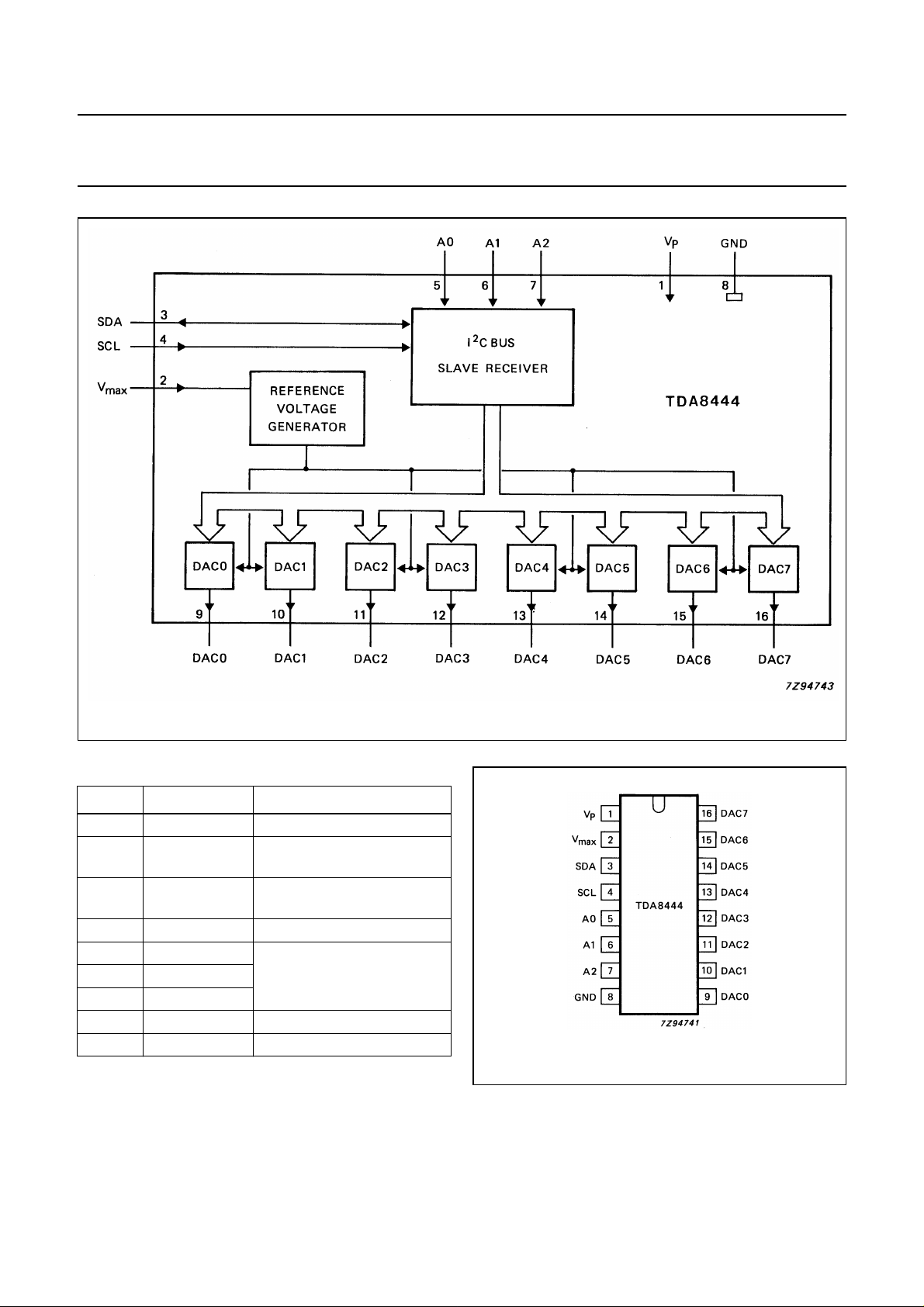
Fig.1 Block diagram.
PINNING
PIN SYMBOL DESCRIPTION
1V
2V
3 SDA I
4 SCL I
5A0
6A1
7A2
8 GND ground
9-16 DAC0-7 analogue voltage outputs
P
max
positive supply voltage
control input for DAC
maximum output voltage
2
C-bus serial data
input/output
2
C-bus serial data clock
programmable address bits
2
C-bus slave receiver
for I
Fig.2 Pinning diagram
March 1991 3
Page 4

Philips Semiconductors Product specification
Octuple 6-bit DAC with I2C-bus
FUNCTIONAL DESCRIPTION
2
I
C-bus
The TDA8444 I2C-bus interface is a receive-only slave. Data is accepted from the I2C-bus in the following format:
S0100A2A1A00AI3I2I1I0SDSCSBSAAXXD5D4D3D2D1D0AP
<----- address byte ----> <----- instruction byte ----> <----- first data byte ---->
Where:
S = start condition A2, A1, A0 = programmable address bits
P = stop condition I3, I2, I1, I0 = instruction bits
A = acknowledge SD, SC, SB, SA = subaddress bits
X = don’t care D5, D4, D3, D2, D1, D0 = data bits
Fig.3 Data format.
Address byte
Valid addresses are 40, 42, 44, 46, 48, 4A, 4C, 4E (hexadec), depending on the programming of bits A2, A1 and A0.
With these addresses, up to eight TDA8444 ICs can be operated independently from one I
are acknowledged by the TDA8444.
2
C-bus. No other addresses
TDA8444
Instruction and data bytes
Valid instructions are 00 to 0F and F0 to FF (hexadec); the TDA8444 will not respond to other instruction values.
Instructions 00 to 0F cause auto-incrementing of the subaddress (bits SD to SA) when more than one data byte is sent
within one transmission. With auto-incrementing, the first data byte is written into the DAC addressed by bits SD to SA
and then the subaddress is automatically incremented by one position for the next data byte in the series.
Auto-incrementation does not occur with instructions F0 to FF. Other than auto-incrementation there is no difference
between instructions 00 to 0F and F0 to FF. When only one data byte per transmission is present, the DAC addressed
by the subaddress will always receive the data.
Valid subaddresses (bits SD to SA) are 0 to 7 (hexadec) relating numerically to DAC0 to DAC7. When the
auto-incrementing function is used, the subaddress will sequence through all possible values (0 to F, 0 to F, etc.).
2
I
C-bus
Input SCL (pin 3) and input/output SDA (pin 4) conform to I2C-bus specifications. Pins 3 and 4 are protected against
positive voltage pulses by internal zener diodes connected to the ground plane and therefore the normal bus line voltage
should not exceed 5.5 V.
The address inputs A0, A1, A2 are programmed by a connection to GND for An = 0 or to VP for An = 1. If the inputs are
left floating, An = 1 will result.
March 1991 4
Page 5

Philips Semiconductors Product specification
Octuple 6-bit DAC with I2C-bus
Input V
Input V
voltage is restricted to approximately V
max
(pin 2) provides a means of compressing the output voltage swing of the DACs. The maximum DAC output
max
while the 6-bit resolution is maintained, so giving a finer voltage resolution of
max
TDA8444
smaller output swings.
Digital-to-analogue converters
Each DAC comprises a 6-bit data latch, current switches and an output driver. Current sources with values weighted by
0
2
up to 25 are switched according to the data input so that the sum of the selected currents gives the required analogue
voltage from the output driver. The range of the output voltage is approximately 0.5 to 10.5 V when V
max
= VP.
The DAC outputs are protected against short-circuits to VP and GND.
To avoid the possibility of oscillations, capacitive loading at the DAC outputs should not exceed 2 nF.
RATINGS
Limiting values in accordance with the Absolute Maximum System (IEC 134)
PARAMETER SYMBOL MIN. MAX. UNIT
Supply voltage V
Supply current (source) I
I2C-bus line voltage V
Input voltage V
Output voltage V
Maximum current on any pin (except pins 1 and 8) ±I
Total power dissipation P
Operating ambient temperature range T
Storage temperature range T
I
P
P
= V
P
= I
= I
3,4
I
O
max
tot
amb
stg
1
1
I
−0.5 18 V
−−10 mA
− 40 mA
−0.5 5.9 V
−0.5 VP+ 0.5 V
−0.5 VP+ 0.5 V
− 10 mA
− 500 mW
−20 +70 °C
−55 +150 °C
THERMAL RESISTANCE
From junction to ambient R
March 1991 5
th j-a
75 K/W
Page 6

Philips Semiconductors Product specification
Octuple 6-bit DAC with I2C-bus
CHARACTERISTICS
All voltages are with respect to GND; T
PARAMETER CONDITIONS SYMBOL MIN. TYP. MAX. UNIT
Supply voltage V
Voltage level for power-on
reset
Supply current no loads; V
all data = 00
Total power dissipation no loads; V
all data = 00
Effective range of
input (pin 2)
V
max
Pin 2 current V
VP = 12 V V
= 1 V I
2
V
= VP I
2
SDA, SCL inputs (pins 3 and 4)
Input voltage range V
Input voltage LOW V
Input voltage HIGH V
Input current LOW V
Input current HIGH V
3;4
3;4
SDA output (pin 3)
Output voltage LOW I
= 3 mA V
3
Sink current I
Address inputs (pins 5 to 7)
Input voltage range V
Input voltage LOW V
Input voltage HIGH V
Input current LOW I
Input current HIGH I
=25°C; VP = 12 V unless otherwise specified
amb
= VP;
max
= VP;
max
= 0.3 V I
= 6 V I
P
V
1
IP = I
P
tot
max
2
2
I
IL
IH
IL
IH
OL
OL
I
IL
IH
IL
IH
1
= V
TDA8444
10.8 12.0 13.2 V
1 − 4.8 V
8 1215mA
− 150 − mW
1.0 − 10.5 V
2
−−−10 µA
−−10 µA
0 − 5.5 V
−−1.5 V
3.0 −−V
−−−10 µA
−−±10 µA
−−0.4 V
38−mA
05V
−−1V
2.1 −−V
−−7−12 µA
−−1µA
March 1991 6
Page 7

Philips Semiconductors Product specification
Octuple 6-bit DAC with I2C-bus
PARAMETER CONDITIONS SYMBOL MIN. TYP. MAX. UNIT
DAC outputs (pins 9 to 16)
Output voltage range V
Minimum output voltage data = 00; I
Maximum output voltage data = 3F; I
at Vmax = VP V
at 1 < Vmax < 10.5 V V
Output sink current V = V
Output source current V = 0 V; data = 1F I
Output impedance data = 1F;
-2 < I
O
Step value of 1 LSB V
Deviation from linearity I
Deviation from linearity I
= VP; IO = -2 mA V
max
= -2 mA; N ≠ 32 0 − 50 mV
O
= -2 mA; N = 32 0 − 70 mV
O
Note to the Characteristics
1. VO = 0.95 V
max
+ V
Omin
.
= −2 mA VOmin 0.1 0.4 0.8 V
O
= −2 mA
O
; data = 1F I
P
< +2 mA
O
O
Z
O
O
Omax
Omax
LSB
TDA8444
0.1 − VP− 0.5 V
10 10.5 11.5 V
see note 1 V
2 8 15 mA
−2 −−6mA
− 450Ω
70 160 250 mV
March 1991 7
Page 8

Philips Semiconductors Product specification
Octuple 6-bit DAC with I2C-bus
APPLICATION INFORMATION
TDA8444
Fig.4 Graph showing output voltage as a function of the input data value for V
VP = 12 V.
March 1991 8
values of 1, 6, 10 and 12 V;
max
Page 9

Philips Semiconductors Product specification
Octuple 6-bit DAC with I2C-bus
PACKAGE OUTLINE
DIP16: plastic dual in-line package; 16 leads (300 mil); long body
D
seating plane
L
Z
16
e
b
b
1
9
A
1
w M
TDA8444
SOT38-1
M
E
A
2
A
c
(e )
1
M
H
pin 1 index
1
0 5 10 mm
DIMENSIONS (inch dimensions are derived from the original mm dimensions)
A
UNIT
mm
inches
Note
1. Plastic or metal protrusions of 0.25 mm maximum per side are not included.
A
max.
4.7 0.51 3.7
OUTLINE
VERSION
SOT38-1
min.
A
1 2
max.
0.15
IEC JEDEC EIAJ
050G09 MO-001AE
b
1.40
1.14
0.055
0.045
b
1
0.53
0.38
0.021
0.015
REFERENCES
cEe M
0.32
0.23
0.013
0.009
D
21.8
21.4
0.86
0.84
8
scale
(1) (1)
6.48
6.20
0.26
0.24
E
(1)
Z
e
0.30
1
0.15
0.13
M
L
3.9
3.4
E
8.25
7.80
0.32
0.31
EUROPEAN
PROJECTION
9.5
8.3
0.37
0.33
w
H
0.2542.54 7.62
0.010.100.0200.19
ISSUE DATE
92-10-02
95-01-19
max.
2.2
0.087
March 1991 9
Page 10

Philips Semiconductors Product specification
Octuple 6-bit DAC with I2C-bus
SOLDERING
Introduction
There is no soldering method that is ideal for all IC
packages. Wave soldering is often preferred when
through-hole and surface mounted components are mixed
on one printed-circuit board. However, wave soldering is
not always suitable for surface mounted ICs, or for
printed-circuits with high population densities. In these
situations reflow soldering is often used.
This text gives a very brief insight to a complex technology.
A more in-depth account of soldering ICs can be found in
“IC Package Databook”
our
Soldering by dipping or by wave
The maximum permissible temperature of the solder is
260 °C; solder at this temperature must not be in contact
DEFINITIONS
(order code 9398 652 90011).
TDA8444
with the joint for more than 5 seconds. The total contact
time of successive solder waves must not exceed
5 seconds.
The device may be mounted up to the seating plane, but
the temperature of the plastic body must not exceed the
specified maximum storage temperature (T
printed-circuit board has been pre-heated, forced cooling
may be necessary immediately after soldering to keep the
temperature within the permissible limit.
Repairing soldered joints
Apply a low voltage soldering iron (less than 24 V) to the
lead(s) of the package, below the seating plane or not
more than 2 mm above it. If the temperature of the
soldering iron bit is less than 300 °C it may remain in
contact for up to 10 seconds. If the bit temperature is
between 300 and 400 °C, contact may be up to 5 seconds.
stg max
). If the
Data sheet status
Objective specification This data sheet contains target or goal specifications for product development.
Preliminary specification This data sheet contains preliminary data; supplementary data may be published later.
Product specification This data sheet contains final product specifications.
Limiting values
Limiting values given are in accordance with the Absolute Maximum Rating System (IEC 134). Stress above one or
more of the limiting values may cause permanent damage to the device. These are stress ratings only and operation
of the device at these or at any other conditions above those given in the Characteristics sections of the specification
is not implied. Exposure to limiting values for extended periods may affect device reliability.
Application information
Where application information is given, it is advisory and does not form part of the specification.
LIFE SUPPORT APPLICATIONS
These products are not designed for use in life support appliances, devices, or systems where malfunction of these
products can reasonably be expected to result in personal injury. Philips customers using or selling these products for
use in such applications do so at their own risk and agree to fully indemnify Philips for any damages resulting from such
improper use or sale.
PURCHASE OF PHILIPS I
2
C COMPONENTS
Purchase of Philips I
components in the I2C system provided the system conforms to the I2C specification defined by
Philips. This specification can be ordered using the code 9398 393 40011.
March 1991 10
2
C components conveys a license under the Philips’ I2C patent to use the
 Loading...