

Page 1

INTEGRATED CIRCUITS
DATA SH EET
TDA8395
SECAM decoder
Preliminary specification
File under Integrated Circuits, IC02
October 1991
Page 2

Philips Semiconductors Preliminary specification
SECAM decoder TDA8395
FEATURES
• Fully integrated filters
• Alignment free
• For use with baseband delay
GENERAL DESCRIPTION
The TDA8395 is a self-calibrating, fully integrated SECAM decoder. The IC should preferably be used in conjunction with
the PAL/NTSC decoder TDA8362 or TDA8366 and with the switched capacitor baseband delay circuit TDA4660. The IC
incorporates HF and LF filters, a demodulator and an identification circuit (luminance is not processed in this IC). The IC
needs no adjustments and very few external components are required. A highly stable reference frequency is required
for calibration and a two-level sandcastle pulse for blanking and burst gating.
QUICK REFERENCE DATA
SYMBOL PARAMETER MIN. TYP. MAX. UNIT
V
P
P
tot
V
16(p-p)
V
O(p-p)
V
O(p-p)
positive supply voltage; pin 3 7.2 − 8.8 V
total power dissipation −−220 mW
composite video input voltage
− 1.0 1.5 V
(peak-to-peak value); pin 16
−(R−Y) output voltage amplitude
− 1.05 − V
(peak-to-peak value); pin 9
−(B−Y) output voltage amplitude
− 1.33 − V
(peak-to-peak value); pin 10
ORDERING INFORMATION
PACKAGE
EXTENDED TYPE NUMBER
PINS PIN POSITION MATERIAL CODE
TDA8395 16 DIL plastic SOT38GE1
Note
1. SOT38-1; 1996 December 3.
(1)
October 1991 2
Page 3
Philips Semiconductors Preliminary specification
SECAM decoder TDA8395
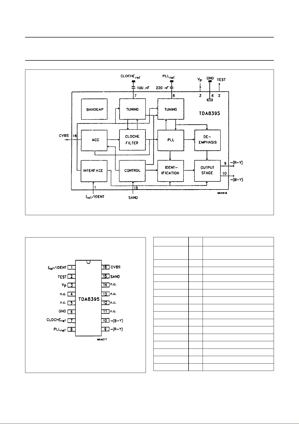
Fig.2 Pin configuration
Fig.1 Block diagram.
PINNING
SYMBOL PIN DESCRIPTION
IDENT 1 reference frequency
f
ref/
TEST 2 test output
V
P
n.c. 4 not connected
n.c. 5 not connected
GND 6 ground
CLOCHE
PLL
ref
−(R−Y) 9 −(R−Y) output
−(B−Y) 10 −(B−Y) output
n.c. 11 not connected
n.c. 12 not connected
n.c. 13 not connected
n.c. 14 not connected
SAND 15 sandcastle pulse input
CVBS 16 video (chrominance) input
ref
input/identification input
3 positive supply voltage
7 Cloche reference filter
8 PLL reference
October 1991 3
Page 4

Philips Semiconductors Preliminary specification
SECAM decoder TDA8395
FUNCTIONAL DESCRIPTION
The TDA8395 is a self-calibrating SECAM decoder
designed for use with a baseband delay circuit.
During frame retrace a 4.433619 MHz reference frequency
is used to calibrate the filters and the demodulator. The
reference frequency should be very stable during this
period.
The Cloche filter is a gyrator-capacitor type filter the
resonance frequency of which is controlled during the
calibration period and offset during scan; this ensures the
correct frequency during calibration.
The demodulator is a Phase-Locked Loop (PLL) type
demodulator which uses the frequency reference and the
bandgap reference to force the PLL to the required
demodulation characteristic.
The low frequency de-emphasis is matched to the PLL and
is controlled by the tuning voltage of the PLL.
A digital identification circuit scans the incoming signal for
SECAM (only line-identification is implemented). The
identification circuit needs to communicate with the
TDA8362 to guarantee that the output signal from the
decoder is only available when no PAL signal has been
identified. If a SECAM signal is decoded a request for
colour-on is transmitted to pin 1 (current is sunk). If the
signal request is granted (i.e. pin 1 is HIGH therefore no
PAL) the colour difference outputs (−(B−Y) and −(R−Y))
from the TDA8362 are high impedance and the output
signals from the TDA8395 are switched ON.
If no SECAM signal is decoded during a two-frame period
the demodulator will be initialized before another attempt
is made also during a two-frame period. The CD outputs
will be blanked or high-impedance depending on the logic
level at pin 1.
A two-level sandcastle pulse generates the required
blanking periods and, also, clocks the digital identification
pulse on the falling edge of the burst gate pulse. To enable
the calibration period to be defined the vertical retrace is
discriminated from the horizontal retrace, this is achieved
by measuring the width of the blanking period.
LIMITING VALUES
In accordance with the Absolute Maximum System (IEC 134)
SYMBOL PARAMETER MIN. MAX. UNIT
V
P
T
stg
T
amb
positive supply voltage − 8.8 V
storage temperature range −25 +150 °C
operating ambient temperature range −25 +70 °C
October 1991 4
Page 5

Philips Semiconductors Preliminary specification
SECAM decoder TDA8395
CHARACTERISTICS
= 8.0 V; T
V
P
SYMBOL PARAMETER CONDITIONS MIN. TYP. MAX. UNIT
Supply (pin 3)
V
P
I
P
P
tot
CVBS input (pin 16)
V
16(p-p)
V
16(p-p)
Z
I
CLOCHE (pin 7)
V
tc
f
0
B bandwidth 241 268 295 kHz
= 25 °C; unless otherwise specified
amb
positive supply voltage 7.2 8.0 8.8 V
supply current − 18 25 mA
total power dissipation − 144 220 mW
composite video input voltage
− 1.0 1.5 V
(peak-to-peak value)
chrominance input voltage
note 1 15 − 300 mV
(peak-to-peak value)
input impedance note 2 − 15 − kΩ
tuning voltage 2.5 3.5 4.5 V
resonance frequency note 3 4.266 4.286 4.306 MHz
Demodulator
V
V
td
O(p-p)
tuning voltage; pin 8 3.5 − 4.8 V
output voltage amplitude
100/75 colour bar 0.97 1.05 1.13 V
(peak-to-peak value); pin 9
V
O(p-p)
output voltage amplitude
100/75 colour bar 1.23 1.33 1.43 V
(peak-to-peak value); pin 10
NLE non-linearity error 100/75 colour bar;
−−3%
note 4
−(B−Y)/−(R−Y) ratio of −(B−Y) and −(R−Y) 1.23 1.27 1.32
f
be−(R−Y)
f
be−(B−Y)
V
O
black-level error −(R−Y) note 5 −−5 kHz
black-level error −(B−Y) note 5 −−7 kHz
output voltage level during
− 2.8 − V
blanking
B
O
output bandwidth − 1.3 − MHz
S/N signal-to-noise ratio note 6 40 −−dB
f
p
pole-frequency LF
77 85 93 kHz
de-emphasis
f
p/f0
ratio of pole and zero
− 3 −
frequency
V
rh(p-p)
residual harmonic voltage
−−10 mV
(peak-to-peak value)
Z
O(e)
output impedance SECAM
pin 1 HIGH −−600 Ω
enabled
Z
O(d)
output impedance SECAM
pin 1 LOW 1 −−MΩ
disabled
October 1991 5
Page 6

Philips Semiconductors Preliminary specification
SECAM decoder TDA8395
SYMBOL PARAMETER CONDITIONS MIN. TYP. MAX. UNIT
Sandcastle pulse
V
bl
V
bg
t
f
Reference/communication
f
ref
V
ref(p-p)
V
ed
V
dd
I
s
blanking detection level 1.0 1.25 1.5 V
burst gate detection level 3.5 3.85 4.2 V
falling edge of burst gate to
8.5 9.0 9.5 µs
start sync
reference frequency note 7 − 4.4336 − MHz
reference voltage amplitude
0.20 − 0.50 V
(peak-to-peak value)
SECAM enable detection
− 2.8 3.3 V
level; pin 1
SECAM disabled detection
note 8 1.5 2.0 − V
level; pin 1
sink current at SECAM
note 9 − 150 −µA
identification; pin 1
Identification
t
i
identification time − 4 − frames
H colour on/off hysteresis 3 −−dB
Notes to the characteristics
1. If measured in the burst-period of a blue line.
2. The video input is AC-coupled.
3. During scan.
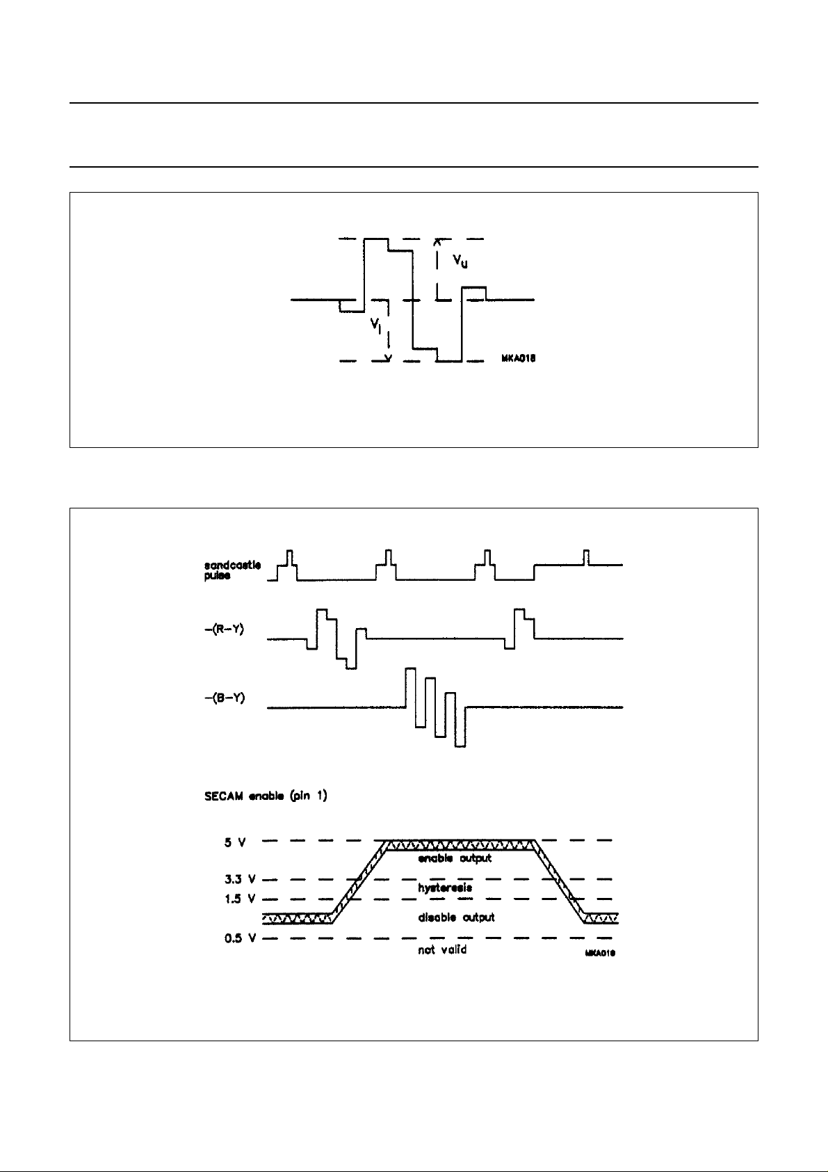
4. Measured as 100% x (IVuI - IVII) / (IVuI + IVlI); see Fig.3.
5. Converted to input frequency error.
6. Defined as the ratio between the peak-to-peak value of the B−Y component of the demodulated 100/75 colour bar
and the peak-to-peak value of the noise.
7. The reference should be stable during frame blanking.
8. The SECAM enable and disable timing should preferably be at the end of the frame blanking.
9. The externally supplied voltage should exceed 0.5 V.
October 1991 6
Page 7
Philips Semiconductors Preliminary specification
SECAM decoder TDA8395
Fig.3 Non-linearity definition.
TIMING
Fig.4 Timing waveforms.
October 1991 7
Page 8

Philips Semiconductors Preliminary specification
SECAM decoder TDA8395
APPLICATION INFORMATION
The leakage current at pin 8 should be well below 20 nA to meet the specification of the black levels (C8 = 220 nF).
The leakage current at pin 7 should be well below 60 nA to meet the specification of the Cloche resonance frequency
(C7 = 100 nF).
The capacitors C7 and C8 should be connected to the ground pin as close as possible to the package. If not, this can
result in a black level error for both channels.
TEST INFORMATION
The performance of the Cloche filter can be measured at pin 2. The use of a FET-probe is advised for low capacitive
loading.
October 1991 8
Page 9
Philips Semiconductors Preliminary specification
SECAM decoder TDA8395
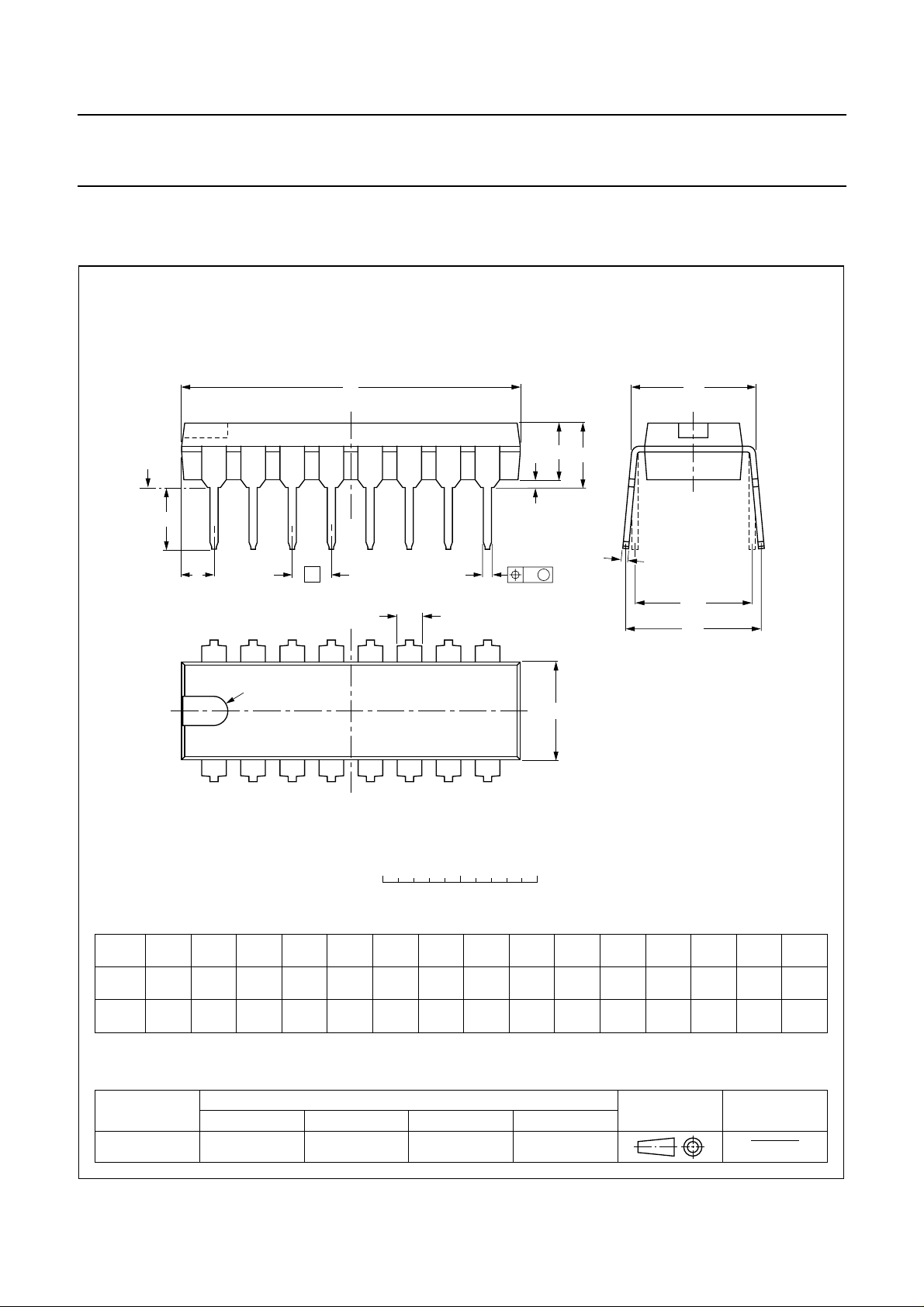
PACKAGE OUTLINE
DIP16: plastic dual in-line package; 16 leads (300 mil); long body
D
seating plane
L
Z
16
pin 1 index
e
b
b
1
9
A
1
w M
SOT38-1
M
E
A
2
A
c
(e )
1
M
H
E
1
0 5 10 mm
scale
DIMENSIONS (inch dimensions are derived from the original mm dimensions)
A
UNIT
mm
inches
Note
1. Plastic or metal protrusions of 0.25 mm maximum per side are not included.
A
max.
4.7 0.51 3.7
OUTLINE
VERSION
SOT38-1
min.
A
1 2
max.
0.15
IEC JEDEC EIAJ
050G09 MO-001AE
b
1.40
1.14
0.055
0.045
b
0.53
0.38
0.021
0.015
1
cEe M
0.32
0.23
0.013
0.009
REFERENCES
(1) (1)
D
21.8
21.4
0.86
0.84
October 1991 9
8
6.48
6.20
0.26
0.24
e
0.30
1
0.15
0.13
M
L
3.9
3.4
E
8.25
7.80
0.32
0.31
EUROPEAN
PROJECTION
H
9.5
0.2542.54 7.62
8.3
0.37
0.010.100.0200.19
0.33
ISSUE DATE
w
92-10-02
95-01-19
Z
max.
2.2
0.087
(1)
Page 10

Philips Semiconductors Preliminary specification
SECAM decoder TDA8395
SOLDERING
Introduction
There is no soldering method that is ideal for all IC packages. Wave soldering is often preferred when through-hole and
surface mounted components are mixed on one printed-circuit board. However, wave soldering is not always suitable for
surface mounted ICs, or for printed-circuits with high population densities. In these situations reflow soldering is often
used.
This text gives a very brief insight to a complex technology. A more in-depth account of soldering ICs can be found in our
“IC Package Databook”
Soldering by dipping or by wave
The maximum permissible temperature of the solder is 260 °C; solder at this temperature must not be in contact with the
joint for more than 5 seconds. The total contact time of successive solder waves must not exceed 5 seconds.
The device may be mounted up to the seating plane, but the temperature of the plastic body must not exceed the
specified maximum storage temperature (T
be necessary immediately after soldering to keep the temperature within the permissible limit.
(order code 9398 652 90011).
). If the printed-circuit board has been pre-heated, forced cooling may
stg max
Repairing soldered joints
Apply a low voltage soldering iron (less than 24 V) to the lead(s) of the package, below the seating plane or not more
than 2 mm above it. If the temperature of the soldering iron bit is less than 300 °C it may remain in contact for up to
10 seconds. If the bit temperature is between 300 and 400 °C, contact may be up to 5 seconds.
DEFINITIONS
Data sheet status
Objective specification This data sheet contains target or goal specifications for product development.
Preliminary specification This data sheet contains preliminary data; supplementary data may be published later.
Product specification This data sheet contains final product specifications.
Limiting values
Limiting values given are in accordance with the Absolute Maximum Rating System (IEC 134). Stress above one or
more of the limiting values may cause permanent damage to the device. These are stress ratings only and operation
of the device at these or at any other conditions above those given in the Characteristics sections of the specification
is not implied. Exposure to limiting values for extended periods may affect device reliability.
Application information
Where application information is given, it is advisory and does not form part of the specification.
LIFE SUPPORT APPLICATIONS
These products are not designed for use in life support appliances, devices, or systems where malfunction of these
products can reasonably be expected to result in personal injury. Philips customers using or selling these products for
use in such applications do so at their own risk and agree to fully indemnify Philips for any damages resulting from such
improper use or sale.
October 1991 10
 Loading...