

Page 1

INTEGRATED CIRCUITS
DATA SH EET
TDA8385
Control circuit for a Self-Oscillating
Power Supply (SOPS)
Preliminary specification
Supersedes data of September 1991
File under Integrated Circuits, IC02
Philips Semiconductors
March 1994
Page 2

Philips Semiconductors Preliminary specification
Control circuit for a Self-Oscillating
Power Supply (SOPS)
FEATURES
• Bandgap reference generator
• Slow-start circuitry
• Low-loss peak current sensing
• Over-voltage protection
• Hysteresis controlled stand-by
function
• Error amplifier with gain setting
• Programmable transfer character
generator
• Protection against open- and
short-circuited feedback loop
ORDERING INFORMATION
EXTENDED TYPE
NUMBER
TDA8385 16 DIL plastic SOT38WBE
PINS PIN POSITION MATERIAL CODE
• Over-load current fold back
characteristic
• LED driver
• Demagnetization protection
• Programmable determination of
switch-on moment of switching
transistor for low-switching losses
• Feed-forward input
• Regulation-indicator output
• Programmable minimum on-time of
switching transistor
• Accurate peak-current setting.
TDA8385
GENERAL DESCRIPTION
The TDA8385 is intended to be used
in combination with the opto-coupler
(CNR50) as a control unit for a
self-oscillating power supply.
PACKAGE
March 1994 2
Page 3

Philips Semiconductors Preliminary specification
Control circuit for a Self-Oscillating
Power Supply (SOPS)
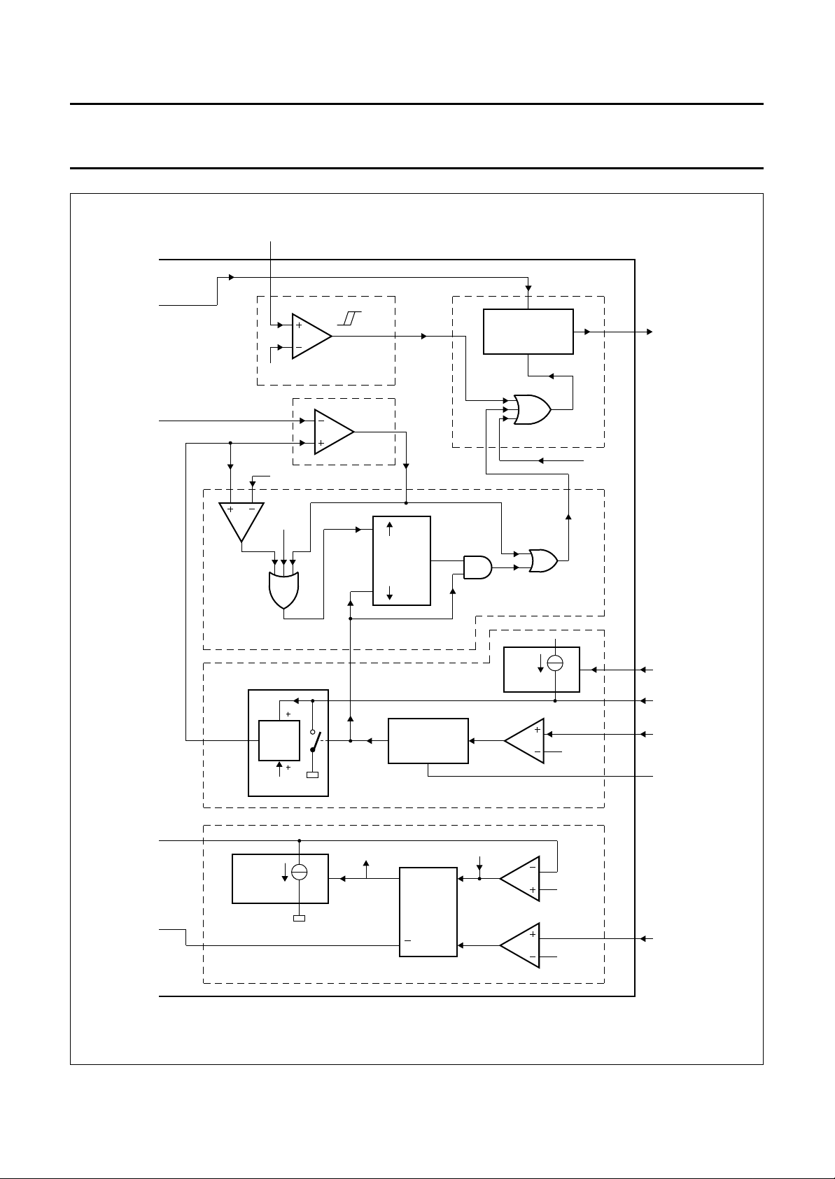
BLOCK DIAGRAMS
handbook, full pagewidth
current reference
setting
feed forward
input
regulation indicator
output
differential amplifier
output
I
ref
3
V
fo
13
1 RIO
11Vdiff
REFERENCE
BLOCK
I
ref
REGULATION
INDICATOR
V
DIFFERENTIAL AMPLIFIER
TDA8385
V
P GND
16 14
latch
V
diff
V
P (min)
DETECTOR
7
V
reset
2812
(28, 27, 23)
mv
V
ts
I
STABILIZED
SUPPLY
V
ref
29
stab
SUPPLY REFERENCES
V
ts
X
V
ref
(2.5 V)
3
feedback voltage
input
transistor-on
setting input
slow start voltage
input
V
9
T
on(min)
4
7Vss
fb
50 µA
5
CLAMP
TCG
2.5 V
4
+
T
V
on (min)
ss
reset (28)
quick
discharge
Fig.1 Block diagram; part A (continued in Fig.2; part B).
V
TCG
CONTROL PART
27
SLOW START
MINIMUM
VOLTAGE
CLAMP
50 µA
charge
19
6
III
VII
MCD417
March 1994 3
Page 4
Philips Semiconductors Preliminary specification
Control circuit for a Self-Oscillating
Power Supply (SOPS)
handbook, full pagewidth
stand-by voltage input
V
10
sb
latch
2.5 V
V
r
V
sim
(28)18
2.5 V
25
STAND-BY
8
2 V
PWM
IV
S
IX
comparator
latch
OUTPUT
STAGE
17
LED DRIVER
TDA8385
LED
15
VI
Q (23)
2
TDA8385
LED driver output
26
demagnetization
100 mV
100 µA
slow
discharge
OVER-VOLTAGE PROTECTION
10
(17) (28)
21
FF
Q
R
13
V
c
DELAY
12
SAWTOOTH GENERATOR
QR
FF
23
S
Q
16
demagnetization
LED CONTROL
I
sim
0.2 I
11
24
22
14
12
I
I
12
9
peak
DEM
115 mV
II
115 mV
over voltage
2.5 V
VIII
V
12
current simulation
input
5
peak-current
setting input
15
demagnetization
input
6
delay setting
8
over-voltage
protection
Fig.2 Block diagram; part B (continued from Fig.1; part A).
March 1994 4
MCD418
Page 5
Philips Semiconductors Preliminary specification
Control circuit for a Self-Oscillating
Power Supply (SOPS)
PINNING
SYMBOL PIN DESCRIPTION
RIO 1 regulation indicator output
LED 2 LED driver output
I
ref
T
on(min)
I
peak
DELAY 6 delay setting
V
ss
OVP 8 over-voltage protection
V
fb
V
sb
V
diff
I
sim
V
fo
GND 14 ground (0 V)
DEM 15 demagnetization input
V
P
3 current reference setting
4 transistor-on setting input
5 peak current setting input
7 slow start voltage input
9 feedback voltage input
10 stand-by voltage input
11 differential amplifier output
12 current simulation input
13 feed forward input
16 positive supply voltage
handbook, 2 columns
T
on(min)
DELAY
I
peak
OVP
RIO
LED
I
V
ref
1
2
3
4
5
6
7
ss
8
Fig.3 Pinning diagram.
TDA8385
TDA8385
MCD402
V
16
P
DEM
15
GND
14
V
13
fo
I
12
sim
V
11
diff
V
10
sb
V
9
fb
FUNCTIONAL DESCRIPTION
The TDA8385 can be divided into
10 functional blocks as shown in Fig.1
and Fig.2.
Block for Figs 1 and 2
BLOCK
NO.
DESCRIPTION
I supply references
II sawtooth generator
III control part
IV pulse width modulator
(PWM)
V LED control
VI LED driver
VII slow-start circuitry
VIII over-voltage protection
IX stand-by circuit
X regulation-indicator
output
These 10 functional blocks of Fig.1
and Fig.2 contain sub-sections
numbered 1 to 28 which are
cross-referenced in the following
description.
Supply references (Block I)
The TDA8385 is intended to be used
on the secondary side of the
self-oscillating power supply. It can be
supplied either by an auxiliary winding
of the transformer or an external
supply e.g. 50 Hz transformer.
Charging of the capacitor C
(see
P
Fig.16) takes place during transistor
on-time (Ton; see Fig.17). During
stand-by the IC is supplied by the
stand-by voltage Vsb (pin 10). The
operating voltage range is from 7.5 to
20 V. The supply current, inclusive
drive current for the LED, is less than
20 mA. A bandgap based reference
(2.5 V) generates a stabilized voltage
V
of 3.9 V to supply all internal
stab
circuits of the IC except the LED
driver. The LED driver is directly
supplied by VP. The reference block
generates all the reference voltages
in the circuit. By means of a resistor
connected to pin 3, a reference
current (I
) is defined.
ref
This current is reflected several times
and is used to obtain IC-independent
settings e.g. T
setting, delay
on(min)
setting, charging and discharging of
slow-start capacitor Css on pin 7
(see Fig.16).
The power supply is released by the
opto-coupler IC at an input voltage
level, which is high enough to
guarantee correct operation of the
TDA8385 e.g. VP = 10 V by sensing
the mains voltage VI. As soon as the
SOPS switching transistor (T1, see
Fig.16) is conductive the capacitor C
is charged. As long as the IC supply
voltage is below 7.5 V the LED driver
is blocked (see latch output;
sub-section 28) in order to guarantee
start-up of SOPS.
During the initialization phase the
quick-discharge-switch
(sub-section 27), set input of
flip-flop (13) and reset input of
flip-flop (23) are also activated.
As soon as the voltage of 7.5 V is
reached the control functions of the IC
are operative. Hysteresis on the
initialization level is 2.3 V.
P
March 1994 5
Page 6
Philips Semiconductors Preliminary specification
Control circuit for a Self-Oscillating
Power Supply (SOPS)
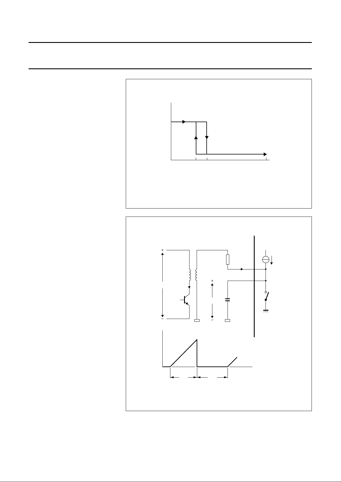
Sawtooth generator (Block II)
URRENT SIMULATION
C
(SEE FIGS 5 AND 16)
The current of the power supply
switching transistor is detected on the
secondary side by an indirect method
of current sensing.
Information of the collector current (Ic)
is obtained by integrating the voltage
of an auxiliary winding of the
transformer during transistor on-time
(Ton). An external capacitor C on pin 5
is charged during Ton by the current
source I
reflection of the current which flows
into pin 12. This current is obtained by
connecting an external resistor R12 to
the auxiliary transformer winding.
During transistor on-time this current
is related to the input voltage VI.
During transistor off time (T
capacitor C is discharged by switch
sw1. This switch is active during the
total T
voltage Vc is formed across C. This
sawtooth is a measure for the
collector current of the switching
transistor T1.
For the voltage Vc yields:
V
c
. The current I
sim
time. In this way a sawtooth
off
I
×
simTon
=
------------------------ C
sim
is the
) the
off
(1)
TDA8385
latch
initialization
operation
5.2 7.5 20
Fig.4 Latch initialization as a function of supply voltage VP.
L
n
n
p
h
V
I
T1
I
c
V
c
R12
C
I
12
VP(V)
12
5
I
sw1
MCD403
sim
I
sim
---------- -
----- n
R12
p
×
p
Where: p = reflection factor;
I
sim
--------I
12
0.2==
p
(2)
V
c
V
n
h
I
×=
(2) → (1) gives:
V
n
p
h
V
c
×
----- -
--- C
n
× T
---------- R12
p
I
×=
on
(3)
March 1994 6
t
T
on
T
off
MCD404
Fig.5 Determination of the peak current Ic.
Page 7

Philips Semiconductors Preliminary specification
Control circuit for a Self-Oscillating
Power Supply (SOPS)
For ‘Ton’ yields:
VcC× np× R12×
T
=
---------------------------------------------- -
on
pn
× V
×
h
I
For the primary current Ic yields:
V
I
T
I
×=
-----
c
on
L
Substitution (4) into (5):
C
I
--- -
c
L
n
1
p
×
× R12× V
-- -
----- -
p
n
h
×=
c
Equation (6) shows that by limiting the
voltage V
the collector peak current
c
can be limited. The peak current is
limited by means of the clamping
circuit in the transfer character
generator (TCG); see Fig.1
sub-section 4.
D
ELAY SETTING (PIN 6)
The output of sub-section 11 is
(4)
extended by the delay circuit of
sub-section 12. The starting
(reference) point of the delay circuit is
the falling edge of the output of
demagnetizing comparator (11) The
(5)
delay can be determined externally by
capacitor (C
The switch-on moment of the
switching transistor can be
(6)
determined by capacitor C
A minimum delay time is required to
prevent transistor T1 from switching
during demagnetization of the
transformer because of oscillations
caused by the leakage inductance.
delay
) on pin 6.
delay
TDA8385
Control part (Block III)
The differential amplifier,
sub-section 3, compares the
feedback voltage (Vfb) with the
reference voltage V
the differential amplifier is available
on pin 11 to allow gain setting. The
differential amplifier is internally
compensated for 0 dB feedback
stability.
The feedback input (pin 9) is also
.
used as the input for the TCG
(see Fig.6) with which a current
foldback characteristic can be
obtained as shown in Fig.7.
. The output of
ref
The clamping level can be externally
influenced by means of a resistor
on pin 7.
The collector peak current can be
influenced in several ways:
• Resistor R12 on pin 12
• Capacitor C on pin 5
• Capacitor on pin 7
• Transfer ratio nh/n
p
• Inductance L
Before comparing the sawtooth
voltage Vc with the control voltage V
in the pulse width modulator, a
voltage of 100 mV is added to Vc. In
this way it will be possible for Vr to
become smaller than V
, which is
sim
important for a stabilized no-load
operation (see Fig.6 area 3).
D
EMAGNETIZATION INPUT (PIN 15)
This input prevents the switching
transistor from conducting during
demagnetization of the transformer in
order to prevent the transformer from
going into saturation. The output of
comparator (11) is HIGH as soon as
the voltage of the transformer winding
exceeds 115 mV.
(3)
V
mv
(4)
(2)
r
(1)
(5)
V
fb
(1), (2), (3) = V
(4), (5) = V
.
TCG
.
diff
V
clamp
V
Ton(min)
MCD405
Fig.6 Reference voltage (Vmv) as a function of feedback voltage (Vfb).
March 1994 7
Page 8
Philips Semiconductors Preliminary specification
Control circuit for a Self-Oscillating
Power Supply (SOPS)
V
O
(5)
(1)
(1), (2), (3) = V
(4), (5) = V
.
TCG
.
diff
Fig.7 Current foldback characteristic; stabilized output voltage (VO)
as function of load current (IO).
(4)
(2)
(3)
I
O
MCD406
TDA8385
The voltage V
minimum on-time of the switching
transistor. This voltage can be
determined externally with a resistor
on pin 4. With this resistor the current
foldback characteristic can be
influenced (see dotted line in Figs 6
and 7).
The minimum on-time is of
importance for the following.
• Stand-by operation
• Starting-up of power supply
• Overload and short-circuit
conditions.
The output of the differential amplifier
(V
), the output of the TCG (V
diff
and the voltage Vss + V
compared in a minimum voltage
clamping circuit (see Fig.1
sub-section 6). The output voltage is
equal to the lowest input voltage.
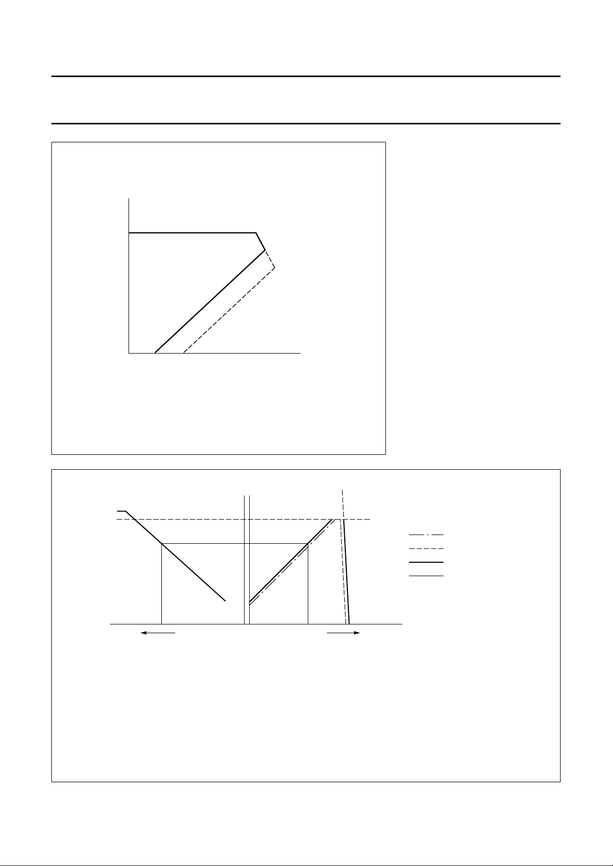
Some relevant characteristics of the
control part are depicted in Fig.8.
Ton(min)
determines the
TCG
are
Ton(min)
)
I
V
c
handbook, full pagewidth
The voltage Vmv determines the collector peak current Ic of transistor T1. The right-hand curve is passed through at start-up. When the feedback voltage
slowly increases from zero, the peak current starts at I
the regulation slope is reached, which is approximately V
The plateau of the top between the points x and y has to be kept as small as possible.
The voltage V
Due to the characteristic of the TCG open- and short-circuit feedback loop will result in low peak current.
An additional signal on pin 13 can be supplied which is subtracted from the signal Vmv. This input can be used for feed forward information.
If no feed forward information is used, pin 13 should be connected to ground.
I
c (max)
I
c (min)
V
+
V
Ton(min)
ss
decreases with the decreasing load. For good no-load operation the peak current has to be made zero with V
diff
mv
xy
and rises along the straight line until I
c(min)
.
ref
V
TCG
V
diff
V
mv
external peak-current
setting (pin 7)
V
ref
V
fb
MCD407
is reached. At a slightly higher feedback voltage
c(max)
.
diff
Fig.8 Characteristics of the control part.
March 1994 8
Page 9

Philips Semiconductors Preliminary specification
Control circuit for a Self-Oscillating
Power Supply (SOPS)
Pulse width modulator (Block IV)
The pulse width modulator compares
the control voltage Vr with the
sawtooth voltage V
sim
. If V
sim
> V
r
output sub-section 8 is HIGH the LED
is switched on and then the switching
transistor is switched off. In this way
the output voltage is controlled.
XAMPLE
E
If the load decreases, VO increases
and therefore Vr decreases. This
causes the LED to start conducting
prematurely, which implies that the
switching transistor is turned off
sooner. The consequence is that the
collector peak current decreases and
hence less energy is stored in the
transformer and VO will decrease.
LED control (Block V)
If either output of sub-section 8 or
output of sub-section 16 are HIGH the
LED is conductive. In order to
improve the start-up behaviour of the
power supply, the demagnetization
signal of sub-section 12 will only
activate the LED driver if flip-flop (13)
has previously been set. The set
signal is generated in the following
three ways.
1. Pulse width modulator
(sub-section 8)
2. Comparator (18)
P(min)
detector
3. V
Set signal (2.) and (3.) are added as
extra security to guarantee a
demagnetization pulse in the event of
the switching transistor not having
enough base current. In that situation
e.g. at start-up, no comparator signal,
set signal (3.) is generated by
sub-section 8.
LED driver (Block VI)
The LED driver (pin 2) is blocked if the
supply voltage VP is in the
initialization phase (see Fig.4). The
output stage is a push-pull stage,
which can sink 5 mA and source
10 mA.
Slow-start circuit (Block VII)
The slow-start circuit is active at
start-up, over voltage protection or
after an overload (short-circuited),
and stand-by mode. The voltage V
and therefore the voltage Vmv and the
peak current Ic slowly increase at
start-up.
By means of sub-section 27 the slow
start voltage Vss is clamped to the
voltage Vfb. If the feedback voltage is
reduced, e.g. as overload, the
slow-start capacitor is discharged to
the level of Vfb. In this way a slow
start-up is also guaranteed after an
overload, short-circuit situation or
after a stand-by mode. The circuit of
sub-section 27 is not active during an
over voltage protection.
When the supply voltage VP is below
the reset-level of 5.2 V
(sub-section 28) the slow-start
capacitor is quickly discharged.
The slow-start input (pin 7) can also
be used for I
connecting a resistor to this pin.
Over voltage protection (Block VIII)
The operation of the over voltage
protection circuit is, in the event of the
IC being SOPS-supplied, quite
different from when the IC is
externally supplied.
c(max)
setting by
TDA8385
O
PERATION WHEN THE IC IS
EXTERNALLY SUPPLIED
When the voltage on pin 8 exceeds
2.5 V the slow-start capacitor is
slowly discharged. During discharge
the LED is permanently conducting.
Discharge is stopped when Vss is
below 115 mV. Flip-flop (23) will then
be reset and the circuit is ready again
for a new slow-start procedure.
During an over voltage sub-section 27
is not active so that the output voltage
VO cannot influence the slow-start
ss
discharge procedure.
PERATION WHEN IC IS
O
SOPS-SUPPLIED (SEE FIGS 9 AND 10)
When the voltage on pin 8 exceeds
2.5 V the slow-start capacitor is
slowly discharged. During discharge
of Css the supply capacitor CP is also
discharged. Because the capacitors
CP and Css have almost the same
value and the supply current I
(≈15 mA) is much larger than the slow
discharge current (≈50 µA), the LED
will be switched off by means of the
V
detection circuit (5.2 V). At that
P(min)
moment the switching transistor will
be switched on again until the 7.5 V
level is reached. During this
hysteresis interval the slow-charge
capacitor is quickly discharged. At the
7.5 V level the LED will be switched
on again because flip-flop (23) output
is still HIGH.
The same procedure will be repeated
several times until the slow-start
capacitor reaches the 115 mV reset
level. At that moment the slow-start
procedure is started again.
If there is still an over voltage the
procedure will be repeated.
Figure 10 is a detailed exposure of
Fig.11.
P
March 1994 9
Page 10

Philips Semiconductors Preliminary specification
Control circuit for a Self-Oscillating
Power Supply (SOPS)
handbook, full pagewidth
(1) For detail see Fig.10.
I
c
V
ss
Fig.9 Over voltage protection.
(1)
TDA8385
t
MCD408
t
Q
V
(V)
V
ss
(V)
I
FF23
P
7.5 V
5.2 V
0
t
slow discharge
quick discharge
0
c
delay
t
t
t
Fig.10 Detailed over voltage protection of Fig.9.
March 1994 10
t
MCD409
Page 11

Philips Semiconductors Preliminary specification
Control circuit for a Self-Oscillating
TDA8385
Power Supply (SOPS)
Stand-by circuit (Block IX)
During stand-by operation the voltage Vsb is supplied from the SOPS via thyristor TH1 (see Fig.16). In the stand-by state,
SOPS operates in a burst mode. When the voltage on pin 10 exceeds 2.5 V the LED driver is permanently activated. The
LED driver is released again if the voltage is below 2 V (see Fig.11).
handbook, full pagewidth
V
sb
(V)
0
2.5 V
2 V
t
output sub-section 25
I
LED
(mA)
0
0
Fig.11 Stand-by operation; burst mode.
t
5 mA
t
MCD410
March 1994 11
Page 12

Philips Semiconductors Preliminary specification
Control circuit for a Self-Oscillating
TDA8385
Power Supply (SOPS)
Regulation indicator output (Block X)
Pin 1 can be used to reset the logic circuit in the TV receiver at power on and off. Sub-section 29 has an open-collector
output. The output of this block is LOW during the regulation mode (V
handbook, full pagewidth
V
2.5
0
V
diff
< Vts; see Fig.12).
diff
V
fb
V
ts
t
V
P
0
V
RIO
0
A desired delay at power-on reset can be made externally.
Fig.12 Regulation indicator output; pin 1.
t
V
: open-collector output
RIO
t
MCD411
March 1994 12
Page 13

Philips Semiconductors Preliminary specification
Control circuit for a Self-Oscillating
TDA8385
Power Supply (SOPS)
LIMITING VALUES
In accordance with the Absolute Maximum Rating System (IEC 134).
All voltages are measured with respect to ground; positive current flow into the IC; all pins not mentioned in the voltage
list are not allowed to be voltage driven. The voltage ratings are valid provided other ratings are not violated; current
ratings are valid provided the power rating is not violated.
SYMBOL PARAMETER CONDITIONS MIN. MAX. UNIT
Voltages
V
P
V
n
V
3
V
8,10
V
12
V
15
Currents
I
1
I
n
I
3
I
5, 6
I
7
I
11
I
16
Temperatures
T
amb
T
stg
Power dissipation
P
tot
supply voltage pin 2 connected −0.5 20 V
pin 2 open-circuit −0.5 18 V
voltage on pins 1, 2, 4, 7, 9 and 13 −0.5 +18 V
voltage on pin 3 −0.5 +6 V
voltage on pins 8 and 10 −0.5 +3.9 V
voltage on pin 12 −0.1 +0.5 V
voltage on pin 15 −0.5 +0.5 V
current on pin 1 0 2 mA
current on pins 2, 12 and 15 −10 +10 mA
current on pin 3 −10mA
current on pins 5 and 6 −1+1mA
current on pin 7 −1 +25 mA
current on pin 11 −10 +0.5 mA
current on pin 16 0 20 mA
operating ambient temperature −25 +70 °C
storage temperature −55 +150 °C
total power dissipation − 500 mW
THERMAL RESISTANCE
SYMBOL PARAMETER THERMAL RESISTANCE
R
th j-a
from junction to ambient in free air 55 K/W
March 1994 13
Page 14

Philips Semiconductors Preliminary specification
Control circuit for a Self-Oscillating
TDA8385
Power Supply (SOPS)
CHARACTERISTICS
= 15 V; I3 = 200 µA; T
V
P
SYMBOL PARAMETER CONDITIONS MIN. TYP. MAX. UNIT
Supply
V
P
V
16
V
16(hys)
I
16
V
11
supply voltage (pin 16) 7.9 − 20 V
supply initialization level 7.1 7.5 7.9 V
internal fixed hysteresis 2.5 − 2.55 V
supply current active LED output −− 20 mA
supply voltage ripple rejection see Figs 13 and 14 − 60 − mV
Reference voltage
V
3
reference voltage at pin 3 0.52 0.55 0.58 V
Error amplifier
V
9
I
9
I
11
I
11
G
o
threshold voltage error amplitude 2.4 2.5 2.6 V
input current feedback input −− 0.5 µA
sink current output V11 = 80 mV 400 −−µA
source current output V11 = 2.5 V 500 −−µA
open loop gain − 100 − dB
B unity gain bandwidth − 600 − kHz
/∆T temperature coefficient −±300 × 10−6− K
∆V
9
V
5
threshold for switching output V
= 25 °C; unless otherwise specified.
amb
= 1.25 V;
diff
V4 = 2 V; V13 = 0 V;
V7> V9; I2 = 2 mA
− V
diff
− V
(1)
− V
os
−1
Transfer characteristic generator
I4/I
V
3
5
current ratio V4 = 0.5 V 0.23 0.25 0.27
threshold for switching output V4 = 0.5 V; V13 = 0 V;
T
on(min)
= 20% V9 = 0.4 V − 0.9 − V
V
fb
= 50% V9 = 1 V 1.4 − V
V
fb
= 80% V9 = 1.6 V − 2.1 − V
V
fb
clamp V
t
PLH
response time pulse width
modulation pin 5 to pin 2
LOW-to-HIGH
t
PHL
response time pulse width
modulation pin 5 to pin 2
HIGH-to-LOW
Feed forward
V
5
threshold for switching output
(Vfo)
I
13
input bias current V13 = 0 V −−1µA
V7> V9; I2 = 2 mA
V9 = 0 V 0.4 − V
= 2.25 V 2.4 − V
9
0.5 − V
os
1.5 − V
os
− 2.6 − V
os
0.6 − V
os
− V
os
1.6 − V
os
− V
os
V
os
V
os
V
os
note 2 −− 700 ns
note 2 −− 1µs
V4 = 0.5 V; V13 = 0 V;
0.6 − V
0.7 − V
os
0.8 − V
os
V
os
V7 = V9 = 3 V;
I2 = 2 mA; V11 = 1 V
March 1994 14
Page 15

Philips Semiconductors Preliminary specification
Control circuit for a Self-Oscillating
TDA8385
Power Supply (SOPS)
SYMBOL PARAMETER CONDITIONS MIN. TYP. MAX. UNIT
Slow-start
I
7/I3
I
7
V
7
V
5
Output stage
V
2(sat)
I
2
V
2
Current simulation
I5/I
12
V
12
V
5(sat)
∆V threshold for switching output;
Demagnetization input
t
demLH
t
demHL
V
15
V
15
C
15
I
15
charge current ratio V7 = 0.5 V 0.22 0.24 0.26
quick discharge current V7 = 1 V 20 −−mA
= 100 mV 50 −−µA
V
7
clamping level I7 = 100 µA 2.8 3.0 3.2 V
threshold for switching output
(Vss)
V4 = 0.5 V; V13 = 0 V;
V7 = 1 V; I2 = 2 mA;
1.4 − V
1.5 − V
os
1.6 − V
os
V
os
V9 = 2 V
saturation voltage I2 = 2 mA −−300 mV
source current V2 = 2 V
operating 4.8 5.3 6.3 mA
initialization phase −−50 µA
open output voltage HIGH I2 = 5 mA 12 −−V
current ratio V5 = 1 V; I12 = 0.5 mA 0.19 0.2 0.21
simulation input voltage I12 = 0.5 mA −− 1.1 V
saturation voltage V15 = V6 = 0 V;
−− 300 mV
I5 = 1 mA
= V6 = 0 V;
V
15
−− 200 mV
I5 = 200 µA
voltage difference between pins 5
and 11; offset simulation voltage
)
(V
os
delay from pin 15 to pin 5
LOW-to-HIGH
delay from pin 15 to pin 5
V4 = 0.5 V; V13 = 0 V;
V7 = V9 = 3 V;
I2 = 2 mA;
V11 = 0.5 V
see Fig.15;
pin 6 not connected
see Fig.15 −− 1µs
60 100 140 mV
−− 500 ns
HIGH-to-LOW
clamping level I15 = 10 mA
positive −− 1.2 V
negative −− −1V
demagnetization threshold
90 115 140 mV
voltage
input capacitance −− 10 pF
input bias current V15 = 60 mV −− 0.5 µA
March 1994 15
Page 16

Philips Semiconductors Preliminary specification
Control circuit for a Self-Oscillating
TDA8385
Power Supply (SOPS)
SYMBOL PARAMETER CONDITIONS MIN. TYP. MAX. UNIT
Delay setting
I
6/I3
I
6
V
6
V
6(sat)
t
dLH
t/c delay setting (t = C
Stand-by
V
10H
V
10(hys)
t
dLH
t
dHL
I
10
Over voltage protection
V
8
t
dLH
t
dHL
V
7
I
7/I3
I
8
Regulation indicator output
V
1
I
1
Notes
1. Vos = V
2. V5 pulse = 1 V; V4 = 0.5 V; V9 = V7= 3 V; V11 = 0.5 V; V13 = 0 V; I2 = 2 mA.
charge current ratio V6 = 1 V 1.1 1.2 1.3
charge current initialization phase V6 = 1 V; V16 = 5 V 2 −−mA
clamping level 2.8 − 3.2 V
saturation voltage V15 = 140 mV − 50 100 mV
delay from pin 6 to pin 2;
V6 crossing the 2.5 V level;
LOW-to-HIGH
C6 = 470 pF;
V5 = 0 V; I2 = 2 mA;
V15 see Fig.15;
−− 1.2 µs
excluding capacitive
tolerances
× V/I) V6 = 2.5 V;
6
− 10 − ns/pF
I3 = 250 µA
threshold level HIGH 2.4 2.5 2.6 V
hysteresis 450 500 550 mV
delay to output pin 10 to pin 2
−− 1µs
LOW-to-HIGH
delay to output pin 10 to pin 2
−− 1µs
HIGH-to-LOW
input current V10 = 2.3 V −− 5µA
threshold level 2.4 2.5 2.6 V
delay to output pin 8 to pin 2
−− 1µs
LOW-to-HIGH
delay to output pin 8 to pin 2
−− 1µs
HIGH-to-LOW
reset level 90 − 140 mV
slow discharge current ratio V7 = 1 V 0.12 0.23 0.31
input current V8 = 3 V −− 1µA
saturation voltage I1 = 1 mA −−300 mV
leakage current V1 = V
offset.
16
−− 1µA
March 1994 16
Page 17

Philips Semiconductors Preliminary specification
Control circuit for a Self-Oscillating
Power Supply (SOPS)
V
P
2 V15 V
t
Frequency = 50 kHz.
Slew rate = 0.2 µs.
Fig.13 Supply voltage ripple rejection;
VP as a function of time.
MCD412
V
diff
(pin 11)
Frequency = 50 kHz.
Slew rate = 0.2 µs.
Fig.14 Supply voltage ripple rejection;
V
as a function of time.
diff
TDA8385
~
3 V
~
MCD413
t
Table 1 Condition of test circuit used for Figs 13 and 14.
PINS STATUS
1, 2, 4 to 6, 12, 13 not connected
8 to 10, 14, 15 ground
3R
7C
16 V
11 V
= 2.7 kΩ
ref
= 4.7 µF
ss
; see Fig.13
P
; see Fig.14
diff
March 1994 17
Page 18

Philips Semiconductors Preliminary specification
Control circuit for a Self-Oscillating
Power Supply (SOPS)
handbook, full pagewidth
demagnetization input
peak-current setting input
(pin 15)
(pin 5)
115 mV
90%
t
demLH demHL
TDA8385
~
+ 0.8 V
~
0 V
~
– 0.8 V
~
1 V
10%
t
0 V
MCD414
Fig.15 Timing diagram; demagnetization delay time.
March 1994 18
Page 19

Philips Semiconductors Preliminary specification
Control circuit for a Self-Oscillating
Power Supply (SOPS)
APPLICATION INFORMATION
O
V
9118
R15
2
1
TDA8385
151016
1/2 CNR50
13
ss
C
delay
C
C
1456 473
12
TDA8385
MCD415
ref
R
Ton(min)
R
o
C
stab
V
f
V
s
n
TH1
p
n
c
I
A
RC
T1
1/2 CNR50
P
V
A
n
P
C
R12
h
handbook, full pagewidth
Fig.16 Application circuit of SOPS with stand-by facility.
I
V
(mains)
March 1994 19
Page 20

Philips Semiconductors Preliminary specification
Control circuit for a Self-Oscillating
Power Supply (SOPS)
V
handbook, full pagewidth
V
f
I
c
O
n
s
V
I
n
p
TDA8385
T
on
storage time and delay
T
off
(SOPS)
output sub-section 11
output sub-section 12
DEMAGNETIZATION
V
c
V
sim
output sub-section 8
COMPARATOR
output sub-section 13
output sub-section 16
DEMAGNETIZATION
output sub-section 14
Q
LED driver
Vr(output sub-section 7)
(output sub-section 10)V
sim
(sub-section 13)
delay
SET
(sub-section 13)
RESET
comparator (18)
level = 1 V
t
MCD416
Fig.17 Application timing diagram.
March 1994 20
Page 21

Philips Semiconductors Preliminary specification
Control circuit for a Self-Oscillating
Power Supply (SOPS)
PACKAGE OUTLINE
22.00
21.35
seating plane
3.9
3.4
2.2
max
2.54
(14x)
1.4 max
0.53
max
1.2 min
0.254
TDA8385
8.25
7.80
5.1
max
M
0.32 max
7.62
9.5
8.3
MSA349
Dimensions in mm.
Fig.18 16-lead dual in-line; plastic with internal heat spreader; opposite bent leads (SOT38WBE).
16
1
9
6.48
6.14
8
March 1994 21
Page 22

Philips Semiconductors Preliminary specification
Control circuit for a Self-Oscillating
TDA8385
Power Supply (SOPS)
SOLDERING
Plastic dual in-line packages
Y DIP OR WAVE
B
The maximum permissible
temperature of the solder is 260 °C;
this temperature must not be in
contact with the joint for more than
5 s. The total contact time of
successive solder waves must not
exceed 5 s.
DEFINITIONS
Data sheet status
Objective specification This data sheet contains target or goal specifications for product development.
Preliminary specification This data sheet contains preliminary data; supplementary data may be published later.
Product specification This data sheet contains final product specifications.
Limiting values
Limiting values given are in accordance with the Absolute Maximum Rating System (IEC 134). Stress above one or
more of the limiting values may cause permanent damage to the device. These are stress ratings only and operation
of the device at these or at any other conditions above those given in the Characteristics sections of the specification
is not implied. Exposure to limiting values for extended periods may affect device reliability.
The device may be mounted up to the
seating plane, but the temperature of
the plastic body must not exceed the
specified storage maximum. If the
printed-circuit board has been
pre-heated, forced cooling may be
necessary immediately after
soldering to keep the temperature
within the permissible limit.
R
EPAIRING SOLDERED JOINTS
Apply a low voltage soldering iron
below the seating plane (or not more
than 2 mm above it). If its temperature
is below 300 °C, it must not be in
contact for more than 10 s; if
between 300 and 400 °C, for not
more than 5 s.
Application information
Where application information is given, it is advisory and does not form part of the specification.
LIFE SUPPORT APPLICATIONS
These products are not designed for use in life support appliances, devices, or systems where malfunction of these
products can reasonably be expected to result in personal injury. Philips customers using or selling these products for
use in such applications do so at their own risk and agree to fully indemnify Philips for any damages resulting from such
improper use or sale.
March 1994 22
Page 23

Philips Semiconductors Preliminary specification
Control circuit for a Self-Oscillating
Power Supply (SOPS)
TDA8385
NOTES
March 1994 23
Page 24

Philips Semiconductors – a worldwide company
Argentina: IEROD, Av. Juramento 1992 - 14.b, (1428)
BUENOS AIRES, Tel. (541)786 7633, Fax. (541)786 9367
Australia: 34 Waterloo Road, NORTH RYDE, NSW 2113,
Tel. (02)805 4455, Fax. (02)805 4466
Austria: Triester Str. 64, A-1101 WIEN, P.O. Box 213,
Tel. (01)60 101-1236, Fax. (01)60 101-1211
Belgium: Postbus 90050, 5600 PB EINDHOVEN, The Netherlands,
Tel. (31)40 783 749, Fax. (31)40 788 399
Brazil: Rua do Rocio 220 - 5
CEP: 04552-903-SÃO PAULO-SP, Brazil.
P.O. Box 7383 (01064-970).
Tel. (011)829-1166, Fax. (011)829-1849
Canada: INTEGRATED CIRCUITS:
Tel. (800)234-7381, Fax. (708)296-8556
DISCRETE SEMICONDUCTORS: 601 Milner Ave,
SCARBOROUGH, ONTARIO, M1B 1M8,
Tel. (0416)292 5161 ext. 2336, Fax. (0416)292 4477
Chile: Av. Santa Maria 0760, SANTIAGO,
Tel. (02)773 816, Fax. (02)777 6730
Colombia: Carrera 21 No. 56-17, BOGOTA, D.E., P.O. Box 77621,
Tel. (571)217 4609, Fax. (01)217 4549
Denmark: Prags Boulevard 80, PB 1919, DK-2300 COPENHAGEN S,
Tel. (032)88 2636, Fax. (031)57 1949
Finland: Sinikalliontie 3, FIN-02630 ESPOO,
Tel. (9)0-50261, Fax. (9)0-520971
France: 4 Rue du Port-aux-Vins, BP317,
92156 SURESNES Cedex,
Tel. (01)4099 6161, Fax. (01)4099 6427
Germany: P.O. Box 10 63 23, 20095 HAMBURG ,
Tel. (040)3296-0, Fax. (040)3296 213
Greece: No. 15, 25th March Street, GR 17778 TAVROS,
Tel. (01)4894 339/4894 911, Fax. (01)4814 240
Hong Kong: 15/F Philips Ind. Bldg., 24-28 Kung Yip St.,
KWAI CHUNG, Tel. (0)4245 121, Fax. (0)4806 960
India: PHILIPS ELECTRONICS & ELECTRICALS Ltd.,
Components Dept., Shivsagar Estate, Block 'A',
Dr. Annie Besant Rd., Worli, BOMBAY 400 018,
Tel. (022)4938 541, Fax. (022)4938 722
Indonesia: Philips House, Jalan H.R. Rasuna Said Kav. 3-4,
P.O. Box 4252, JAKARTA 12950,
Tel. (021)5201 122, Fax. (021)5205 189
Ireland: Newstead, Clonskeagh, DUBLIN 14,
Tel. (01)640 000, Fax. (01)640 200
Italy: Viale F. Testi, 327, 20162 MILANO,
Tel. (02)6752.1, Fax. (02)6752.3350
Japan: Philips Bldg13-37, Kohnan 2-chome, Minato-ku, KOKIO 108,
Tel. (03)3740 5101, Fax. (03)3740 0570
Korea: (Republic of) Philips House, 260-199 Itaewon-dong,
Yongsan-ku, SEOUL, Tel. (02)794-5011, Fax. (02)798-8022
Malaysia: No. 76 Jalan Universiti, 46200 PETALING JAYA,
SELANGOR, Tel. (03)757 5511, Fax. (03)757 4880
Mexico: Philips Components, 5900 Gateway East, Suite 200,
EL PASO, TX 79905, Tel. 9-5(800)234-7381, Fax. (708)296-8556
Netherlands: Postbus 90050, 5600 PB EINDHOVEN,
Tel. (040)78 37 49, Fax. (040)78 83 99
New Zealand: 2 Wagener Place, C.P.O. Box 1041, AUCKLAND,
Tel. (09)849-4160, Fax. (09)849-7811
Norway: Box 1, Manglerud 0612, OSLO,
Tel. (22)74 8000, Fax. (22)74 8341
th
floor, Suite 51,
Pakistan: Philips Markaz, M.A. Jinnah Rd., KARACHI 3,
Tel. (021)577 039, Fax. (021)569 1832
Philippines: PHILIPS SEMICONDUCTORS PHILIPPINES Inc,
106 Valero St. Salcedo Village, P.O. Box 2108 MCC, MAKATI,
Metro MANILA, Tel. (02)810 0161, Fax. (02)817 3474
Portugal: Av. Eng. Duarte Pacheco 6, 1009 LISBOA Codex,
Tel. (01)683 121, Fax. (01)658 013
Singapore: Lorong 1, Toa Payoh, SINGAPORE 1231,
Tel. (65)350 2000, Fax. (65)251 6500
South Africa: 195-215 Main Road, Martindale,
P.O. Box 7430,JOHANNESBURG 2000,
Tel. (011)470-5433, Fax. (011)470-5494
Spain: Balmes 22, 08007 BARCELONA,
Tel. (03)301 6312, Fax. (03)301 42 43
Sweden: Kottbygatan 7, Akalla. S-164 85 STOCKHOLM,
Tel. (0)8-632 2000, Fax. (0)8-632 2745
Switzerland: Allmendstrasse 140, CH-8027 ZÜRICH,
Tel. (01)488 2211, Fax. (01)481 7730
Taiwan: 23-30F, 66, Chung Hsiao West Road, Sec. 1, P.O. Box
22978, TAIPEI 10446, Tel. (2)388 7666, Fax. (2)382 4382
Thailand: PHILIPS ELECTRONICS (THAILAND) Ltd.,
60/14 MOO 11, Bangna - Trad Road Km. 3
Prakanong, BANGKOK 10260,
Tel. (2)399-3280 to 9, (2)398-2083, Fax. (2)398-2080
Turkey: Talatpasa Cad. No. 5, 80640 LEVENT/ISTANBUL,
Tel. (0212)279 2770, Fax. (0212)269 3094
United Kingdom: Philips Semiconductors Limited, P.O. Box 65,
Philips House, Torrington Place, LONDON, WC1E 7HD,
Tel. (071)436 41 44, Fax. (071)323 03 42
United States:INTEGRATED CIRCUITS:
811 East Arques Avenue, SUNNYVALE, CA 94088-3409,
Tel. (800)234-7381, Fax. (708)296-8556
DISCRETE SEMICONDUCTORS: 2001 West Blue Heron Blvd.,
P.O. Box 10330, RIVIERA BEACH, FLORIDA 33404,
Tel. (800)447-3762 and (407)881-3200, Fax. (407)881-3300
Uruguay: Coronel Mora 433, MONTEVIDEO,
Tel. (02)70-4044, Fax. (02)92 0601
For all other countries apply to: Philips Semiconductors,
International Marketing and Sales, Building BAF-1,
P.O. Box 218, 5600 MD, EINDHOVEN, The Netherlands,
Telex 35000 phtcnl, Fax. +31-40-724825
SCD29 © Philips Electronics N.V. 1994
All rights are reserved. Reproduction in whole or in part is prohibited without the
prior written consent of the copyright owner.
The information presented in this document does not form part of any quotation
or contract, is believed to be accurate and reliable and may be changed without
notice. No liability will be accepted by the publisher for any consequence of its
use. Publication thereof does not convey nor imply any license under patent- or
other industrial or intellectual property rights.
Printed in The Netherlands 9397 730 30011
Philips Semiconductors
 Loading...