

Page 1

HORIZONTALANDVERTICALDEFLECTION CIRCUIT
.
DIRECTLINEDARLINGTONDRIVE
.
DIRECTFRAME-YOKEDRIVE (± 1A)
.
COMPOSITEVIDEOSIGNALINPUT
CAPABILITY
.
FRAME OUTPUT PROTECTION AGAINST
SHORT CIRCUITS
.
PLL
.
VIDEOIDENTIFICATION CIRCUIT
.
SUPERSANDCASTLEOUTPUT
.
VERYFEW EXTERNALCOMPONENTS
.
VERYLOW COST POWERPACKAGE
DESCRIPTION
The TDA8215Bisanhorizontalandverticaldeflection circuit with super sandcastle generator and
video identification output. Used with TDA8213
(Video & Sound IF system) and TDA8217 (Pal
decoder and video processor), this IC permits a
complete low-cost solution for PAL applications.
The TDA8215B has been specially designed for
direct drive of line DARLINGTONtransistors.
TDA8215B
POWERDIP 16 + 2 + 2
(Plastic Package)
ORDER CODE : TDA8215B
PINCONNECTIONS
FRAME FLYBACK GENERATOR
POWER AMPLIFIERINPUT
VIDEO IDENTIFICATION OUTPUT
September 1993
CC1
FRAME OSCILLATOR
V
CC2
GROUND
GROUND
FRAME POWER SUPPLY
FRAME OUTPUT LINE OSCILLATOR
1
2
3
4
5
6
7
8
9
10
20
19
18
17
16
15
14
13
12
11
VIDEO INPUTV
SUPER SANDCASTLE OUTPUT
LINE FLYBACK INPUT
LINE OUTPUT
GROUND
GROUND
RC NETWORK
LINE SAWTOOTH INPUT
PHASE DETECTOR
8215B-01.EPS
1/9
Page 2

TDA8215B
BLOCK DIAGRAM
Vcc2
Vcc1
Video
Identification
Video
Input
Line
Flyback
19
20
18
8
2µs
Line flyback
ABSOLUTE MAXIMUM RATINGS
Symbol Parameter Value Unit
1 Supply Voltage 30 V
V
CC
2 Flyback Generator Supply Voltage 35 V
V
CC
V9 Frame Power Supply Voltage 60 V
I10
NR
I10 Frame Output Current (continuous) ±
V17 Line Output Voltage (external) 60 V
17 Line Output Peak Current 0.8 A
I
P
17 Line Output Continuous Current 0.4 A
I
C
T
STG
T
J
T
AMB
Frame Output Current (nonrepetitive) ±
Storage Temperature -40 to + 150
Max Operating Junction Temperature + 150
Operating Ambient Temperature 0 to 70
129
Frame
blanking
detector
Σ
detector
Input
stage
Vcc1
Frame
oscillator
Frame-Synchro
generator
Burst gate pulse
generator
2µs
14
+
Power
-
stage
Phase
detector
13
12
3
4
Flyback
generator
Output
stage
Line
oscillator
11
10
17
YOKE
7
Vcc1
8215B-02.EPS
1.5
1
A
A
o
C
o
C
o
C
8215B-01.TBL
THERMALDATA
Symbol Parameter Value Unit
R
TH(j-c)
R
TH(j-a)
T
J
2/9
Max Junction-case Thermal Resistance 10
Typical Junction-ambient Thermal Resistance
(Soldered on a 35µm thick 45cm2PC Board copperarea)
40
Max Recommended Junction Temperature 120
o
C/W
o
C/W
o
C
8215B-02.TBL
Page 3
TDA8215B
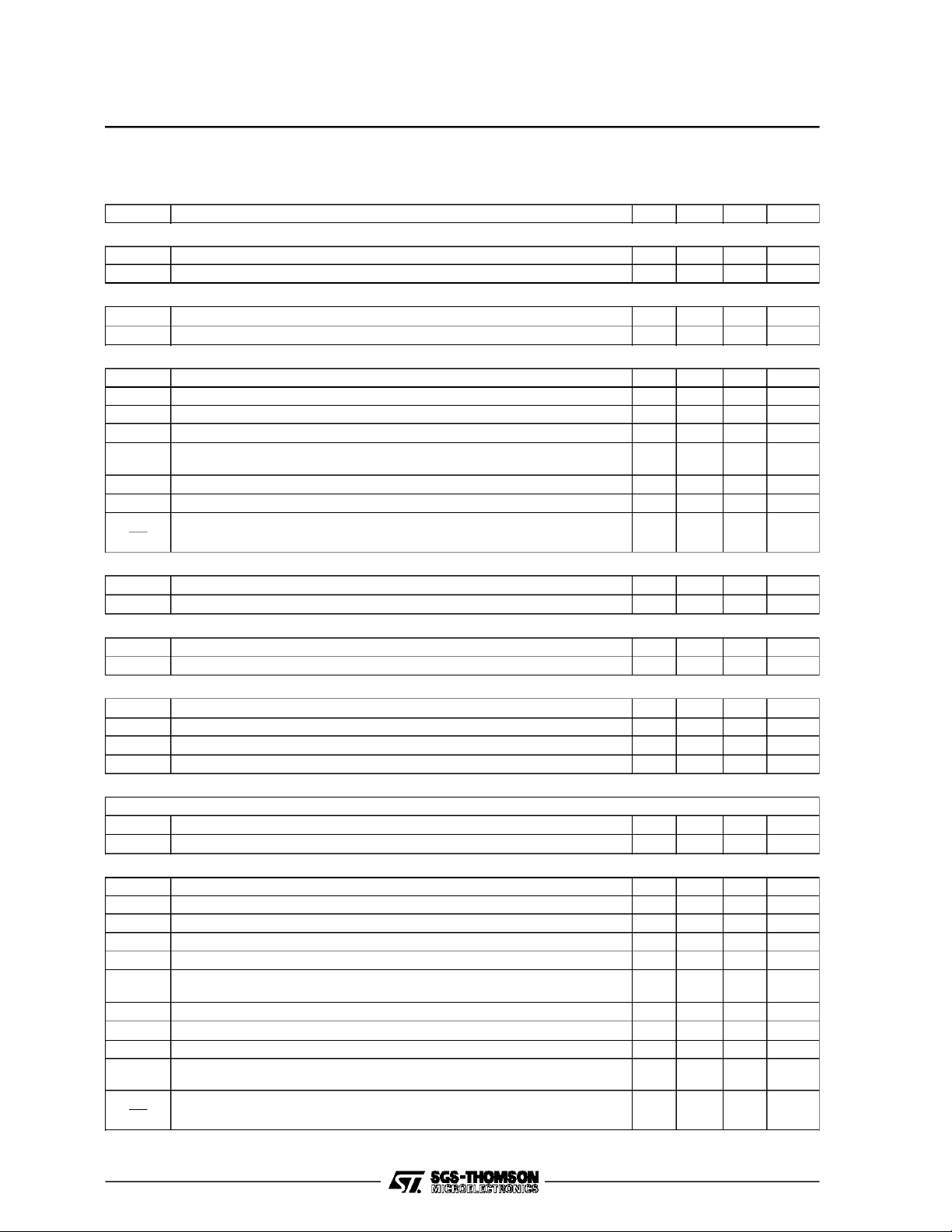
ELECTRICAL CHARACTERISTICS
= 10V,T
V
CC1
Symbol Parameter Min. Typ. Max. Unit
SUPPLY (Pin 1)
Supply Current 15 mA
Supply Voltage 9 10 10.5 V
CC1
V
I
CC1
VIDEO INPUT (Pin 20)
V20
Reference Voltage (I
MWF Minimum Width of Frame Pulse (When synchronized with TTL signal) 50 µ
LINE OSCILLATOR (Pin 11)
LT11 Low Threshold Voltage 2.8 3.2 3.6 V
HT11 High Threshold Voltage 5.4 6.6 7.8 V
BI11 Bias Current 100 nA
DR11 Discharge Impedance 1.0 1.4 1.8
FLP1 Free Running Line Period
(R = 34.9kΩ Tied to V
FLP2
Free Running Line Period (R = 13.7KΩ, C = 2.2nF)
OT11 Oscillator Threshold for Line Output Pulse Triggering 4.6 V
∆F
∆θ
Horizontal Frequency Drift with Temperature (see application) 2 Hz/
LINE OUTPUT (Pin 17)
LV17
OPW
Saturation Voltage (I
Output Pulse width (line period = 64µs , negative pulse)
LINE SAWTOOTH INPUT (Pin 13)
V13 Bias Voltage 1.8 2.4 3.2 V
Z13 Input Impedance 4.5 5.8 8
PHASE DETECTOR (Pin 12)
I12 Output Current During Synchro Pulse 250 350 500 µ
RI12 Current Ratio (positive/negative) 0.95 1 1.05
LI12 Leakage Current -2 +2 µ
CV12 Control VoltageRange 2.60 7.10 V
VIDEO IDENTIFICATION (Pin 8)
Low Level Output when the line synchro tip is centered in the line retrace
V
V
without Video Signal (I8= -500µA)
H8
with Video Signal (I8=50µA)
L8
FRAME OSCILLATOR (Pin 2)
LT2 Low Threshold Voltage 1.6 2.0 2.3 V
HT2 High Threshold Voltage 2.6 3.1 3.6 V
DIF2 LT2 - HT2 1.0 V
BI2 Bias Current 30 nA
DR2 Discharge Impedance 300 470 700 Ω
FFP1 Free Running Frame Period
(R = 845kΩ Tied to V
MFP
FFP2
Minimum Frame Period (I
Free Running Frame Period (R = 408kΩ, C = 220nF)
FPR Frame Period Ratio = FFP/MFP 1.7 1.8 1.9
FG Frame Saw-tooth Gain Between Pin 1 and non Inverting Input of the Frame
Amplifier
∆F
∆θ
Vertical Frequency Drift with Temperature (see application) 4.10
=25oC (unless otherwisespecified )
AMB
=-1µA)
20
, C = 2.2nF Tied to Ground)
CC1
= 800mA during 2µs)
17
, C = 180nF Tied to Ground)
CC1
= -100µA) with the Same RC
20
1.4 1.75 2 V
62 64 66 µ
27 µ
2.2 V
19 21 23
4.5 6.3 0.9 V
0.6 0.9 V
20.5 23 25 ms
12.8 ms
14.3 ms
-0.4
-3
s
kΩ
s
s
o
µs
kΩ
A
A
Hz/oC
C
8215B-03.TBL
3/9
Page 4

TDA8215B
ELECTRICAL CHARACTERISTICS (continued)
=10V,T
V
CC1
Symbol Parameter Min. Typ. Max. Unit
FRAME POWER SUPPLY (Pin 9)
V9 Operating Voltage (with flyback Generator) 10 58 V
I9 Supply Current (V9 = 30V) 11 22 mA
FLYBACK GENERATOR SUPPLY (Pin 3)
V
2 Operating Voltage 10 30 V
CC
FRAME OUTPUT (Pin 10)
Saturation Voltage to Ground (V9 = 30V)
LV10A I10 = 0.1A 0.06 0.6 V
LV10B I10 = 1A 0.37 1 V
Saturation Voltage to V9 (V9 = 30V)
HV10A I10 = -0.1A 1.3 1.6 V
HV10B I10 = -1A 1.7 2.4 V
Saturation Votage to V9 in Flyback Mode (V10 > V9)
FV10A I10 = 0.1A 1.6 2.1 V
FV10B I10 = 1A 2.5 4.5 V
FLYBACK GENERATOR (Pin 3 and Pin 4)
Flyback Transistoron (output = high state), V
F2DA I
F2DB I
Flyback Transistoron (output = high state), V
FSVA I
FSVB I
Flyback Transistoroff (output = V9 - 8V), V9 - V
FCI Leakage Current Pin 3 170 µ
SUPER SANDCASTLE OUTPUT (Pin 19)
Output Voltages (R load = 2.2kΩ)
SANDT2 Frame blanking pulse level 2 2.5 3 V
SANDL2 Line blanking pulse level 4 4.5 5 V
BG2 Burst key pulse level 8 9 V
Pulses width and timing
SC3 Delay between middle of sync pulse and leading edge of burst key pulse 2.3 2.7 3.1 µ
SC2 Duration of burst key pulse
Vertical blanking pulse width
LINE FLYBACK INPUT (Pin 18)
Switching level 2 V
Maximum imput current at V
Limiting voltage at maximum current 4.3 V
τ RC network time constant (Note 2) 6 µs
Notes : 1. Width of vertical blanking pulseon SSC output is proportional to the frame flyback time, the switching level is VCC2-2VBEand
the other input of the comparator is tied to the frame amplifier output. Application circuit uses the frame flyback generator.
2. An RC network is connected to this input. Typical value for the resistor is27kΩ and 220pF for the capacitor. A different time
constant forRC changes the delaybetween the middle of the line synchro pulse and theleading edge of the burst key pulse but
also the duration of the burst keypulse.
=25oC (unless otherwisespecified )
AMB
= 30V, V4/3 with
CC2
= 0.1A 1.5 2.1 V
4 → 3
=1A 3.0 4.5 V
4 → 3
= 30V, V3/4 with
CC2
= 0.1A 0.8 1.1 V
3 → 4
=1A 2.2 4.5 V
3 → 4
= 30V
CC2
3.7 4
Note1
= 800V 8 mA
PEAK
5
µs
A
s
8215B-04.TBL
4/9
Page 5

TDA8215B
GENERALDESCRIPTION
The TDA8215B performs all the video and power
functions required to provide signals for the line
driverand frame yoke.
It contains:
- A synchronizationseparator
- An integrated frame separator without external
components
- A saw-tooth generator for the frame
- A power amplifier for direct drive of frame yoke
(short circuitprotected)
- An open collector output for the line darlington
drive
Figure 1 : SynchronizationSeparatorCircuit
VR
Video
R1
- Aline phasedetector and a voltage controloscillator
- Asuper sandcastlegenerator
- Video identificationoutput.
The slice level of sync-separationis fixedby value
of the external resistors R1 and R2. VR is an
internallyfixed voltage.
The sync-pulseallows the dischargeof the capacitor by a 2 x I current.A line sync-pulseis not able
to discharge the capacitor under V
/2. A frame
Z
sync-pulse permits the complete discharge of the
capacitor, so during the frame sync-pulse Q
providecurrentfor the other parts of thecircuit.
Q
4
SL2SL1
20
3
and
Figure 2 : FrameSeparator
SL1
R2
8215B-03.EPS
Vz
Q3
I
3I
ST1
/2
Vz
Q4
ST2
8215B-04.EPS
5/9
Page 6

TDA8215B
Figure 3 : LineOscillator
Vcc1
R5
11
Phase
comparator
output
R4
The oscillator thresholds are internally fixed by
resistors. The discharge of the capacitordepends
on the internal resistor R4. The control voltage is
appliedon resistorR5.
Figure 4 : PhaseComparator
Line
Flyback
8215B-05.EPS
comparatorisan alternativelynegativeandpositive
current.The frame sync-pulseinhibits the comparatorto preventfrequency drift of the lineoscillator
on the frame beginning.
Figure5
Vcc1
12
13
Integrated
Flyback
Sync pulse
Output
Current
Vc
The sync-pulsedrives the current in the comparator.The line flyback integrated by the external net
workgives on pin 13 a saw tooth, the DC offset of
this saw tooth is fixed by VC. The comparator
outputprovidesa positivecurrent forthe partof the
signalon pin13 greater than to VC and a negative
currentfor theotherpart.Whenthe lineflybackand
thevideosignal aresynchronized,theoutputofthe
6/9
SL2
ST1
8215B-06.EPS
Line output (Pin 17)
It is an open-collectoroutput. The output negative
pulse time is 22µs fora 64µs period.
The oscillator thresholds are internally fixed by
resistors.Theoscillatoris synchronized duringthe
last half free run period. The input current during
the charge of thecapacitoris less than 100nA.
Vc
8215B-07.EPS
Page 7

Figure 6 : FrameOscillator
INPUTCURRENT
COMPENSATION
2
TDA8215B
Vcc1
Frame
sync pulse
To frame amplifier
Frame output amplifier
This amplifier is able to drive directly the frame
yoke. Its output is short circuit and overload protected;it contains also a thermalprotection.
Theframeblankingisdetectedbythe frameflyback
generator. When the output voltage of the frame
amplifier exceeds V
2-2VBE, the pulse is de-
CC
tected.The line flyback detection is provided by a
comparatorwhich comparesthe input line flyback
pulseto aninternalreference.Theburst gatepulse
position is fixed by the external RC network
(Pin 14). It is referenced to the middle of the line
Figure 7 : SuperSandcastleGenerator
Line
Flyback
Vcc1
Input
18
Frame
Output
10
YOKE
Line
Flyback
Detection
Frame
Blanking
Detection
flyback.
This stage will detect thecoincidencebetween the
line sync pulse (if present) and a 2µs sampling
pulse. This 2µs pulse is positionned at the center
of line sync pulse when the phase loop is locked.
This sampled detection is stored by an external
capacitor Pin 8.
The identification output level is high when video
signalis present.
Important remark : minimum saw-tooth amplitude
on Pin13 has to be 2V
Σ
Burst gate
pulse
generator
RC
400µ A
(typ.: 2.5VPP).
PP
Vcc1
19
SSC
Output
8215B-08.EPS
RC
Network
14
8215B-09.EPS
7/9
Page 8

TDA8215B
Figure 8 : VideoIdentificationCircuit(Pin 8)
V
13
H
2.75V
V
L
2.25V
5.8kΩ
V
CC1
Line retrace
V
R
2.5V
V
CC1
12µs
Line
Flyback
Integrated
Flyback
V
H
V
L
V
R
10kΩ
Video
Ident.
Output
1N4148
BC547
10µF
TYPICALAPPLICATION
Vcc
+24V
Video
Input
Vcc1
Line
Flyback
100µF
27kΩ
220pF 180nF
220nF
1.5kΩ
120pF
560kΩ
15kΩ
68pF
100kΩ
180pF
4.7Ω
100nF
22nF
22nF
4.7kΩ
1µF
SamplingPulse
1kΩ
V
R1
8
Line Sync.
100nF
820kΩ
218394
14
20
10µF
10kΩ
IN4148
470µF
Vcc1
IN4002
BC547
47µF
TDA 8215B
13
18
12 11 5 6 15 16 19 17
100kΩ
12nF
2.2nF
22kΩ
Vcc1
22kΩ
Horizontal
Frequency
SSC
2.2kΩ
Line
Sync.
V
R1
Video Identification
IN4148
10
7
220kΩ 220kΩ
680pF
22kΩ
Vertical
100Ω
Amplitude
Vcc1
10µF
Line Yoke
193mH, 22Ω, Ipp = 4A
Line Darlington
SGSD00055
I8
220nF
100nF
Frame Yoke
30 mH, 15Ω
I = 840mA
pp
100Ω
withvideo
withoutvideo
8215B-10.EPS
2.2Ω
270Ω
1000µF
1Ω
8215B-11.EPS
8/9
Page 9

PACKAGE MECHANICAL DATA
20 PINS - PLASTICPOWERDIP
TDA8215B
I
a1
b1
E
Z
Dimensions
L
b
e3
20 11
110
B
D
e
Z
F
Millimeters Inches
Min. Typ. Max. Min. Typ. Max.
a1 0.51 0.020
B 0.85 1.4 0.033 0.055
b 0.5 0.020
b1 0.38 0.5 0.015 0.020
D 24.8 0.976
E 8.8 0.346
e 2.54 0.100
e3 22.86 0.900
F 7.1 0.280
i 5.1 0.201
L 3.3 0.130
Z 1.27 0.050
Information furnished is believed to be accurate and reliable. However, SGS-THOMSON Microelectronics assumes no responsibility
for the consequences of use of such information norfor any infringement of patents or otherrights of third partieswhich may result
from itsuse. No licence is granted by implication or otherwise under any patent or patent rights of SGS-THOMSON Microelectronics.
Specifications mentioned in this publication are subject to change without notice. This publication supersedes and replaces all
information previously supplied. SGS-THOMSON Microelectronics products are not authorized for use as critical components in life
support devices or systems without express written approval of SGS-THOMSON Microelectronics.
PMDIP20W.EPS
DIP20PW.TBL
1994 SGS-THOMSON Microelectronics - All Rights Reserved
Purchase of I
2
I
C Patent. Rights touse these components in a I2C system, is granted provided that the system conforms to
Australia - Brazil - China - France - Germany - Hong Kong - Italy -Japan - Korea - Malaysia - Malta - Morocco
The Netherlands - Singapore - Spain - Sweden - Switzerland - Taiwan - Thailand - United Kingdom - U.S.A.
2
C Components of SGS-THOMSON Microelectronics, conveys a license under the Philips
2
the I
C Standard Specifications as definedby Philips.
SGS-THOMSON Microelectronics GROUP OFCOMPANIES
9/9
 Loading...