

Page 1

TV VERTICALDEFLECTIONBOOSTER
.
POWERAMPLIFIER
.
FLYBACKGENERATOR
.
THERMAL PROTECTION
DESCRIPTION
Designedfor monitorsand high performanceTVs,
the TDA8179Svertical deflectionbooster delivers
flybackvoltagesup to 90V.
The TDA8179S operates with supplies up to 42V
and provides up to 2App output current to drive to
yoke.
The TDA8179S is offered in HEPTAWATT package.
TDA8179S
HEPTAWATT
(Plastic Package)
ORDER CODE : TDA8179S
PIN CONNECTIONS
Tab connectedto pin 4
May 1993
7
6
5
4
3
2
1
Non-invertingInput
Output Stage Supply
Output
GND
Flyback Generator
SupplyVoltage
InvertingInput
8179S-01.EPS
1/6
Page 2
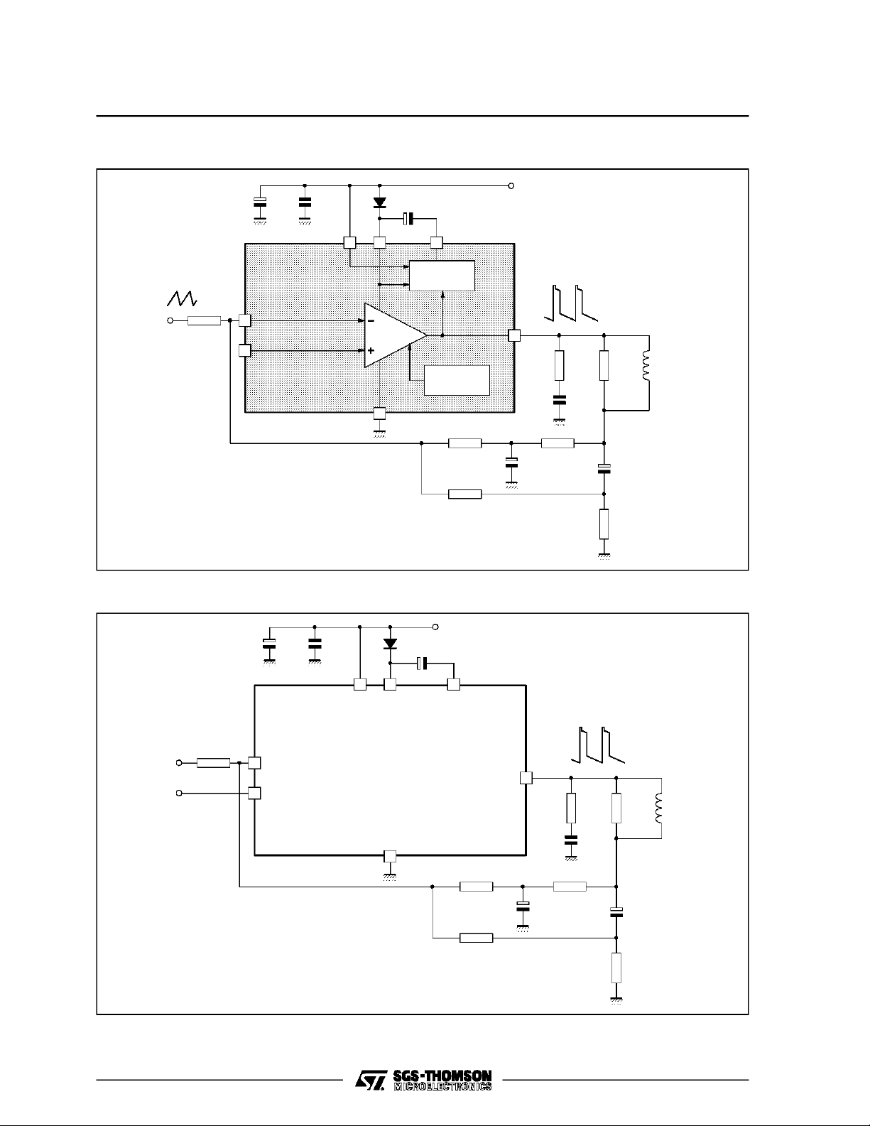
TDA8179S
BLOCK DIAGRAM
26 3
FLYBACK
GENERATOR
+V
S
APPLICATIONCIRCUIT
1
7
POWER
AMPLIFIER
THERMAL
PROTECTION
4
+V
S
26 3
5
YOKE
8179S-02.EPS
IN
V
REF
1
7
TDA8179S
4
OUT
5
Note : For values see ”Easy Design of Vertical Deflection Stages” (software available from our sales offices)
2/6
YOKE
8179S-03.EPS
Page 3
TDA8179S
ABSOLUTEMAXIMUM RATINGS
Symbol Parameter Value Unit
V
V
5,V6
V
1,V7
I
I
P
T
T
THERMALDATA
Supply Voltage (pin 2) 50 V
S
Flyback PeakVoltage 100 V
Amplifier Input Voltage + V
Output Peak Current
O
Non-repetitive, t = 2ms
f = 50 or 60Hz, t ≤ 10µs
f = 50 or 60Hz, t> 10µs
Pin 3 DCat V5<V
3
Pin 3 Peak FlybackCurrent at f = 50 or 60Hz, t
TotalPower Dissipation atTC=70oC20W
tot
Storage Temperature - 40, + 150
stg
Junction Temperature 0, +150
j
2
≤ 1.5ms
fly
S
2
2
1.8
100
1.8
A
mA
A
o
o
C
C
8179S-01.TBL
Symbol Parameter Value Unit
R
th (j-c)
Junction-case Thermal Resistance Max. 3
ELECTRICAL CHARACTERISTICS
=2.2V, VS=42V, TA=25oC, unlessotherwise specified)
(V
7
(refer to the test circuits- see Figure1 next page)
Symbol Parameter Test Conditions Min. Typ. Max. Unit
Operating Supply Voltage Range 10 42 V
S
Pin 2 Quiescent Current I3=0 I5= 0 10 20 mA
2
Pin 6 Quiescent Current I3=0 I5= 0 20 40 mA
6
Amplifier Bias Current V1= 1V - 0.2 - 1 µ
1
Scanning Voltage I3= 20mA 1.3 1.8 V
3L
Quiescent OutputVoltage
5
Output Saturation Voltage to GND I5= 1A 1.2 1.5 V
5L
Output Saturation Voltage to Supply - I5= 1A 2.2 2.6 V
5H
= 42V Ra= 3.9kΩ
V
S
= 35V Ra= 5.6kΩ
V
S
23.41724.2
17.82518.5
Diode Forward Voltage between Pins 5-6 ID= 1A 1.5 3 V
Diode Forward Voltage between Pins 3-2 ID= 1A 1.5 3 V
Input Resistance 200
1
Junction Temperaturefor Thermal
j
Shutdown
140
V
V
V
I
I
I
V
V
V
V
D5 - 6
D3 - 2
R
T
o
C/W
kΩ
8179S-02.TBL
A
V
o
C
8179S-03.TBL
3/6
Page 4

TDA8179S
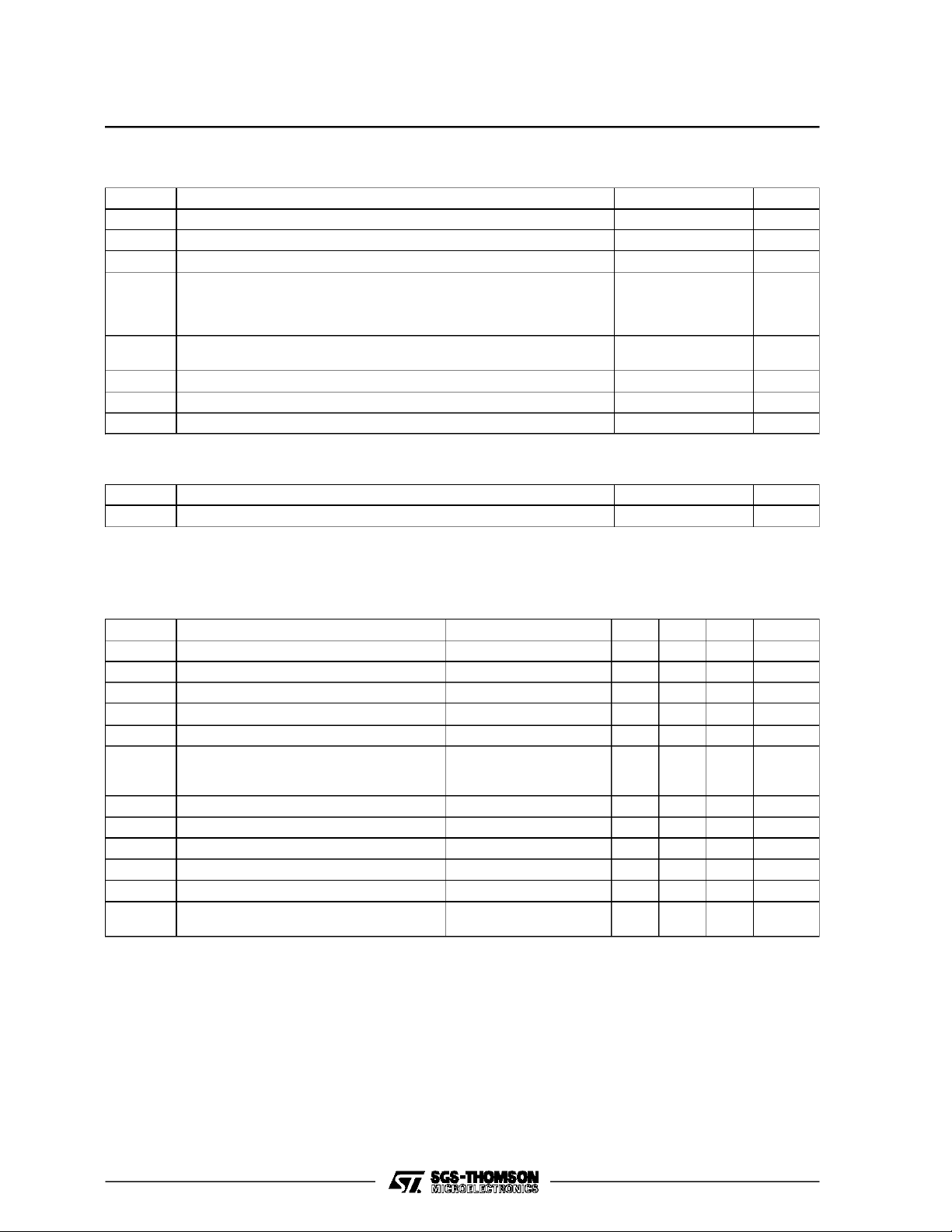
FIGURE1 : DC TestCircuits
Figure 1a: Measurementof I1,I2,I
I
2
26
TDA8179S
74
V
7
S1 : (a) I2and I6, (b) I
I
6
5
S1
1
1
Figure 1c: Measurementof V3L,V
6
5L
a
b
10k
Figure1b : Measurementof V
+V
S
26
Ω
I
1
1V
8179S-04.EPS
1V
TDA8179S
7
V
7
Figure1d : Measurementof V
5H
V
51
4
5
+V
S
5H
-I
5
8179S-05.EPS
26
1
7
3V
S1 : (a)V3L, (b) V
TDA8179S
V
7
5L
S1
a
3
5
4
V
3L
IorI
b
53
+V
V
S
5L
8179S-06.EPS
+V
S
26
TDA8179S
7
V
7
39kΩ
Re
51
4
V
5
8179S-07.EPS
4/6
Page 5
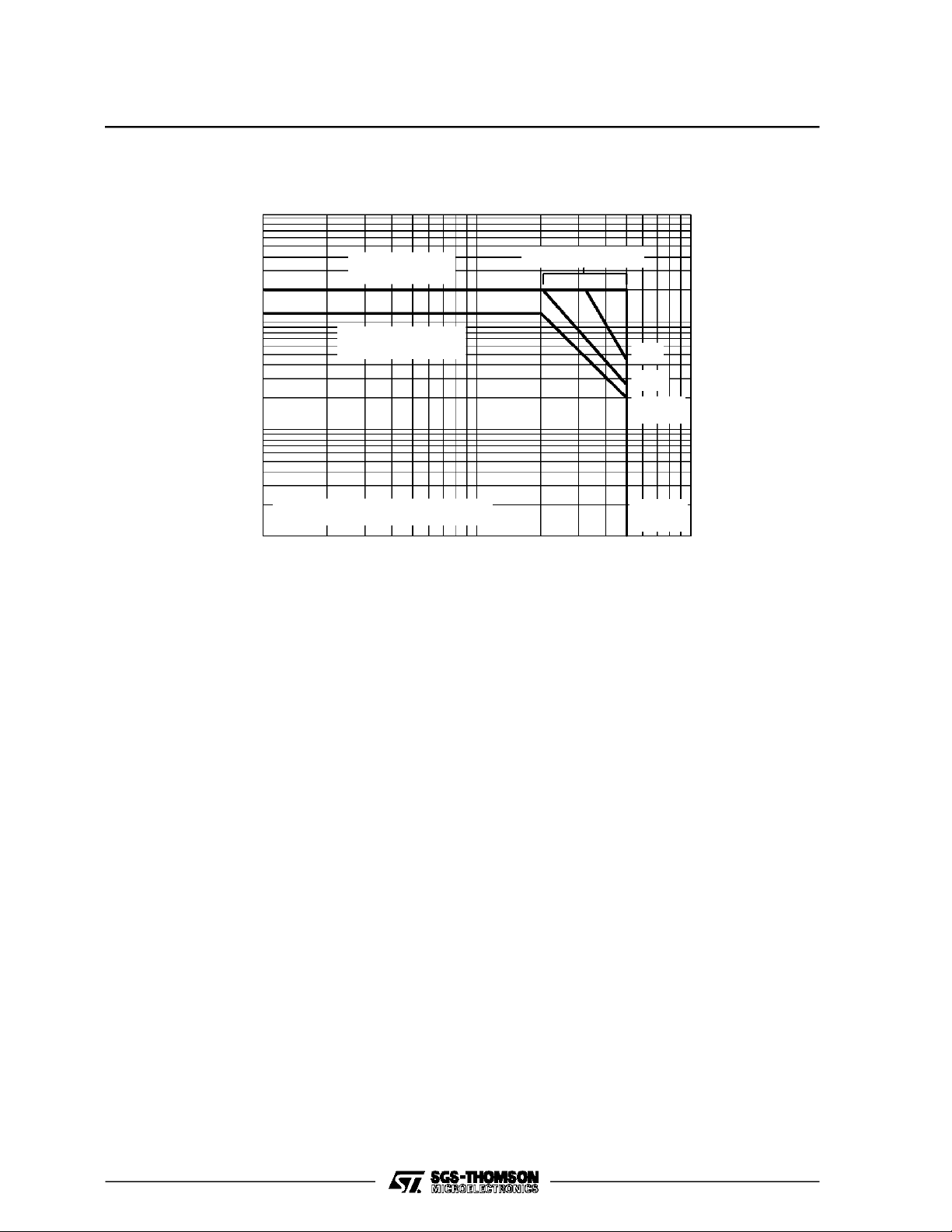
Figure 2 : SOAof Each Output PowerTransistorat TA=25oC
I (A)
10
C
TDA8179S
10
10
2
1.2
1
-1
-2
I max.pulsed
C
I max.continued
C
* For single non repetitive pulse
10110
Pulse Operation*
1ms
10ms
DC
Operation
V (V)
CE
2
8179S-08.EPS
5/6
Page 6
TDA8179S
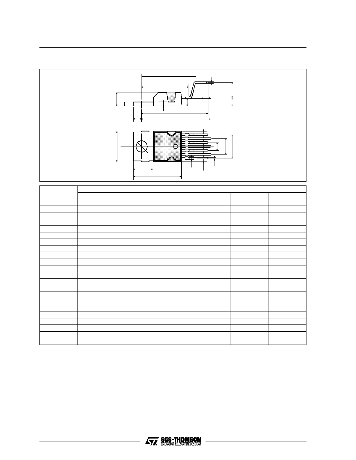
PACKAGE MECHANICAL DATA : HEPTAWATT
L
L1
A
C
H3
Dia.
L7
D1
L6
D
L2
L3L5
F1
E
MM1
G
G1
G2
F
H2
Dimensions Millimeters Inches
Min. Typ. Max. Min. Typ. Max.
A 4.8 0.189
C 1.37 0.054
D 2.4 2.8 0.094 0.110
D1 1.2 1.35 0.047 0.053
E 0.35 0.55 0.014 0.022
F 0.6 08 0.024 0.031
F1 0.9 0.035
G 2.41 2.54 2.67 0.095 0.100 0.105
G1 4.91 5.08 5.21 0.193 0.200 0.205
G2 7.49 7.62 7.8 0.295 0.300 0.307
H2 10.4 0.409
H3 10.05 10.4 0.396 0.409
L 16.97 0.668
L1 14.92 0.587
L2 21.54 0.848
L3 22.62 0.891
L5 2.6 3 0.102 0.118
L6 15.1 15.8 0.594 0.622
L7 6 6.6 0.236 0.260
M 2.8 0.110
M1 5.08 0.200
Dia. 3.65 3.85 0.144 0.152
Information furnishedis believed to beaccurate and reliable. However, SGS-THOMSON Microelectronicsassumes no responsibility
for the consequences of useof such information norfor anyinfringement of patents or other rights of third partieswhich may result
from itsuse. Nolicence isgranted by implication orotherwise under anypatent orpatent rights of SGS-THOMSON Microelectronics.
Specifications mentioned in this publication are subject to change without notice. This publication supersedes and replaces all
information previously supplied. SGS-THOMSON Microelectronics products are not authorized for use as critical components in life
support devices or systems without express written approval of SGS-THOMSON Microelectronics.
PM-HEPTV.EPS
HEPTV.TBL
6/6
1994 SGS-THOMSON Microelectronics - All RightsReserved
Purchase of I2C Components of SGS-THOMSON Microelectronics, conveys a license under the Philips
2
I
C Patent.Rights to use these components in a I2C system, is granted provided that the system conforms to
2
the I
C Standard Specificationsas defined by Philips.
SGS-THOMSON Microelectronics GROUP OF COMPANIES
Australia - Brazil - China - France - Germany - Hong Kong - Italy - Japan - Korea - Malaysia - Malta - Morocco
The Netherlands - Singapore - Spain - Sweden - Switzerland -Taiwan - Thailand - United Kingdom - U.S.A.
 Loading...