

Page 1

TV EAST/WEST CORRECTION CIRCUIT
.
LOW DISSIPATION
.
SQUARE GENERATOR FOR PARABOLIC
CURRENT SPECIALLY DESIGNED FOR
SQUARE C.R.T. CORRECTION
.
EXTERNAL KEYSTONE ADJUSTMENT
(symmetry of the parabola)
.
INPUT FOR DYNAMIC FI ELD CORRECTION
(beam current change)
.
STATIC PICTURE WIDTH ADJUSTMENT
.
PULSE-WIDTH MODULATOR
.
FINAL STAGE D-CLASS WITH ENERGY
REDELIVERY
.
P ARASITIC PARABOLA SUPPRESSION,
DURING FLYBACK TIME OF THE
VERTICAL SAWTOOTH
TDA8145
FOR SQUARE TUBES
POWERDIP8
(Plastic Package)
(Th = 0.4mm)
DESCRIPTION
The TDA8145 is a monolithic integrated circuit in a
8 pin minidip plastic package designed for use in
the square C.R.T. east-west pin-cushion correction
by driving a diode modulator in TV and monitor
applications.
PIN CONNECTIONS (top view)
KEYSTONE CORRECTION INPUT
FRAME SAWTOOTH CURRENT INPUT
CURRENT REFERENCE
GND
1
2
3
4
ORDER CODE :
8
NON-INVERTING INPUT 100
7
PARABOLA OUTPUT INVERTING INPUT
+V
6
5
S
OUTPUT
TDA8145
A CURRENT SINK
µ
October 1998
8145-01.EPS
1/5
Page 2
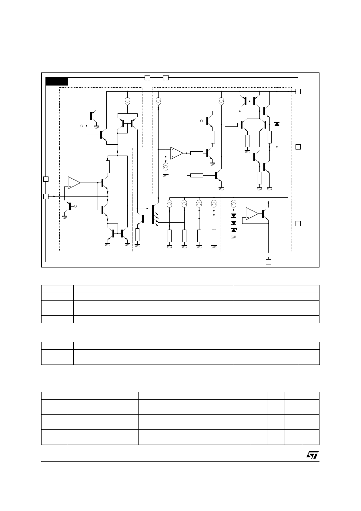
TDA8145
SCHEMATIC DIAGRAM
TDA8145
1
2
I
IN
VS - 3 V
Q7
CURRENT LIMITER
BE
OP1
VS - 6 V
BE
Q1
Q2
R5
Q5
Q6
Q8 Q9
Q4Q13
Q10
7
R9
8
COMPARATOR AND OUTPUT STAGE
V
OP2
Q11
R10 R11 R12 R13
+V
6
S
Q14
Q13
REF
R5
R6
Q12
R7
R2
Q21
D2
D3
Z1
Q15
Q16
Q20
Q22
D1
OUTPUT
5
I
REF
4
GND
Q18Q17
R3
R4
Q19
R8
OP3
FULL-WAVE RECTIFIER
PARABOLA NETWORK
CURRENT REFERENCE
3
ABSOL UT E MAXIMU M RATINGS
Symbol Parameter Value Unit
V
s
I
s
P
tot
, TjStorage and Junction Temperature – 25 to 150
T
stg
Supply Voltage 35 V
Supply Current 500 mA
Power Dissipation at T
= 50 °C 500 mW
amb
THERMAL DATA
Symbol Parameter Value Unit
R
th (j–c)
R
th (j–a)
ELECTRICAL CHARACTERISTICS (T
Thermal Resistance Junction-ambient Max. 100
Thermal Resistance Junction-pin 4 Max. 70
= 25oC, VS = 26V, Vfr = 0, S1 and S2 in "a" position, refer
amb
°
°
to the test circuit unless otherwise specified)
Symbol Parameter Test Conditions Min. Typ. Max. Unit
V
V
– I
V
7(A)
V
7(B)
Supply Voltage 17 24 30 V
S
I
Supply Current 4.5 7 mA
S
Internal Reference Voltage 7.6 8.0 8.8 V
ref
Internal Reference Current V
ref
(*)
Pin 7 Output Voltage Ifr = 0 µA 15.3 16.0 16.7 V
(*)
Pin 7 Output Voltage Ifr = 30 µA15V
/R3 0.73 mA
ref
C
°
C/W
C/W
8145-02.EPS
8145-01.TBL
8145-02.TBL
8145-03.TBL
2/5
Page 3

TDA8145
ELECTRICAL CHARACTERISTICS (T
= 25oC, VS = 26V, Vfr = 0, S1 and S2 in "a" position, refer
amb
to the test circuit unless otherwise specified) (continued)
Symbol Parameter Test Conditions Min. Typ. Max. Unit
V
− V
7A
V7A − V
− V
V
7A
V7A − V
pp
7B
7C
7C
7D
7F
0.26
0.70
– 40 40 mV
b 0.8 1.5 V
→
b 1.2 1.7 V
→
66
K
K2
V
∆
V
SATL
V
SATH
V
Parabola Coefficient
1
(see Figure 2)
Parabola Coefficient
(see Figure 2)
(*)
7
I
Current Source S1 → b 100
8
Saturation Voltage Io = 400 mA Sink S2 → b12V
Saturation Voltage Io = 100 mA Source S2 → cS1
Forward Voltage Io = 400 mA S2 → dS1
F
I
Frame Sawtooth Current Vfr = 6.6 V
fr
K1 =
K
=
2
V7 = V7E – V
∆
Figure 1 : T es t Circuit
V
S
R7 R6
10kΩ 10kΩ
I
FR
V
FR
R1
10k
Ω
R3
11k
Ω
R2
V
REF
2
1
3
7
TDA8145
V
R8
20k
F
5
Ω
6
84
V
SATH
a
S2
d
I
F
b
c
-I
O
I
O
V
SATL
A
µ
A
µ
8145-04.TBL
Figure 2 : Parabola Characteristics
V
7E
-60 0 15 30
a
V7 (V)
V
7A
S1
b
8145-03.EPS
V
7B
V
7C
V
7D
V
7F
36
60
I
FR
(µA)
8145-04.EPS
3/5
Page 4

TDA8145
APPLICATION CIRCUIT WITH KEYSTONE CORRECTION
Line Transformer
(L.T.)
LM
L1
10mH
R3 RT2
Pin-cushion
adjustment
V
FRAME
R1 =
66µA
PP
V
Pin 1
Voltage
FRAME
Keystone
Adj.
CIRCUIT OPERATION (see the schematic diagram)
A differential amplifier OP1 is driven by a vertical
frequency sawtooth current of ± 33µA which is
produced via an external res istor from the sawtooth
voltage. The non–inverting input of this amplifier is
connected with a reference voltage corresponding
to the DC level of the sawtooth voltage. This DC
voltage should be adjustable for the keystone correction. The rectified output current of this amplifier
drives the parabola network which provides a parabolic output current.
This output current produces the corresponding
voltage due to the voltage drop across the external
resistor at pin 7.
If the input is overmodulated (> 40µA) the internal
4.7k
5
2
TDA8145
1
3 4 8
RT1
100k
Ω
R2
12k
Ω
Ω
47k
Hfly
from L.T.
Ω
7
R5 RT3
C3
4.7nF
R4
18k
Ω
6
C2
100nF
D1
1N4148
1k
Ω
H. Width
current is limited to 40µA. This limitation can be
used for suppressing the parasitic parabolic current
generated during the flyback time of the frame
sawtooth.
A comparator OP2 is driven by the parabolic current. The second input of the comparator is connected with a horizontal frequency sawtooth
voltage the DC level of whic h can be changed by
the external circuitry for t he adjus tment of the picture width.
The horizontal frequency pulse–width modulated
output signal drives the final stage. It consists of a
class D push–pull output amplifier that drives, via
an external inductor, the diode modulator.
C1
47nF
V
S
8145-05.EPS
4/5
Page 5

TDA8145
PACKAGE MECHANICAL DATA
8 PINS - PLASTIC POWERDIP
Dimensions
Min. Typ. Max. Min. Typ. Max.
A 3.3 0.130
a1 0.7 0.020
B 1.39 1.65 0.055 0.065
B1 0.91 1.04 0.036 0.041
b 0.5 0.020
b1 0.38 0.5 0.015 0.020
D 9.8 0.386
E 8.8 0.346
e 2.54 0.100
e3 7.62 0.300
e4 7.62 0.300
F 7.1 0.280
I 4.8 0.189
L 3.3 0.130
Z 0.44 1.6 0.017 0.063
Information furnished is believed to be accurate and reliable. However, STMicroelectronics assumes no responsibility for the
consequences of use of such information nor for any infringement of patents or other rights of third parties which may result from
its use. No licence is granted by implication or otherwise under any patent or patent rights of STMicroelectronics. Specifications
mentioned in this publication are subject to change without notice. This publication supersedes and replaces all information
previously supplied. STMicroelectronics products are not authorized for use as critical components in life support devices or sys tem s
without express written approv al of STMi cr oelec troni cs.
Purchase of I
Rights to use these components in a I
Australia - Brazil - Canada - China - France - Germany - Italy - Japan - Korea - Malaysia - Malta - Mexico - Morocco - The Neth erlands
2
C Components of STMicroelectronics, conveys a license under the Philips I2C Pate n t .
Singapore - Spain - Sweden - Switzerland - Taiwan - Thailand - United Kingdom - U.S.A.
Millimeters Inches
The ST logo is a registered trademark of STMicroelectronics
© 1998 STMicroelectronics - All Rights Reserved
2
2
the I
C Standard Specifications as defined by Phili ps.
STMicroelectronics GROUP OF COMPANIES
C system, is granted provided that the system conforms to
http://www.st.com
5/5
PM-DIP8.EPS
DIP8PW.TBL
 Loading...