

Page 1
5.1V AN D ADJUSTABLE VOLTAGE REGULATOR
.
OUTPUT CURRENTS UP TO 750mA
.
FIXED PRECISION OUTPUT 1 VOLTAGE
5.1V ± 2%
.
OUTPUT 2 VOLTAGE PROGRAMMABLE
FROM 2.8 TO 16V
.
OUTPUT 1 WITH RESET FACILITY
.
OUTPUT 2 WITH DISABLE BY TTL INPUT
.
SHORT CIRCUIT PROTECTION AT BOTH
OUTPUTS
.
THERMAL PROTECTIO N
.
LOW DROP OUTPUT VOLTAGE
TDA8139
WITH DISABLE AND RESET
DESCRIPTION
The TDA8139 is a monolithic dual positiv e volt age
regulator designed to provide precision out put voltages of 5.1V and adjustable at currents up to
750mA.
An internal reset circuit generates a reset pulse
when the output 1 decrease below the regulated
voltage value.
Output 2 can be disabled by TTL input.
Short circuit and thermal protect ions are inclu ded.
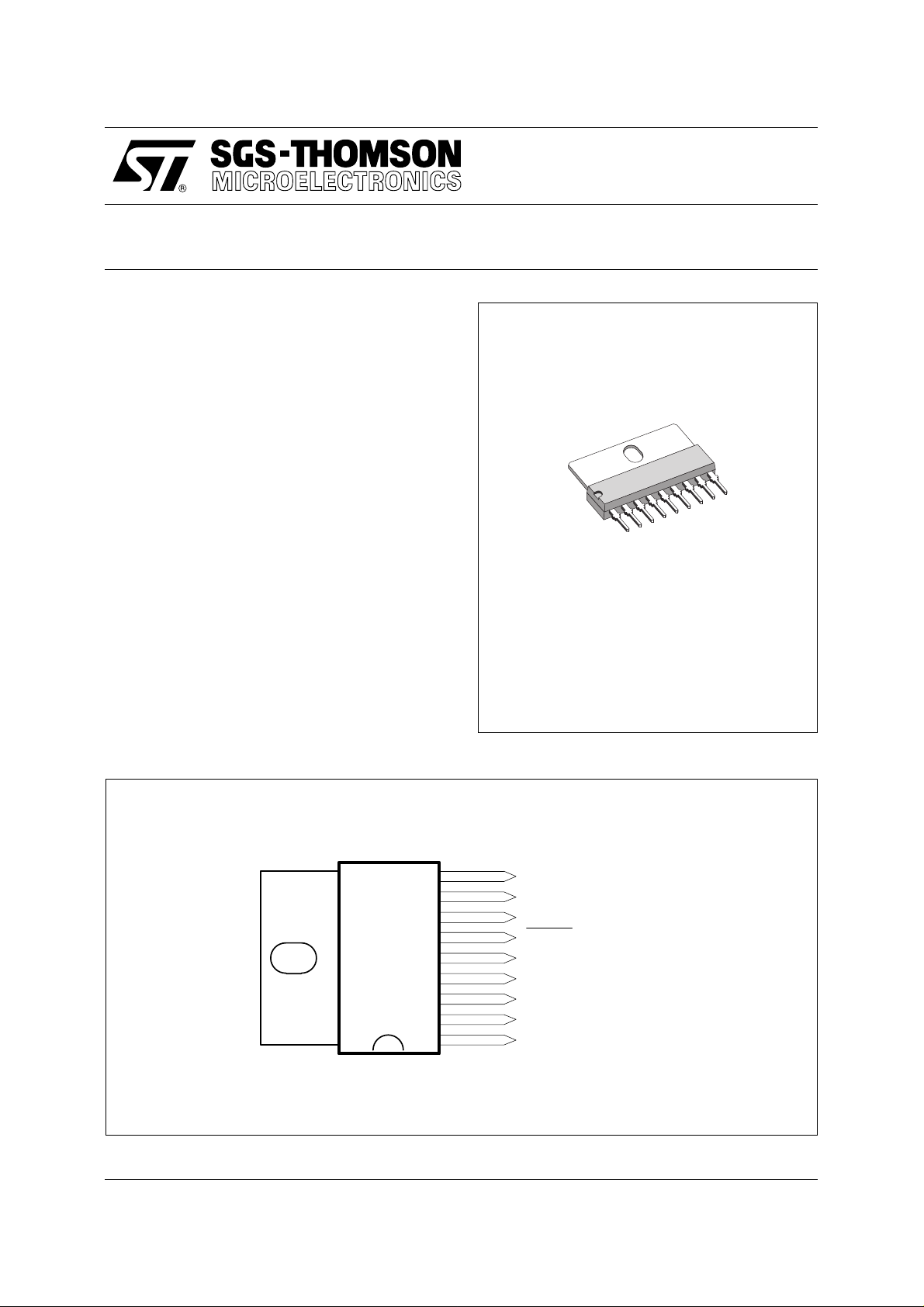
PIN CONNECTIONS
9
8
7
6
5
4
3
2
1
SIP9
(Plastic Package)
ORDER CODE : TDA8139
OUTPUT 1
OUTPUT 2
PROGRAM
RESET
GROUND
DISABLE
DELAY CAPACITOR
INPUT 2
INPUT 1
September 1993
8139-01.EPS
1/5
Page 2
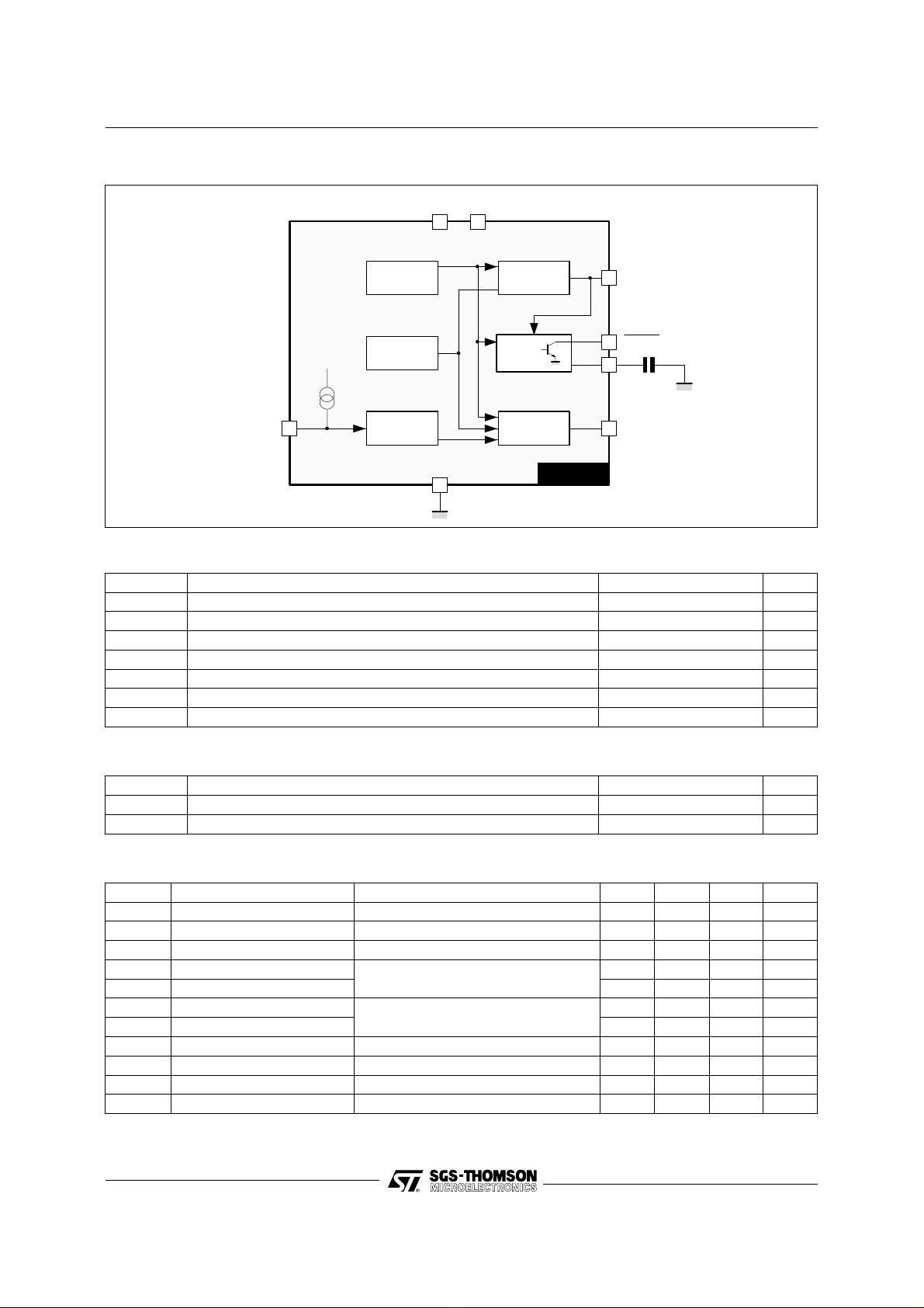
TDA8139
BLOCK DIAGRAM
IN 2IN 1
12
REFERENCE
PROTECTION
4
DISABLE
5
OUT 1
RESET
OUT 2
TDA8139
OUT 1
9
6
RESET
3
DELAY
CAPACITOR
8
OUT 2DISABLE
ABSOLUTE MAXIMUM RATINGS
Symbol Parameter Value Unit
V
V
V
I
O1, 2
T
T
IN
DIS
RST
P
STG
DC Input Voltage Pin 1, 2 20 V
Disable Input Voltage Pin 4 20 V
Output Voltage at Pin 6 20 V
Output Currents Internally Limited
Power Dissipation Internally Limited
t
Storage Temperature – 65 to + 150 °C
unction Temperature 0 to + 150 °C
J
8139-02.EPS
8139-01.TBL
THERMAL DATA
Symbol Parameter Value Unit
R
TH(j-c)
T
Thermal Resistance Junction-case Max. 8 °C/W
Recommended Junction Temperature Max. 130 °C
J
ELECTRICAL CHARACT E RIS TICS ( VIN = 7V ; Tj = 25oC unless otherwise specified)
Symbol Parameter Test Conditions Min. Typ. Max. Unit
Output Voltage IO1 = 10mA 5 5.1 5.2 V
O1
Output Voltage IO2 = 10mA 2.8 16 V
O2
Dropout Voltage I
Line Regulation 1 7V < V
O1
Line Regulation 2 100 mV
O2
Load Regulation 1 5mA < I
O1
Load Regulation 2 200 mV
O2
Quiescent Current IO1 = 10mA, Output 2 Disabled 2 mA
I
Q
= 750mA 1.4 V
O1, 2
IN1
VO2 : 10V, I
O1, 2
< 14V, 12V < V
= 200mA
O1, 2
< 0.6A, @ VO2 = 10 V 100 mV
< 18V, @
IN2
Reset Threshold Voltage (K = VO1) K – 0.4 K – .25 K – 0.1 V
Reset Threshold Hysteresis (see circuit description) 20 50 75 mV
RTH
Reset Pulse Delay at Pin 6 Ce = 100nF (see circuit description) 25 ms
RD
50 mV
2/5
V
V
V
V
V
V
V
V
O1RST
V
IO1, 2
t
8139-02.TBL
8139-03.TBL
Page 3

TDA8139
ELECTRICAL CHARACT E RIS TICS ( VIN = 7V ; Tj = 25oC unless otherwise specified)
Symbol Parameter Test Conditions Min. Typ. Max. Unit
V
I
K
O1,2
I
O1,2 sc
V
DISH
V
DISL
I
DIS
V
T
Note 1 : The output short circuit currents are tested one channel at time.
During a short circuit a large consumption of power occurs, but the thermal protection circuit prevents any excessive temperature.
Safe permanent short-circuit is only guaranteed for input voltages up to 16V .
Figure 1
Saturation Volt. at Pin 6 in Reset Condition I5 = 5mA 0.4 V
RL
Leakage Current at Pin 6 in Normal Condition V5 = 10V 10 µA
RH
Output Volt. Thermal Drift
∆V
K
=
0
⋅ 10
o
∆T ⋅ V
6
O
100 ppm/°C
Tj = 0 to + 125°C
Short Circ. Ouput Current VIN = 7V 1.6 A
V
= 16V, (see note 1) 1 A
IN
Disable Volt. at Pin 4 High (out 2 active) 2 V
Disable Volt. at Pin 4 Low (out 2 disabled) 0.8 V
Disable Bias Current at Pin 4 0V < V
Pin 7 2.5 V
ref
Junction Temp. for Thermal Shut Down 145 °C
jsd
< 7V -100 2 µA
DIS
10µA
b
-
+
OUT 1
REF
2.5V
9
a
+
50
3
RESET
6
8139-04.TBL
Figure 2
5.1V
4.9V
4.85V
RESET
REG
C
e
T
D
2.5V 0.6V
∆
T
D
8139-03.EPS
VOUT LOW
8139-04.EPS
3/5
Page 4

TDA8139
CIRCUIT DESCRIPTION
The TDA8139 is a dual voltage regulator with Reset
and Disable.
The two regulation parts are supplied from one
voltage reference circuit trimmed by zener zap
during EWS test. Since the supply voltage of this
last is connected at Pin 1 (V
not work if the Pin 1 is not supplied.
The outputs stages have been realized in darlington configuration with a drop typical of 1.2V.
The disable circuit, switch-off the output 2 if a
voltage lower than 0.8V is applied at pin 4.
TYPICAL APPL ICA T ION
), the regulator 2 will
IN1
RESET
63
The Reset circuit checks the voltage at the output
1. If this one goes below V
- 0.25V (4.85V T yp.),
OUT
the comparator "a" (see Figure 1) discharges rapidly the capacitor Ce and the reset output goes at
once low. When the voltage at the OUT 1 rises
above V
-0.2V (4.9V Typ.), the voltage V
OUT
increases linearly to 2.5V corresponding to a delay
2.5
t
following the low : td =
d
Ce ⋅
10µA
V
(see figure 2),
then the reset output goes high again. To avoid
glitches in the reset output, the second comparat or
"b" has a large hysteresis (1.9V).
R1 + R
2
R
1
Ce 0.1µF
VO2 = V
REF
typ. val R1 = 2.2Ω
Ce
V
IN1
1
9
V
O1
TDA8139
V
IN2
C1 C2 C3
2
45
DISABLE
C1 to C4 = 10µF
7
8
C4
R1
V
O2
R2
8139-05.EPS
4/5
Page 5

PACKAGE MECHANICAL DATA
9 PINS - PLASTIC SIP
TDA8139
C
c2
A
c1
Dimensions
L2
D
L1
19
a1
L
e3
N
M
b1
b3
e
B
L3
d1
Millimeters Inches
Min. Typ. Max. Min. Typ. Max.
A 7.1 0.280
a1 2.7 3 0.106 0.118
B 24.8 0.976
b1 0.5 0.020
b3 0.85 1.6 0.033 0.063
C 3.3 0.130
c1 0.43 0.017
c2 1.32 0.052
D 21.2 0.835
d1 14.5 0.571
e 2.54 0.100
e3 20.32 0.800
L 3.1 0.122
L1 3 0.118
L2 17.6 0.693
L3 0.25 0.010
M 3.2 0.126
N 1 0.039
Information furnished is believed to be accurate and reliable. However, SGS-THOMSON Microelectronics assumes no responsibility
for the consequences of use of such information nor for any infringement of patents or other rights of third parties which may result
from its use. No licence is granted by implication or otherwi se under any patent or patent rights of SGS-THOMSON Microelectronics.
Specifications mentioned in this publication are subject to change without notice. This publication supersedes and replaces all
information previously suppli ed. SGS-THOMSON Microele ctronics products are not authorized for use as critical components in life
support devices or systems without express written approval of SGS-THOMSON Microelectronics.
PM-SIP9.EPS
SIP9.TBL
© 1994 SGS-THOMSON Microelectronics - All Rights Reserved
2
Purchase of I
2
C Patent. Rights to use these components in a I2C system, is granted provided that the system conforms to
I
Australia - Brazil - China - France - Germany - Hong Kong - Italy - Japan - Korea - Malaysia - Malta - Morocco
The Netherlands - Singapore - Spain - Sweden - Switzerland - Taiwan - Thailand - United Kingdom - U.S.A.
C Components of SGS-THOMSON Microelectronics, conveys a license under the Philips
2
C Standard Specifications as defined by Philips.
the I
SGS-THOMSON Microelectronics G ROUP OF COMPANIES
5/5
 Loading...