

Page 1

DATA SH EET
Product specification
Supersedes data of 1998 Jan 08
File under Integrated Circuits, IC02
1999 Aug 20
INTEGRATED CIRCUITS
TDA8051
QPSK receiver
Page 2

1999 Aug 20 2
Philips Semiconductors Product specification
QPSK receiver TDA8051
FEATURES
• High operating input sensitivity
• Gain controlled amplifier
• PLL controlled carrier frequency
• Low crosstalk between I and Q channel outputs
• 3-wire transmission bus
• 5 V supply voltage.
APPLICATIONS
• BPSK/QPSK demodulation.
GENERAL DESCRIPTION
This TDA8051 is a monolithic bipolar IC intended for
Quadrature Phase Shift Key (QPSK) demodulation. It
includes:
• Low noise RF and gain controlled amplifier
• Two matched mixers
• Symmetrical Voltage Controlled Oscillator (VCO) with
0to90°signal generator whosefrequency is controlled
by an integrated Phase Lock Loop (PLL) circuit.
• Two matched amplifiers for output base-band active
filtering and output buffers
The gain control is produced by output level detection
compared with an external pre-fixed reference. The PLL
consists of:
• Divide by four preamplifier
• 12-bit programmable main divider
• Crystal oscillator with 8-bit programmable reference
divider
• Phase/frequency detector combined with charge pump
to drive tuning amplifier
• 30 V output
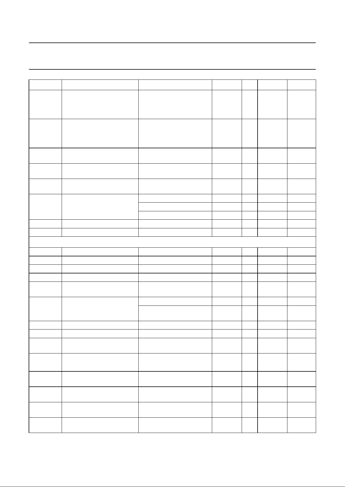
QUICK REFERENCE DATA
All AC units are RMS values unless otherwise specified.
ORDERING INFORMATION
SYMBOL PARAMETER MIN. TYP. MAX. UNIT
V
CC
supply voltage range 4.75 5.00 5.25 V
f
I(LNA)
input carrier frequency at LNA input 44 − 130 MHz
V
I(LNA)
input level at LNA input −30 − 0 dBmV
∆Φ
I-Q
phase error between I and Q channels −±3−deg
∆G
I-Q
gain error between I and Q channels −±1−dB
α
CT(I-Q)
crosstalk between I and Q channels −−30 − dBc
IM3 3rd-order intermodulation distortion in
I and Q channels (0 dBmV at LNA_IN)
−−−45 dBc
V
o
voltage output on pin I_OUT and Q_OUT − 48 − dBmV
f
step
step at output 50 − 250 kHz
f
xtal
crystal frequency 1 − 4 MHz
T
amb
operating ambient temperature 0 − 70 °C
TYPE NUMBER
PACKAGE
NAME DESCRIPTION VERSION
TDA8751T SO32 plastic small outline package; 32 leads; body width 7.5 mm SOT287-1
Page 3
1999 Aug 20 3
Philips Semiconductors Product specification
QPSK receiver TDA8051
This text is here in white to force landscape pages to be rotated correctly when browsing through the pdf in the Acrobat reader.This text is here in
_white to force landscape pagestoberotated correctly when browsing through the pdf in the Acrobat reader.This text is here inThis text is here in
white to force landscape pages to be rotated correctly when browsing through the pdf in the Acrobat reader. white to force landscape pages to be ...
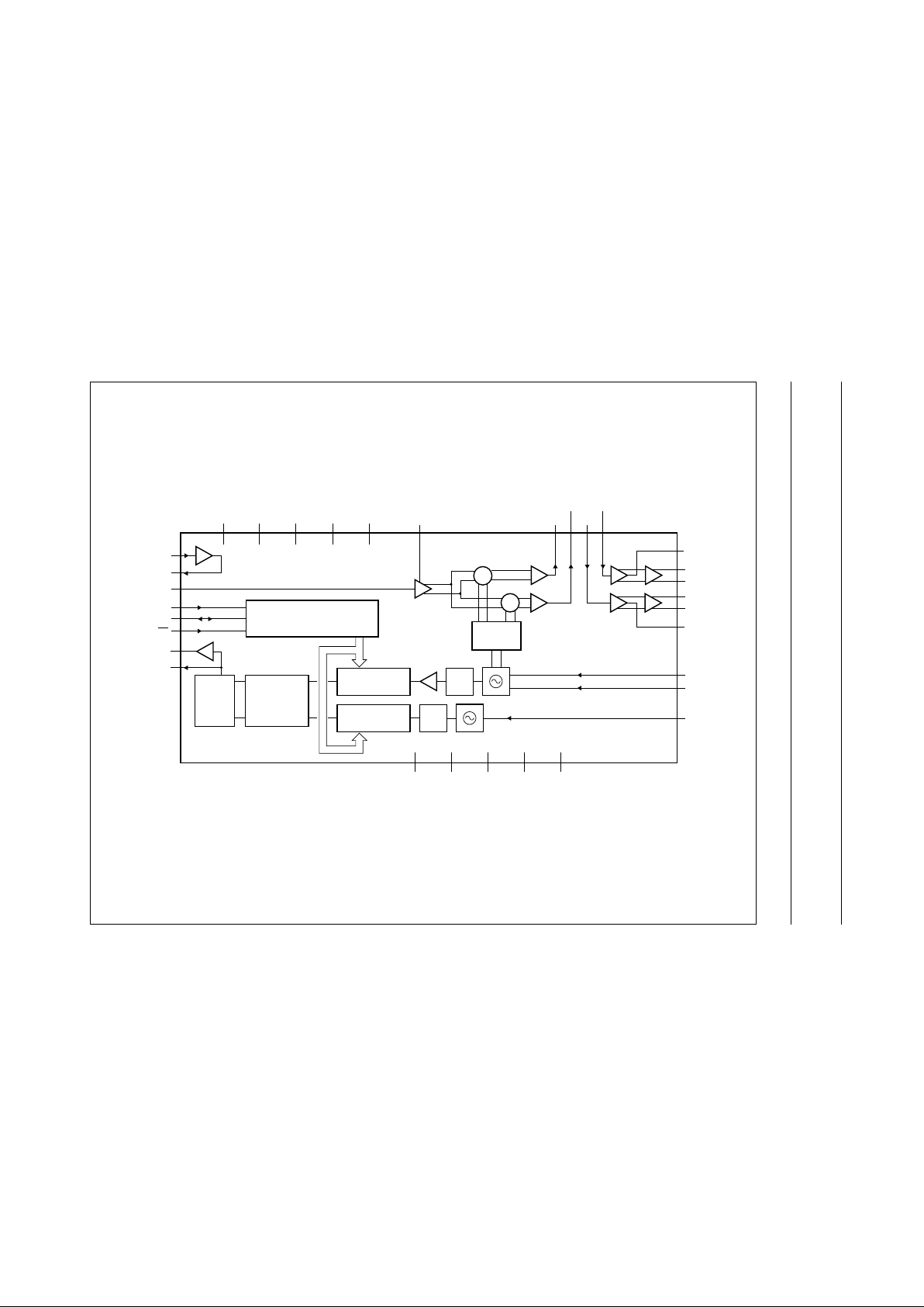
BLOCK DIAGRAM
handbook, full pagewidth
FCE112
1/2
90¡ 0¡
×
×
5
TDA8051
28
1
3
2
32
31
30
21
22
12
29 4
I_OUT1
11
I_OUT2
Q_OUT2
TKB
TKA
OSC_IN
I_OUTC
I_OUT
Q_OUTC
Q_OUT
AGC_IN
27
OUTVCC
13
DVCC
25
A3VCC
23
A2VCC
6
8
7
A1VCC
LNA_OUT
9
LNA_IN
14
CLK
15
DATA
16
EN
19
TUNE
18
CP
DEMOD_IN
Q_OUT1
Q_IN1
I_IN1
1/4
PROGRAMMABLE
MAIN DIVIDER
3-WIRE BUS TRANSCEIVER
DIGITAL
PHASE
COMPARATOR
CHARGE
1/2
PROGRAMMABLE
REF DIVIDER
17
TEST
n.c.
10
A1GND24A2GND26OUTGND20DGND
Fig.1 Block diagram.
Page 4
1999 Aug 20 4
Philips Semiconductors Product specification
QPSK receiver TDA8051
PINNING
SYMBOL PIN DESCRIPTION
I_OUT 1 I data buffered balanced output
I_OUTC 2 I data buffered balanced output
I_OUT2 3 I data filtered output
I_IN1 4 input to active filter amplifier for
I data
I_OUT1 5 I data raw output
A1VCC 6 analog supply voltage 1
DEMOD_IN 7 demodulator RF input
LNA_OUT 8 low noise amplifier RF output
LNA_IN 9 low noise amplifier RF input
A1GND 10 analog ground 1
AGC_IN 11 AGC control voltage input
OSC_IN 12 oscillator input
DVCC 13 digital supply voltage
CLK 14 3-wire bus serial control clock
DATA 15 3-wire bus serial control data
EN 16 3-wire bus serial control enable
(active LOW)
TEST 17 not connected
CP 18 charge pump output for PLL loop
filter
TUNE 19 tuning voltage output
DGND 20 digital ground
TKB 21 VCO tank circuit input
TKA 22 VCO tank circuit input
A2VCC 23 analog supply voltage 2
A2GND 24 analog ground 2
A3VCC 25 analog supply voltage 3
OUTGND 26 output amplifiers ground
OUTVCC 27 output amplifiers supply voltage
Q_OUT1 28 Q data raw output
Q_IN1 29 input to active filter amplifier for
Q data
Q_OUT2 30 Q data filtered output
Q_OUTC 31 Q data buffered balanced output
Q_OUT 32 Q data buffered balanced output
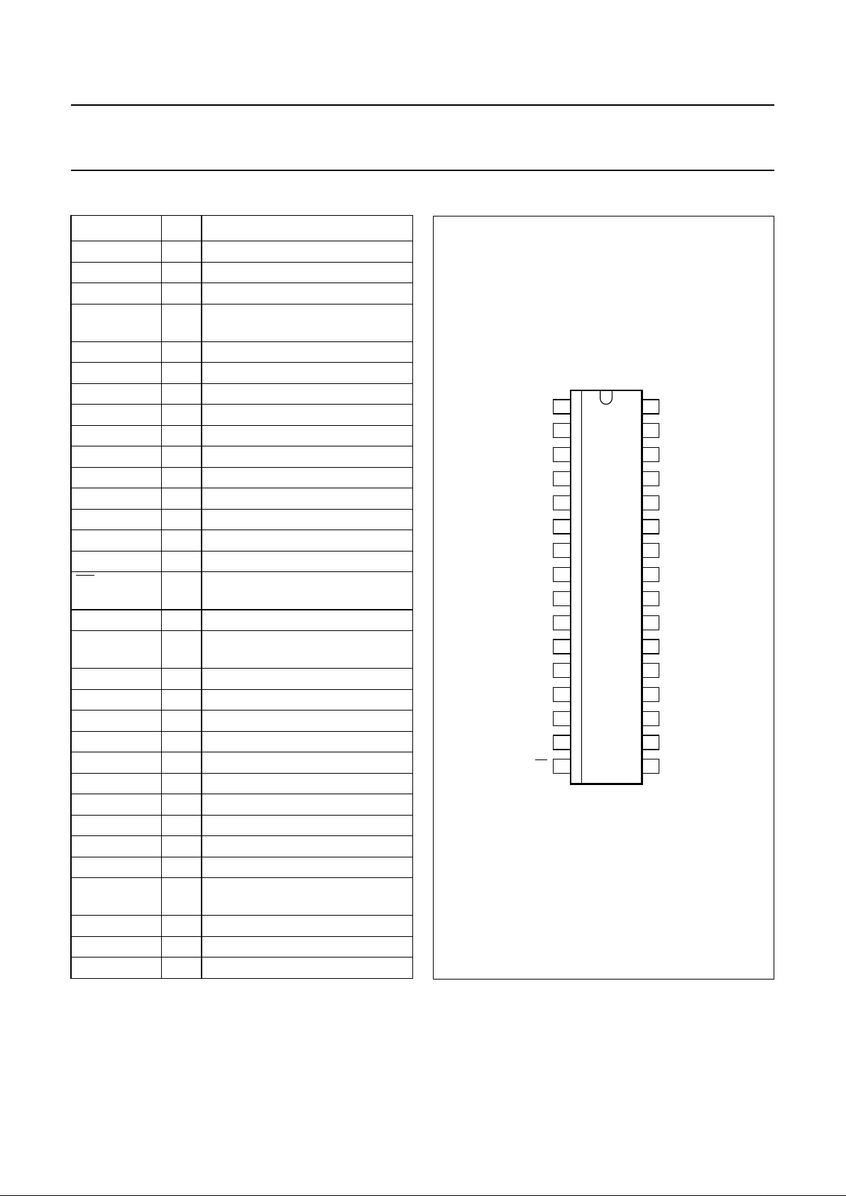
handbook, halfpage
TDA8051
FCE171
1
2
3
4
5
6
7
8
9
10
11
12
13
14
15
16
32
31
30
29
28
27
26
25
24
23
22
21
20
19
18
17
I_OUT
I_OUTC
I_OUT2
I_IN1
I_OUT1
A1VCC
DEMOD_IN
LNA_OUT
LNA_IN
A1GND
AGC_IN
OSC_IN
DVCC
CLK
Q_OUT
Q_OUTC
Q_OUT2
Q_IN1
OUTVCC
OUTGND
Q_OUT1
A3VCC
A2GND
A2VCC
TKA
TKB
DGND
TUNE
DATA
EN
CP
TEST
Fig.2 Pin configuration.
Page 5

1999 Aug 20 5
Philips Semiconductors Product specification
QPSK receiver TDA8051
FUNCTIONAL DESCRIPTION
The QPSK modulated signal is applied to the input as an
asymmetrical RF signal in the bandwidth 44 to 130 MHz.
The spectrum extension to this waveform must be limited
by a band-pass filter superseding the IC.
The RF input is either the LNA input, if the level is
−30 to 0 dBmVrms, or the DEMOD input if the level is
−20 to +10 dBmVrms. The amplified RF signal is then
mixed with two clocks in quadrature to provide the
base-band demodulated In-phase (I) and Quad-phase (Q)
signals.
The VCO operates at twice the RF carrier frequency in the
bandwidth 88 - 260 MHz (one octave), therefore the
0to90° clocks are generated by a divider by 2.
The VCO frequency can be programmed by an integrated
PLL that tunes the external LC tank circuit.
The raw I and Q generated signals contain spurious
spikes, therefore each signal is passed through a third
order active low-pass filter (RC cell + Sallen-Key
structure), whose cut-off frequency is set by external
components. The filtered I and Q data signals are then
amplified to provide balanced buffer outputs.
The data sent to the PLL is loaded in bursts, framed by
signal EN. Programming clock edges, together with their
relevant data bits, are ignored until EN becomes active
(LOW). The internal latches are updated with the latest
programming data when EN returns to inactive (HIGH).
The last 14 bits only are retained within the programming
register. No check is made on the number of clock pulses
received while programming is enabled. An active clock
edge causing a shift of the data bits is generated when
EN goesHIGH while CLOCK isstillLOW. The main divider
ratio and the reference divider ratio are provided via the
serial bus (see Table 1).
LIMITING VALUES
In accordance with the Absolute Maximum Rating System (IEC 134).
HANDLING
HBM ESD: The IC pins withstand 2 kV except pin 26 (1750 V).
MM ESD: The IC pins withstand 100 V except pins 2 and 31 (75 V).
THERMAL CHARACTERISTICS
SYMBOL PARAMETER MIN. MAX. UNIT
V
CC
supply voltage −0.3 6.0 V
V
(max)
maximum voltage on all pins except pin 9 (5 V) −0.3 V
CC
V
t
sc
maximum short circuit duration on outputs − 10 s
T
stg
storage temperature −40 +150 °C
T
j(max)
maximum junction temperature − 150 °C
T
amb
operating ambient temperature 0 70 °C
V
CC(tune)
tuning voltage supply −0.3 30 V
SYMBOL PARAMETER CONDITIONS VALUE UNIT
R
th(j-a)
thermal resistance from junction to ambient in free air 65 K/W
Page 6

1999 Aug 20 6
Philips Semiconductors Product specification
QPSK receiver TDA8051
CHARACTERISTICS
Measured in application circuit with the following conditions: VCC=5V; T
amb
=25°C. All AC units are RMS values,
unless otherwise specified.
SYMBOL PARAMETER CONDITIONS MIN. TYP. MAX. UNIT
Supplies
V
CCA1
analog supply voltage 4.75 5 5.25 V
I
CCA1
analog supply current − 23 − mA
V
CCA2
analog supply voltage 4.75 5 5.25 V
I
CCA2
analog supply current − 18 − mA
V
CCA3
analog supply voltage 4.75 5 5.25 V
I
CCA3
analog supply current − 29 − mA
V
cc(o)
output supply voltage 4.75 5 5.25 V
I
cc(o)
output supply current − 17 − mA
V
CCD
digital supply voltage 4.75 5 5.25 V
I
CCD
digital supply current − 13 − mA
V
CC(tune)
tuning supply voltage −−30 V
Low noise amplifier: Rs=75Ω/Ri=75Ω unless otherwise specified
V
I(DC)
DC input level internally set − 0.85 − V
V
i
input level −30 − 0 dBmV
f
i
input carrier frequency 44 − 130 MHz
R
i
input resistance − 75 −Ω
C
i
input capacitance − 2.5 − pF
R
LLNA
input return loss −−15 − dB
NF
LNA
noise figure − 711 dB
V
leak(LO)
LO leakage on pin at LNA_IN f
N × LO
= 140 − 860 MHz;
pin LNA_OUT connected to
DEMOD_IN
−−−15 dBmV
f
LO/2
=70−130 MHz;
pin LNA_OUT connected to
DEMOD_IN
−−35 −30 dBmV
G
LNA
LNA gain f = 100 MHz;
V
I(LNA)
= 0 dBmV
810−dB
V
o
output level −−20 − +10 dBmV
∆V
o
output flatness in 1 MHz bandwidth;
V
I(LNA)
= 0 dBmV
− 0.25 0.5 dB
44 to 70 MHz;
V
I(LNA)
= 0 dBmV
− 0.50 − dB
70 to 130 MHz;
V
I(LNA)
= 0 dBmV
− 1.3 1.5 dB
IM3 3rd-order intermodulation 2 carriers at +10 dBmV each −−−60 dBc
at pin LNA_IN
at 103 to 105 MHz
Page 7

1999 Aug 20 7
Philips Semiconductors Product specification
QPSK receiver TDA8051
V
o(DC)
DC output level − 1.3 − V
R
o
output resistance − 75 −Ω
Quadrature demodulator: Rs=75Ω/Ri=20kΩ unless otherwise specified
V
I(DC)
DC input level internally set − 1 − V
V
i
input level −20 − +10 dBmV
f
i
input carrier frequency 44 − 130 MHz
R
i
input resistance − 75 −Ω
C
i
input capacitance − 2.5 − pF
RL
I
input Return Loss −−12 − dB
V
o(I-Q)
output level on pin I_OUT1 or
Q_OUT1
− 22 − dBmV
B
o(I-Q)
output 3 dB bandwidth LO = 200 MHz;
RF = 100 to 130 MHz
− 35 38 MHz
C/N carrier to noise ratio at
500 kHz on pin at I_OUT1 or
Q_OUT1
V
I
= −20 dBmV;
V
o(I and Q)
= 22 dBmV
− 88 − dBc/Hz
V
I
= 10 dBmV;
V
o(I and Q)
= 22 dBmV
− 93 − dBc/Hz
V
leak(LO)
LO leakage on pin
DEMOD_IN
fLO= 140 to 260 MHz;
f
LO/2
= 70 to 130 MHz
−−−15 dBmV
V
AGC(r)
AGC range fLO= 200 MHz;
fRF= 100.25 MHz at
−20 to +10 dBmV;
fBF= 250 kHz at 22 dBmV
30 −− dB
V
AGC(s)
AGC slope maximum fLO= 200 MHz;
fRF= 100.25 MHz at
−20 to +10 dBmV;
fBF= 250 kHz at 22 dBmV
− 30 − dB/V
V
AGC
gain control voltage at
AGC_IN
10% V
CCA
− 90% V
CCA
V
G
max
max. conversion gain fLO= 260 MHz;
fRF= 130.25 MHz at
−20 dBmV; V
AGC
= 4.5 V
42 −− dB
G
min
min. conversion gain fLO= 140 MHz;
fRF= 70.25 MHz at
10 dBmV V
AGC
= 0.5 V
−−12 dB
∆Φ
I-Q
phase error between I and Q
channels
fLO= 140 to 260 MHz;
fRF= 70.25 to 130.25 MHz;
fBF= 250 kHz at 22 dBmV
over specified input range
−±3−deg
∆G
I-Q
gain error between I and Q
channels
fLO= 140 to 260 MHz;
fRF= 70.25 to 130.25 MHz;
fBF= 250 kHz at 22 dBmV
over specified input range
−±1−dB
SYMBOL PARAMETER CONDITIONS MIN. TYP. MAX. UNIT
Page 8
1999 Aug 20 8
Philips Semiconductors Product specification
QPSK receiver TDA8051
∆Φ
I-Q
phase error between I and Q
channels
fLO= 88 to 140 MHz;
fRF= 44.25 to 70.25 MHz;
fBF= 250 kHz at 22 dBmV
over specified input range
−±3−deg
∆G
I-Q
gain error between I and Q
channels
fLO= 88 to 140 MHz;
fRF= 44.25 to 70.25 MHz;
fBF= 250 kHz at 22 dBmV
over specified input range
−±1−dB
IM3 3rd-order intermodulation in
I and Q channels
see Fig.3 −−−45 dBc
IM2 2nd-order intermodulation in
I and Q channels
see Fig.3 −−−40 dBc
AMREJ AM rejection at I and Q
channels
guaranteed by design;
see Fig.4
−−−38 dBc
∆V
o(I/Q)
output flatness at I and Q
outputs
in 1 MHz bandwidth − 0.25 − dB
f = 40 to 70 MHz − 3 − dB
f = 70 to 130 MHz − 3 − dB
V
o(DC)
DC output level − 2.5 − V
R
o
output resistance − 400 −Ω
Output section: Rs= 400 Ω/Ri=4kΩ/R on pin I_OUT2 or Q_OUT2 = 20 kΩ unless otherwise specified
V
I(DC)
DC input voltage − 3.6 − V
V
i
input level − 22 − dBmV
R
i
input resistance − 17.5 − kΩ
C
i
input capacitance − 0.4 − pF
G
O
gain from
I-Q_IN1 to I-Q_OUT2
fBF= 1 MHz at 22 dBmV − 3.8 − dB
∆V
o(I-Q_out2)
output flatness on
pins I_OUT2 and Q_OUT2
fBF= 0 to 1.5 MHz − 0.25 − dB
f
BF
= 0 to 6 MHzat 22 dBmV
input
− 1 − dB
V
o(flt)
DC output level at filter output − 2.6 − V
R
o
output resistance f < 20 MHz − 250 −Ω
H
2
2nd harmonic fBF= 1 MHz at 48 dBmV
output
−−40 −35 dBc
H
3
3rd harmonic
f
BF
= 1 MHz at 48 dBmV
output
−−45 −40 dBc
IM3 3rd-order intermodulation at
pins I_OUTand Q_OUT
see Fig.5 −−50 −45 dBc
α
CT(I-Q)
crosstalk between I and Q
channels
f = 5 MHz; see Fig.6 −−40 −30 dBc
N
o
output noise power at
500 kHz from carrier
see Fig.7 −−56 − dBmv/Hz
G
I-Q
gain from
I-Q_IN1 to I-Q_OUT
fBF= 1 MHz at 22 dBmV
input
− 27 − dB
SYMBOL PARAMETER CONDITIONS MIN. TYP. MAX. UNIT
Page 9

1999 Aug 20 9
Philips Semiconductors Product specification
QPSK receiver TDA8051
V
1(I-Q)
DC output level on
pin I-Q_OUT
− 3.1 − V
R
o(dif)
output differential resistance − 460 −Ω
Overall: Rs=75Ω/Ri=4kΩ unless otherwise specified
V
o
voltage output on
pins I_OUTand Q_OUT
see Fig.8 − 48 − dBmV
LO
lev
LO level on
pins I_OUTand Q_OUT
see Fig.8 −−−45 dBc
S
o
spurious emission on
pins I_OUTand Q_OUT
f = 0 to 5 MHz; see Fig.8 −−40 − dBc
∆G
I-Q
gain error on
pins I_OUTand Q_OUT
see Fig.8 −±1−dB
AMR AM rejection in I and Q
channels
guaranteed by design; see
Fig.9
−−−40 dBc
IM3 3rd-order intermodulation guaranteed by design; see
Fig.10
−−−45 dBc
Voltage Controlled Oscillator (VCO)
f
vco(min)
min. oscillation frequency note 1 − 88 − MHz
f
vco(max)
max. oscillation frequency note 1 − 260 − MHz
αN
(osc)
oscillator phase noise at 10 kHz −−75 − dBc/Hz
at 100 kHz −−95 − dBc/Hz
Phase Locked Loop (PLL)
Step frequency step size at pin VCO output 100 − 500 kHz
RD fixed reference divider ratio − 2 −−
RDR programmable reference
divider ratio
2 − 80 −
ND programmablefix main divider
ratio
− 4 −−
NDR main divider ratio 128 − 2600 −
I
(CP)
charge pump current − 300 −µA
Crystal oscillator
f
xtal
crystal frequency r
xtal
= 25 to 200 Ω 1 − 4 MHz
Z
i
crystal oscillator input
impedance (absolute value)
f
xtal
= 4 MHz 600 1200−Ω
V
I(DC)
DC input level − 2.9 − V
V
i
input level − 30 − mVrms
SYMBOL PARAMETER CONDITIONS MIN. TYP. MAX. UNIT
Page 10

1999 Aug 20 10
Philips Semiconductors Product specification
QPSK receiver TDA8051
Notes
1. The frequency range of the receiver is 44 to 130 MHz. The local oscillator (LO) operates at twice the output
frequency (88 to 260 MHz). Frequency control by varicap diodes allows a variation over one octave.
2. Crystal oscillator. The crystal oscillator uses a 4, 2 or 1 MHz crystal in series with a capacitor. The crystal is parallel
resonant with load capacitance of 18 to 20 pF. Connection to VCC is preferred but can also be to GND.
Note to characteristics
3-wire bus
V
IL
input Low level guaranteed by design −−0.8 V
V
IH
input High level guaranteed by design 2.4 −− V
f
clk
clock frequency guaranteed by design − 330 − kHz
t
su
input data to CLK set-up time guaranteed by design − 2 −µs
t
h
input data to CLK hold time guaranteed by design − 1 −µs
t
d(strt)
delay to rising clock edge guaranteed by design − 3 −µs
t
d(stp)
delay from last clock edge guaranteed by design − 3 −µs
SYMBOL PARAMETER CONDITIONS MIN. TYP. MAX. UNIT
handbook, full pagewidth
FCE172
f (MHz)
105
maximum
input
level
10 dB above max. input level
= 20 dBmVrms each tone
103
f (MHz)
3
nominal
output level
= 22 dBmVrms
each tone
+10 dB = 32 dBmVrms each tone
1
IM3
IM2
2 75
×
×
105 MHz
DEMOD_IN
0¡ 90¡
+5 V
103 MHz
I_OUT1
Q_OUT1
VCO 200 MHz
Fig.3 IM2 and IM3 measurement of the demodulator.
Page 11

1999 Aug 20 11
Philips Semiconductors Product specification
QPSK receiver TDA8051
handbook, full pagewidth
FCE173
f (MHz)
105103
AM_REJ
3
×
×
105 MHz
DEMOD_IN
0¡ 90¡
+5 V
103 MHz
I_OUT1
Q_OUT1
VCO 200 MHz
maximum
input
level
10 dB above max. input level
= 20 dBmVrms
+ 22 dBmVrms
f (MHz)
AM sidebands
(15 KHz offset)
baseband
demodulated AM
(15 KHz spacing)
Fig.4 AM rejection test.
handbook, full pagewidth
FCE174
22 dBmV
300 kHz
22 dBmV
500 kHz
Q_OUT
Q_OUTC
Q_OUT2
I_OUT
I_OUTC
I_OUT2
Fig.5 IM3 measurement of the output section.
Page 12

1999 Aug 20 12
Philips Semiconductors Product specification
QPSK receiver TDA8051
handbook, halfpage
22 dBmV
5 MHz
FCE175
Q_OUT
Q_OUTC
Q_OUT2
I_OUT
I_OUTC
I_OUT2
Fig.6 Crosstalk measurement.
(1) Measure I and Q, α is the difference between the two carriers.
handbook, halfpage
RS
2 kΩ
FCE176
Q_OUT
Q_OUTC
Q_OUT2
Fig.7 Noise measurement.
handbook, full pagewidth
FCE177
Q_OUT
Q_OUTC
Q_OUT2
Q_OUT1
10 nF
100 pF
1.2 kΩ
Fig.8 LO level, spurious, I/Q gain error and Vomeasurements.
LNA input: −15 dBmV; AGC set in order to have a 250 kHz output sine wave at 48 dBmV; f
ref
= 70 to 130 MHz; flo= 140 to 260 MHz.
Page 13

1999 Aug 20 13
Philips Semiconductors Product specification
QPSK receiver TDA8051
handbook, full pagewidth
×
×
100.3 MHz
LNA_IN
0¡ 90¡
+5 V
102 MHz
I_OUT1
Q_OUT1
VCO 200 MHz
FCE178
f (MHz)
102
+10 dBmV
input signals at LNA_IN I_OUT or Q_OUT
0 dBmV
100 % AM modulation
square wave 15 kHz
100.3
+42 dBm(Vrms)
AM_REJ
300
f (MHz)
AM sidebands
(15 KHz offset)
baseband
demodulated AM
(15 KHz spacing)
Fig.9 Overall AM rejection measurement.
handbook, full pagewidth
FCE179
f (MHz)
100.5100.3
f (kHz)
300
+42 dB dBm(Vrms) each tone0 dB dBm(Vrms) each tone
100
IM3
IM2
200 700500
×
×
100.5 MHz
LNA_IN
0° 90°
+5 V
100.3 MHz
I_OUT1
Q_OUT1
VCO 200 MHz
Fig.10 Overall IM3 measurement.
Page 14

1999 Aug 20 14
Philips Semiconductors Product specification
QPSK receiver TDA8051
TIMING CHARACTERISTICS
DATA FORMAT
Table 1
FIRST LAST
Data
D11 D10 D9 D8 D7 D6 D5 D4 D3 D2 D1 D0 AD1 AD0
Reference ratio
XXXXR7R6R5R4R3R2R1R001
Principal ratio
P11 P10 P9 P8 P7 P6 P5 P4 P3 P2 P1 P0 1 1
handbook, full pagewidth
FCE180
CLK
DATA
EN
t
strt
t
stp
t
H
t
sup
t
xtal
Fig.11 Logic interface signals.
Page 15

1999 Aug 20 15
Philips Semiconductors Product specification
QPSK receiver TDA8051
This text is here in white to force landscape pages to be rotated correctly when browsing through the pdf in the Acrobat reader.This text is here in
_white to force landscape pages to be rotated correctly when browsing through the pdf in the Acrobat reader.This text is here inThis text is here in
white to force landscape pages to be rotated correctly when browsing through the pdf in the Acrobat reader. white to force landscape pages to be ...
APPLICATION INFORMATION
handbook, full pagewidth
FCE113
TDA8051
1/NDRCMP
I DATA BUFFERED
BALANCED OUTPUT
Q DATA BUFFERED
BALANCED OUTPUT
BUS
1/RDR1/2
1/2
0¡ 90¡
1/4
×
×
32
31
30
29
27
26
25
24
23
22
21
28
20
19
18
1
2
3
4
7
5
I CHANNEL
FILTERING
Q CHANNEL
FILTERING
CHARGE
PUMP
10
13
14
11
8
9
6
12
15
16
A1VCC
OUTVCC
OUTGND
A3VCC
A2GND
A2VCC
17
TEST
n.c.
TKA
TKB
Voltage
Controlled
Oscillator
DGND
+30 V
A1GND
AGC_IN
OSC_IN
LNA_IN
I_OUT1
I_OUT2
I_OUTC
I_OUT
I_IN1
Q_OUT1
TUNE
CP
Q_OUT2
Q_OUTC
Q_OUT
Q_IN1
DEMOD_IN
LNA_OUT
DVCC
CLK
DATA
EN
3-WIRE BUS
RF INPUT
Fig.12 Application diagram.
Page 16

1999 Aug 20 16
Philips Semiconductors Product specification
QPSK receiver TDA8051
INTERNAL PIN CONFIGURATIONS
SYMBOL PIN DESCRIPTION DC VOLTAGE
I_OUT
I_OUTC
1
2
3.1 V
3.1 V
I_OUT2 3 2.6 V
I_IN1 4 3.6 V
I_OUT1 2.5 V
A1VCC 6 Analog supply voltage 1 5 V
OUTGND
2
1
FCE025
OUTGND
3
FCE026
OUTGND
4
FCE027
5
FCE028
OUTGND
Page 17

1999 Aug 20 17
Philips Semiconductors Product specification
QPSK receiver TDA8051
DEMOD_IN 7 1 V
LNA_OUT 8 1.3 V
LNA_IN 9 0.9 V
A1GND 10 analog ground 1 0. V
AGC_IN 11 −
SYMBOL PIN DESCRIPTION DC VOLTAGE
7
A1GND
FCE127
A1GND
8
FCE128
9
A1GND
FCE129
A2GND
11
FCE030
Page 18

1999 Aug 20 18
Philips Semiconductors Product specification
QPSK receiver TDA8051
OSC_IN 12 3.0 V
DVCC 13 digital supply voltage 5 V
CLK 14 n.a.
DATA 15 n.a.
EN 16 n.a.
TEST 17 not connected n.a.
CP 18 1.9 V
SYMBOL PIN DESCRIPTION DC VOLTAGE
12
FCE031
DVCC
14
FCE032
15
FCE033
16
FCE034
DVCC
DOWN
UP
18
FCE035
Page 19

1999 Aug 20 19
Philips Semiconductors Product specification
QPSK receiver TDA8051
TUNE 19 V
VT
DGND 20 0 V
TKB
TKA
21
22
2.4 V
2.4 V
A2VCC 23 analog DC supply voltage 2 5V
A2GND 24 analog ground 2 0 V
A3VCC 25 analog supply voltage 3 5 V
OUTGND 26 0 V
OUTVCC 27 output amplifiers supply voltage 5 V
Q_OUT1 28 2.5 V
SYMBOL PIN DESCRIPTION DC VOLTAGE
19
FCE036
FCE037
20
SUB
A2GND
21
22
FCE038
FCE040
26
DGND
28
FCE041
OUTGND
Page 20

1999 Aug 20 20
Philips Semiconductors Product specification
QPSK receiver TDA8051
Q_IN1 29 3.6 V
Q_OUT2 30 2.6 V
Q_OUTC
Q_OUT
31
32
3.1 V
3.1 V
SYMBOL PIN DESCRIPTION DC VOLTAGE
OUTGND
29
FCE042
OUTGND
30
FCE043
OUTGND
32
FCE044
OUTGND
31
Page 21

1999 Aug 20 21
Philips Semiconductors Product specification
QPSK receiver TDA8051
PACKAGE OUTLINE
UNIT
A
max.
A1A2A3b
p
cD
(1)E(1)
eHELLpQZywv θ
REFERENCES
OUTLINE
VERSION
EUROPEAN
PROJECTION
ISSUE DATE
IEC JEDEC EIAJ
mm
inches
2.65
0.10
0.25
0.01
1.4
0.055
0.3
0.1
2.45
2.25
0.49
0.36
0.27
0.18
20.7
20.3
7.6
7.4
1.27
10.65
10.00
1.2
1.0
0.95
0.55
8
0
o
o
0.25 0.1
0.004
0.25
DIMENSIONS (inch dimensions are derived from the original mm dimensions)
Note
1. Plastic or metal protrusions of 0.15 mm maximum per side are not included.
1.1
0.4
SOT287-1
(1)
0.012
0.004
0.096
0.086
0.02
0.01
0.050
0.047
0.039
0.419
0.394
0.30
0.29
0.81
0.80
0.011
0.007
0.037
0.022
0.010.01
0.043
0.016
w M
b
p
D
H
E
Z
e
c
v M
A
X
A
y
32
17
16
1
θ
A
A
1
A
2
L
p
Q
detail X
L
(A )
3
E
pin 1 index
0 5 10 mm
scale
SO32: plastic small outline package; 32 leads; body width 7.5 mm
SOT287-1
95-01-25
97-05-22
Page 22

1999 Aug 20 22
Philips Semiconductors Product specification
QPSK receiver TDA8051
SOLDERING
Introduction to soldering surface mount packages
Thistextgives a very brief insight to a complextechnology.
A more in-depth account of soldering ICs can be found in
our
“Data Handbook IC26; Integrated Circuit Packages”
(document order number 9398 652 90011).
There is no soldering method that is ideal for all surface
mount IC packages. Wave soldering is not always suitable
for surface mount ICs, or for printed-circuit boards with
high population densities. In these situations reflow
soldering is often used.
Reflow soldering
Reflow soldering requires solder paste (a suspension of
fine solder particles, flux and binding agent) to be applied
totheprinted-circuitboardbyscreenprinting,stencillingor
pressure-syringe dispensing before package placement.
Several methods exist for reflowing; for example,
infrared/convection heating in a conveyor type oven.
Throughput times (preheating, soldering and cooling) vary
between 100 and 200 seconds depending on heating
method.
Typical reflow peak temperatures range from
215 to 250 °C. The top-surface temperature of the
packages should preferable be kept below 230 °C.
Wave soldering
Conventional single wave soldering is not recommended
forsurface mount devices (SMDs) or printed-circuit boards
with a high component density, as solder bridging and
non-wetting can present major problems.
To overcome these problems the double-wave soldering
method was specifically developed.
If wave soldering is used the following conditions must be
observed for optimal results:
• Use a double-wave soldering method comprising a
turbulent wave with high upward pressure followed by a
smooth laminar wave.
• For packages with leads on two sides and a pitch (e):
– larger than or equal to 1.27 mm, the footprint
longitudinal axis is preferred to be parallel to the
transport direction of the printed-circuit board;
– smaller than 1.27 mm, the footprint longitudinal axis
must be parallel to the transport direction of the
printed-circuit board.
The footprint must incorporate solder thieves at the
downstream end.
• Forpackages with leads on four sides,thefootprintmust
be placed at a 45° angle to the transport direction of the
printed-circuit board. The footprint must incorporate
solder thieves downstream and at the side corners.
During placement and before soldering, the package must
be fixed with a droplet of adhesive. The adhesive can be
applied by screen printing, pin transfer or syringe
dispensing. The package can be soldered after the
adhesive is cured.
Typical dwell time is 4 seconds at 250 °C.
A mildly-activated flux will eliminate the need for removal
of corrosive residues in most applications.
Manual soldering
Fix the component by first soldering two
diagonally-opposite end leads. Use a low voltage (24 V or
less) soldering iron applied to the flat part of the lead.
Contact time must be limited to 10 seconds at up to
300 °C.
When using a dedicated tool, all other leads can be
soldered in one operation within 2 to 5 seconds between
270 and 320 °C.
Page 23

1999 Aug 20 23
Philips Semiconductors Product specification
QPSK receiver TDA8051
Suitability of surface mount IC packages for wave and reflow soldering methods
Notes
1. All surface mount (SMD) packages are moisture sensitive. Depending upon the moisture content, the maximum
temperature (with respect to time) and body size of the package, there is a risk that internal or external package
cracks may occur due to vaporization of the moisture in them (the so called popcorn effect). For details, refer to the
Drypack information in the
“Data Handbook IC26; Integrated Circuit Packages; Section: Packing Methods”
.
2. These packages are not suitable for wave soldering as a solder joint between the printed-circuit board and heatsink
(at bottom version) can not be achieved, and as solder may stick to the heatsink (on top version).
3. If wave soldering is considered, then the package must be placed at a 45° angle to the solder wave direction.
The package footprint must incorporate solder thieves downstream and at the side corners.
4. Wave soldering is only suitable for LQFP, TQFP and QFP packages with a pitch (e) equal to or larger than 0.8 mm;
it is definitely not suitable for packages with a pitch (e) equal to or smaller than 0.65 mm.
5. Wave soldering is only suitable for SSOP and TSSOP packages with a pitch (e) equal to or larger than 0.65 mm; it is
definitely not suitable for packages with a pitch (e) equal to or smaller than 0.5 mm.
DEFINITIONS
LIFE SUPPORT APPLICATIONS
These products are not designed for use in life support appliances, devices, or systems where malfunction of these
products can reasonably be expected to result in personal injury. Philips customers using or selling these products for
use in such applications do so at their own risk and agree to fully indemnify Philips for any damages resulting from such
improper use or sale.
PACKAGE
SOLDERING METHOD
WAVE REFLOW
(1)
HLQFP, HSQFP, HSOP, SMS not suitable
(2)
suitable
PLCC
(3)
, SO suitable suitable
LQFP, QFP, TQFP not recommended
(3)(4)
suitable
SQFP not suitable suitable
SSOP, TSSOP, VSO not recommended
(5)
suitable
Data sheet status
Objective specification This data sheet contains target or goal specifications for product development.
Preliminary specification This data sheet contains preliminary data; supplementary data may be published later.
Product specification This data sheet contains final product specifications.
Limiting values
Limiting values given are in accordance with the Absolute Maximum Rating System (IEC 134). Stress above one or
more of the limiting values may cause permanent damage to the device. These are stress ratings only and operation
of the device at these or at any other conditions above those given in the Characteristics sections of the specification
is not implied. Exposure to limiting values for extended periods may affect device reliability.
Application information
Where application information is given, it is advisory and does not form part of the specification.
Page 24

© Philips Electronics N.V. SCA
All rights are reserved. Reproduction in whole or in part is prohibited without the prior written consent of the copyright owner.
The information presented in this document does not form part of any quotation or contract, is believed to be accurate and reliable and may be changed
without notice. No liability will be accepted by the publisher for any consequence of its use. Publication thereof does not convey nor imply any license
under patent- or other industrial or intellectual property rights.
Internet: http://www.semiconductors.philips.com
1999
67
Philips Semiconductors – a w orldwide compan y
For all other countries apply to: Philips Semiconductors,
International Marketing & Sales Communications, Building BE-p, P.O. Box 218,
5600 MD EINDHOVEN, The Netherlands, Fax. +31 40 27 24825
Argentina: see South America
Australia: 3 Figtree Drive, HOMEBUSH, NSW 2140,
Tel. +61 2 9704 8141, Fax. +61 2 9704 8139
Austria: Computerstr. 6, A-1101 WIEN, P.O. Box 213,
Tel. +43 1 60 101 1248, Fax. +43 1 60 101 1210
Belarus: Hotel Minsk Business Center, Bld. 3, r. 1211, Volodarski Str. 6,
220050 MINSK, Tel. +375 172 20 0733, Fax. +375 172 20 0773
Belgium: see The Netherlands
Brazil: see South America
Bulgaria: Philips Bulgaria Ltd., Energoproject, 15th floor,
51 James Bourchier Blvd., 1407 SOFIA,
Tel. +359 2 68 9211, Fax. +359 2 68 9102
Canada: PHILIPS SEMICONDUCTORS/COMPONENTS,
Tel. +1 800 234 7381, Fax. +1 800 943 0087
China/Hong Kong: 501 Hong Kong Industrial Technology Centre,
72 Tat Chee Avenue, Kowloon Tong, HONG KONG,
Tel. +852 2319 7888, Fax. +852 2319 7700
Colombia: see South America
Czech Republic: see Austria
Denmark: Sydhavnsgade 23, 1780 COPENHAGEN V,
Tel. +45 33 29 3333, Fax. +45 33 29 3905
Finland: Sinikalliontie 3, FIN-02630 ESPOO,
Tel. +358 9 615 800, Fax. +358 9 6158 0920
France: 51 Rue Carnot, BP317, 92156 SURESNES Cedex,
Tel. +33 1 4099 6161, Fax. +33 1 4099 6427
Germany: Hammerbrookstraße 69, D-20097 HAMBURG,
Tel. +49 40 2353 60, Fax. +49 40 2353 6300
Hungary: see Austria
India: Philips INDIA Ltd, Band Box Building, 2nd floor,
254-D, Dr. Annie Besant Road, Worli, MUMBAI 400 025,
Tel. +91 22 493 8541, Fax. +91 22 493 0966
Indonesia: PT Philips Development Corporation, Semiconductors Division,
Gedung Philips, Jl. Buncit Raya Kav.99-100, JAKARTA 12510,
Tel. +62 21 794 0040 ext. 2501, Fax. +62 21 794 0080
Ireland: Newstead, Clonskeagh, DUBLIN 14,
Tel. +353 1 7640 000, Fax. +353 1 7640 200
Israel: RAPAC Electronics, 7 Kehilat Saloniki St, PO Box 18053,
TEL AVIV 61180, Tel. +972 3 645 0444, Fax. +972 3 649 1007
Italy: PHILIPS SEMICONDUCTORS, Via Casati, 23 - 20052 MONZA (MI),
Tel. +39 039 203 6838, Fax +39 039 203 6800
Japan: Philips Bldg 13-37, Kohnan 2-chome, Minato-ku,
TOKYO 108-8507, Tel. +81 3 3740 5130, Fax. +81 3 3740 5057
Korea: Philips House, 260-199 Itaewon-dong, Yongsan-ku, SEOUL,
Tel. +82 2 709 1412, Fax. +82 2 709 1415
Malaysia: No. 76 Jalan Universiti, 46200 PETALING JAYA, SELANGOR,
Tel. +60 3 750 5214, Fax. +60 3 757 4880
Mexico: 5900 Gateway East, Suite 200, EL PASO, TEXAS 79905,
Tel. +9-5 800 234 7381, Fax +9-5 800 943 0087
Middle East: see Italy
Netherlands: Postbus 90050, 5600 PB EINDHOVEN, Bldg. VB,
Tel. +31 40 27 82785, Fax. +31 40 27 88399
New Zealand: 2 Wagener Place, C.P.O. Box 1041, AUCKLAND,
Tel. +64 9 849 4160, Fax. +64 9 849 7811
Norway: Box 1, Manglerud 0612, OSLO,
Tel. +47 22 74 8000, Fax. +47 22 74 8341
Pakistan: see Singapore
Philippines: Philips Semiconductors Philippines Inc.,
106 Valero St. Salcedo Village, P.O. Box 2108 MCC, MAKATI,
Metro MANILA, Tel. +63 2 816 6380, Fax. +63 2 817 3474
Poland: Ul. Lukiska 10, PL 04-123 WARSZAWA,
Tel. +48 22 612 2831, Fax. +48 22 612 2327
Portugal: see Spain
Romania: see Italy
Russia: Philips Russia, Ul. Usatcheva 35A, 119048 MOSCOW,
Tel. +7 095 755 6918, Fax. +7 095 755 6919
Singapore: Lorong 1, Toa Payoh, SINGAPORE 319762,
Tel. +65 350 2538, Fax. +65 251 6500
Slovakia: see Austria
Slovenia: see Italy
South Africa: S.A. PHILIPS Pty Ltd., 195-215 Main Road Martindale,
2092 JOHANNESBURG, P.O. Box 58088 Newville 2114,
Tel. +27 11 471 5401, Fax. +27 11 471 5398
South America: Al. Vicente Pinzon, 173, 6th floor,
04547-130 SÃO PAULO, SP, Brazil,
Tel. +55 11 821 2333, Fax. +55 11 821 2382
Spain: Balmes 22, 08007 BARCELONA,
Tel. +34 93 301 6312, Fax. +34 93 301 4107
Sweden: Kottbygatan 7, Akalla, S-16485 STOCKHOLM,
Tel. +46 8 5985 2000, Fax. +46 8 5985 2745
Switzerland: Allmendstrasse 140, CH-8027 ZÜRICH,
Tel. +41 1 488 2741 Fax. +41 1 488 3263
Taiwan: Philips Semiconductors, 6F, No. 96, Chien Kuo N. Rd., Sec. 1,
TAIPEI, Taiwan Tel. +886 2 2134 2886, Fax. +886 2 2134 2874
Thailand: PHILIPS ELECTRONICS (THAILAND) Ltd.,
209/2 Sanpavuth-Bangna Road Prakanong, BANGKOK 10260,
Tel. +66 2 745 4090, Fax. +66 2 398 0793
Turkey: Yukari Dudullu, Org. San. Blg., 2.Cad. Nr. 28 81260 Umraniye,
ISTANBUL, Tel. +90 216 522 1500, Fax. +90 216 522 1813
Ukraine: PHILIPS UKRAINE, 4 Patrice Lumumba str., Building B, Floor 7,
252042 KIEV, Tel. +380 44 264 2776, Fax. +380 44 268 0461
United Kingdom: Philips Semiconductors Ltd., 276 Bath Road, Hayes,
MIDDLESEX UB3 5BX, Tel. +44 208 730 5000, Fax. +44 208 754 8421
United States: 811 East Arques Avenue, SUNNYVALE, CA 94088-3409,
Tel. +1 800 234 7381, Fax. +1 800 943 0087
Uruguay: see South America
Vietnam: see Singapore
Yugoslavia: PHILIPS, Trg N. Pasica 5/v, 11000 BEOGRAD,
Tel. +381 11 62 5344, Fax.+381 11 63 5777
Printed in The Netherlands 545004/25/02/pp24 Date of release: 1999 Aug 20 Document order number: 9397 750 04691
 Loading...