

Page 1

INTEGRATED CIRCUITS
DATA SH EET
TDA8042M
Quadrature demodulator
Product specification
File under Integrated Circuits, IC02
1997 Apr 11
Page 2

Philips Semiconductors Product specification
Quadrature demodulator TDA8042M
FEATURES
• 5 V supply voltage
• Internal voltage reference
• 350 to 650 MHz input frequency range
• On-chip 0° and 90° phase shifter
• Symbol rate up to 45 Msymbols/s
• High input sensitivity
• Built-in voltage stabilizer
• AGC amplifier with 21 dB control range
• AGC detector.
APPLICATION
• Binary Phase-Shift Keying (BPSK) and Quadrature
Phase-Shift Keying (QPSK) demodulation.
GENERAL DESCRIPTION
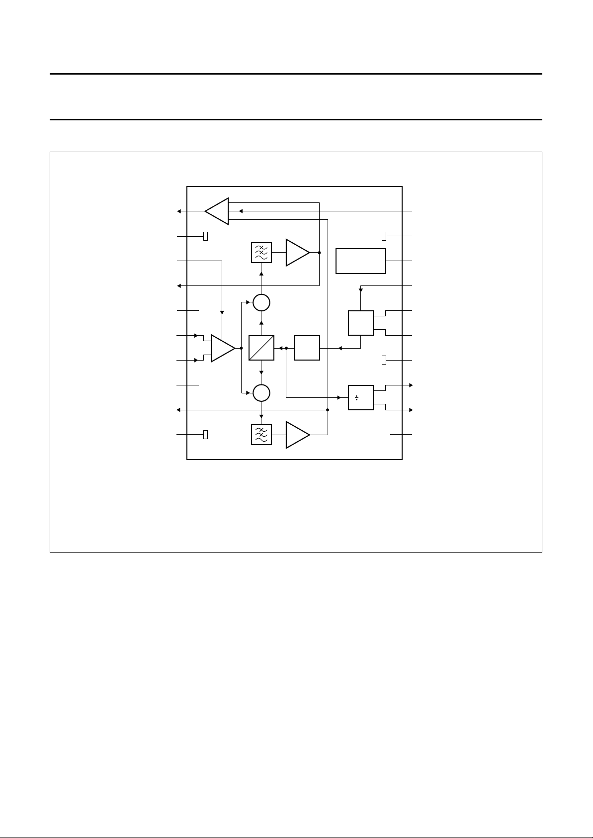
The TDA8042M is a monolitic bipolar IC dedicated for
BPSK and QPSK demodulation. It is designed to be used
together with the TDA8043 as part of a complete
BPSK/QPSK satellite demodulator and decoder.
The bandwidth of the TDA8042M allows symbol rates up
to 45 Msymbols/s. It includes two matched mixers, an IF
gain controlled amplifier, a symmetrical oscillator, a 0°/90°
phase shifter, two low-pass filters and two matched
baseband amplifiers.
The high input sensitivity makes interfacing with various
sources easy. The input sensitivity can be adjusted by
means of an internal AGC amplifier.
The oscillator operates at half the IF frequency. The local
oscillator signal driving the mixers is made by doubling the
oscillator frequency by an internal frequency multiplier.
The oscillator frequency can be set by the appropriate
external LC tank circuit. The internal wideband phase
shifter provides two oscillator signals which are
90 degrees out of phase to drive the mixers.
An AGC detector at the I and Q outputs makes it possible
to keep the I and Q signals at a constant level to drive the
analog-to-digital converters of the TDA8043.
QUICK REFERENCE DATA
SYMBOL PARAMETER CONDITIONS MIN. TYP. MAX. UNIT
V
CC
I
CC
V
i(RF)
f
i(RF)
V
olQ(p-p)
∆E
∆E
∆G
Φ(I-Q)
G(I-Q)
tilt
supply voltage 4.75 5.0 5.25 V
supply current VCC= 5.0 V 54 67.5 81 mA
operating input level − 57 − dBµV
RF input signal frequency 350 − 650 MHz
I and Q output voltage (peak-to-peak value) − 0.8 − V
phase matching error between I and Q channels − 0.7 2 deg
gain matching error between I and Q channels − 0.15 0.8 dB
gain tilt error between I and Q channels − 0.3 0.5 dB
ORDERING INFORMATION
TYPE
NUMBER
NAME DESCRIPTION VERSION
PACKAGE
TDA8042M SSOP20 plastic shrink small outline package; 20 leads; body width 4.4 mm SOT266-1
1997 Apr 11 2
Page 3
Philips Semiconductors Product specification
Quadrature demodulator TDA8042M
BLOCK DIAGRAM
handbook, full pagewidth
IDET
1
DET
20
VTH
IFA
IFB
2
3
4
5
6
7
8
×
0°
90°
×
9
10
I
× 2
Q
VOLTAGE
REFERENCE
VCO
32
GND1
VAGC
IOUT
GND2
V
CC2
QOUT FDIV(B)
GND1
19
GND1
18
V
CC1
17
OSCDIS
16
OSCA
15
OSCB
14
GND1
13
FDIV(A)
12
11
V
CC1
TDA8042M
MBH968
Fig.1 Block diagram.
1997 Apr 11 3
Page 4
Philips Semiconductors Product specification
Quadrature demodulator TDA8042M
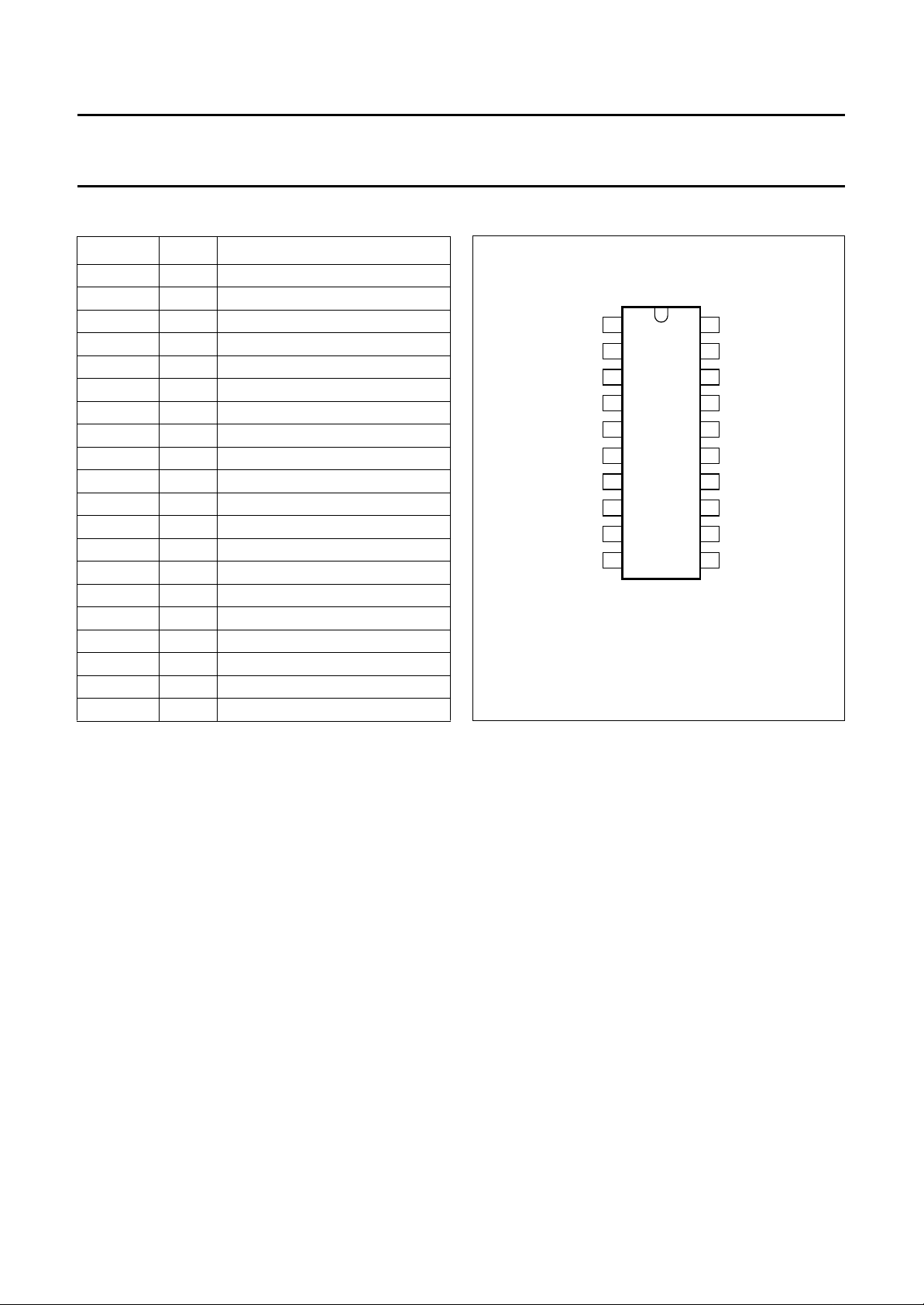
PINNING
SYMBOL PIN DESCRIPTION
IDET 1 AGC detector output signal
GND1 2 ground
VAGC 3 gain control input voltage
IOUT 4 I channel amplifier output
GND2 5 ground
IFA 6 IF input A
IFB 7 IF input B
V
CC2
8 supply voltage 2
QOUT 9 Q channel amplifier output
GND1 10 ground
V
CC1
11 supply voltage 1
FDIV(B) 12 prescaler output B
FDIV(A) 13 prescaler output A
GND1 14 ground
OSCB 15 oscillator tank circuit B
OSCA 16 oscillator tank circuit A
OSCDIS 17 oscillator disable input
V
CC1
18 supply voltage 1
GND1 19 ground
VTH 20 AGC threshold voltage input
handbook, halfpage
IDET VTH
1
GND1 GND1
2
3
VAGC V
IOUT OSCDIS
4
5
GND2 OSCA
IFA OSCB
IFB GND1
V
CC2
QOUT FDIV(B)
GND1 V
TDA8042M
6
7
8
9
10
MBH967
20
19
18
17
16
15
14
13
12
11
CC1
FDIV(A)
CC1
Fig.2 Pin configuration.
1997 Apr 11 4
Page 5

Philips Semiconductors Product specification
Quadrature demodulator TDA8042M
LIMITING VALUES
In accordance with the Absolute Maximum Rating System (IEC 134).
SYMBOL PARAMETER MIN. MAX. UNIT
V
CC
V
i
P
tot
T
stg
T
j
T
amb
Note
1. The operating ambient temperature can be extended up to +85 °C providing the supply voltage remains lower or
equal to 5.2 V in order to maintain the junction temperature below 150 °C.
QUALITY SPECIFICATION
supply voltage −0.3 +6.0 V
input voltage on all pins −0.3 V
CC
V
total power dissipation − 470 mW
IC storage temperature −55 +150 °C
junction temperature − +150 °C
operating ambient temperature 0 +70
(1)
°C
All pins withstand the ESD test in accordance with
“UZW-BO/FQ-B302 (machine model)”
. These numbers can be found in the
“UZW-BO/FQ-A302 (human body model)”
“Quality reference Handbook”
and with
. The handbook
can be ordered using the code 9397 750 00192.
THERMAL CHARACTERISTICS
SYMBOL PARAMETER VALUE UNIT
R
th j-a
thermal resistance from junction to ambient in free air 120 K/W
1997 Apr 11 5
Page 6

Philips Semiconductors Product specification
Quadrature demodulator TDA8042M
CHARACTERISTICS
V
=5V; T
CC
SYMBOL PARAMETER CONDITIONS MIN. TYP. MAX. UNIT
Supply
V
CC1
V
CC2
I
CC1
I
CC2
AGC
G
CR
G
VAGC
R
iVAGC
V
th
R
iVTH
maximum AGC detector output current
I
det
=25°C; R
amb
=1kΩ; measured in application circuit of Fig.4; unless otherwise specified.
L(IQ)
supply voltage 4.75 5.0 5.25 V
supply voltage 4.75 5.0 5.25 V
supply current V
supply current V
CC1=VCC2
CC1=VCC2
=5.0V415161mA
= 5.0 V 13 16.5 20 mA
gain control range 21 29 − dB
voltage gain control at pin 3 note 1
input level = V
input level = V
i(RF)min
i(RF)max
0.5 − 2V
3.5 − 4.5 V
input resistance at pin 3 − 20 − kΩ
AGC threshold voltage note 2
= 1.6 V (peak-to-peak value) − 3.6 − V
V
o
= 0.8 V (peak-to-peak value) − 2.4 − V
V
o
= 0.4 V (peak-to-peak value) − 1.8 − V
V
o
VTH input resistance − 10 − kΩ
note 3 − 1 − mA
(absolute value)
QPSK demodulator
f
i(RF)
R
i(RF)
X
i(RF)
V
i(RF)
∆E
Φ(I-Q)
RF input signal frequency 350 − 650 MHz
RF input impedance (resistive part) f
RF input impedance (reactive part) f
i(RF)
i(RF)
operating RF input level note 1 57 − 78 dBµV
phase matching error between I and Q
note 4 − 0.7 2 deg
channels
∆E
∆G
G(I-Q)
tilt
gain matching error between I and Q channels note 5 − 0.15 0.8 dB
gain tilt error between I and Q channels note 6 − 0.3 0.5 dB
F DSB noise figure source
impedance = 50 Ω;
note 7
d
3(IQ)
third-order intermodulation distortion in I and
note 8 − 50 − dB
Q channels
= 480 MHz − 50 −Ω
= 480 MHz − 19 −Ω
− 13 17 dB
1997 Apr 11 6
Page 7

Philips Semiconductors Product specification
Quadrature demodulator TDA8042M
SYMBOL PARAMETER CONDITIONS MIN. TYP. MAX. UNIT
Oscillator
f
osc
∆f
osc
N
osc
V
osc(dis)
Prescaler
V
OH
V
OL
δ output duty cycle 40 50 60 %
DIV
spu(IQ)
I and Q internal filters
B
−1
B
−30
I and Q output amplifiers
V
O(IQ)(DC)
V
o(IQ)(p-p)
V
clip(p-p)
R
L(IQ)
R
o(IQ)
α
ct(I-Q)
Notes
1. The voltage gain control range (G
800 mV (peak-to-peak value) at I and Q outputs.
The lowest control voltage corresponds to the highest sensitivity and gain.
2. Vth is the level of voltage to be applied at pin 20 to get a current I
amplitude of the signal at I and Q outputs.
The AGC threshold voltage can be set by a resistive voltage divider connected at pin 20. Without the external
resistors Vthis set at a value close to 2.35 V.
3. The current I
Vth.
4. The phase error is defined as the phase quadrature imbalance between I and Q channels.
5. The gain error is defined as the phase quadrature imbalance between I and Q channels.
6. The tilt is defined as the difference between the maximum and the minimum channel gain measured in a frequency
band of ±30 MHz around f
oscillator frequency note 9 175 − 325 MHz
frequency drift note 10 −−500 kHz
= ±5% −−100 kHz
∆V
CC
oscillator phase noise measured10 kHz
from f
; note 11
osc
−−91 dBc/Hz
oscillator disable voltage at pin 17
oscillator disabled −−1.0 V
oscillator enabled 4.0 −−V
HIGH level output voltage note 12 4.0 −−V
LOW level output voltage note 12 −−3.35 V
output spurious voltage at I and Q outputs note 13 −−50 − dB
bandwidth for 1 dB attenuation 30 −−MHz
bandwidth for 30 dB attenuation − 450 − MHz
I and Q channels DC output voltage − 2.45 − V
I and Q channels output voltage
note 14 − 0.8 − V
(peak-to-peak value)
I and Q output clipping level
1.8 V
(peak-to-peak value)
I and Q channels output load resistance note 15 500 −−Ω
I and Q channels output resistance − 67 −Ω
crosstalk between I and Q channels 30 −−dB
) is defined as the DC voltage to be applied on pin 3 to get a signal level of
VAGC
of 0.5 mA at pin 1. This voltage depends on the
det
increases when the output level (at pins 4 and 9) increases above the value set by the adjustment of
det
. The specified tilt is the maximum tilt value found in one of the I and Q channels.
i(RF)
1997 Apr 11 7
Page 8

Philips Semiconductors Product specification
Quadrature demodulator TDA8042M
7. The specified noise figure is the maximum value obtained from I and Q channels noise measurement. The figure
holds for the maximum gain (G
8. The specified intermodulation distortion is the minimum value obtained from intermodulation measurements in I and
Q channels. The specified value is the minimum distance between wanted signal and intermodulation products
measured at the output for a wanted output level of 0.8 V (peak-to-peak value).
9. The oscillator is tuned with an appropriate tank circuit designed for each frequency limit.
10. The drift of the oscillator frequency with temperature is defined for ∆T
circuit (see Fig.4) with a temperature compensated tank circuit. The temperature compensation used for this
measurement is realized using the application which is depicted in Fig.3.
11. The phase noise is measured at the oscillator frequency (= 240 MHz). Due to the internal frequency doubler the
phase noise at the input of the mixers will be 6 dB worse.
12. Measured with a high impedance load (RL>5kΩ) connected at pins 12 and 13.
13. The prescaler output spurious voltage at I and Q outputs are measured with respect to an output level of 800 mV
(peak-to-peak value).
14. Measured with an input signal f
15. The load should be AC-coupled.
= 0.5 V).
VAGC
+ 500 kHz (i.e. 480.5 MHz).
i(RF)
=25°C. It is measured in the application
amb
handbook, full pagewidth
to pin 15
TOKO ref.:
100 082 93278
to pin 16
8.2 pF
NP0
2.2 pF
NP0
Fig.3 Temperature compensation circuit.
6 pF
N470
1 pF
N470
MBH969
1997 Apr 11 8
Page 9

Philips Semiconductors Product specification
Quadrature demodulator TDA8042M
APPLICATION INFORMATION
handbook, full pagewidth
NOT ON THE TESTBOARD
50 Ω
RF
5 V
1 kΩ
H-183-4
test point
ANZAC
5 V
100 nF
100 nF
100
nF
100
nF
100
nF
1 kΩ
1 kΩ
5 kΩ
10 nF
10 nF
5 V
GND1
VAGC
GND2
V
QOUT
GND1
IDET
IOUT
IFA
IFB
CC2
1
2
3
4
5
6
7
8
9
TDA8042M
20
19
18
17
16
15
14
13
12
1110
MBH970
VTH
100
nF
GND1
V
CC1
OSCDIS
OSCA
18 pF
OSCB
GND1
FDIV(A)
FDIV(B)
V
CC1
10 nF
10 nF
1 kΩ
100
nF
100
nF
470 Ω
470 Ω
100
nF
+
5 V
TOKO ref.:
100 082 93278
5 V
5 V
maximum
to
prescaler
Fig.4 Application diagram.
1997 Apr 11 9
Page 10

Philips Semiconductors Product specification
Quadrature demodulator TDA8042M
PACKAGE OUTLINE
SSOP20: plastic shrink small outline package; 20 leads; body width 4.4 mm
D
c
y
Z
20
pin 1 index
11
A
2
A
1
110
w M
b
e
p
E
H
E
detail X
SOT266-1
A
X
v M
A
Q
(A )
L
p
L
A
3
θ
0 2.5 5 mm
scale
DIMENSIONS (mm are the original dimensions)
mm
OUTLINE
VERSION
SOT266-1
A
max.
1.5
0.1501.4
1.2
b
3
p
0.32
0.20
0.20
0.13
0.25
IEC JEDEC EIAJ
UNIT A1A2A
Note
1. Plastic or metal protrusions of 0.20 mm maximum per side are not included.
(1)E(1)
cD
6.6
6.4
REFERENCES
4.5
0.65 1.0 0.2
4.3
1997 Apr 11 10
eHELLpQZywv θ
6.6
6.2
0.75
0.45
0.65
0.45
PROJECTION
0.13 0.1
EUROPEAN
(1)
0.48
0.18
ISSUE DATE
90-04-05
95-02-25
o
10
o
0
Page 11

Philips Semiconductors Product specification
Quadrature demodulator TDA8042M
SOLDERING
Introduction
There is no soldering method that is ideal for all IC
packages. Wave soldering is often preferred when
through-hole and surface mounted components are mixed
on one printed-circuit board. However, wave soldering is
not always suitable for surface mounted ICs, or for
printed-circuits with high population densities. In these
situations reflow soldering is often used.
This text gives a very brief insight to a complex technology.
A more in-depth account of soldering ICs can be found in
our
“IC Package Databook”
Reflow soldering
Reflow soldering techniques are suitable for all SSOP
packages.
Reflow soldering requires solder paste (a suspension of
fine solder particles, flux and binding agent) to be applied
to the printed-circuit board by screen printing, stencilling or
pressure-syringe dispensing before package placement.
Several techniques exist for reflowing; for example,
thermal conduction by heated belt. Dwell times vary
between 50 and 300 seconds depending on heating
method. Typical reflow temperatures range from
215 to 250 °C.
Preheating is necessary to dry the paste and evaporate
the binding agent. Preheating duration: 45 minutes at
45 °C.
Wave soldering
Wave soldering isnot recommended for SSOP packages.
This is because of the likelihood of solder bridging due to
closely-spaced leads and the possibility of incomplete
solder penetration in multi-lead devices.
(order code 9398 652 90011).
If wave soldering cannot be avoided, the following
conditions must be observed:
• A double-wave (a turbulent wave with high upward
pressure followed by a smooth laminar wave)
soldering technique should be used.
• The longitudinal axis of the package footprint must
be parallel to the solder flow and must incorporate
solder thieves at the downstream end.
Even with these conditions, only consider wave
soldering SSOP packages that have a body width of
4.4 mm, that is SSOP16 (SOT369-1) or
SSOP20 (SOT266-1).
During placement and before soldering, the package must
be fixed with a droplet of adhesive. The adhesive can be
applied by screen printing, pin transfer or syringe
dispensing. The package can be soldered after the
adhesive is cured.
Maximum permissible solder temperature is 260 °C, and
maximum duration of package immersion in solder is
10 seconds, if cooled to less than 150 °C within
6 seconds. Typical dwell time is 4 seconds at 250 °C.
A mildly-activated flux will eliminate the need for removal
of corrosive residues in most applications.
Repairing soldered joints
Fix the component by first soldering two diagonallyopposite end leads. Use only a low voltage soldering iron
(less than 24 V) applied to the flat part of the lead. Contact
time must be limited to 10 seconds at up to 300 °C. When
using a dedicated tool, all other leads can be soldered in
one operation within 2 to 5 seconds between
270 and 320 °C.
1997 Apr 11 11
Page 12

Philips Semiconductors Product specification
Quadrature demodulator TDA8042M
DEFINITIONS
Data sheet status
Objective specification This data sheet contains target or goal specifications for product development.
Preliminary specification This data sheet contains preliminary data; supplementary data may be published later.
Product specification This data sheet contains final product specifications.
Limiting values
Limiting values given are in accordance with the Absolute Maximum Rating System (IEC 134). Stress above one or
more of the limiting values may cause permanent damage to the device. These are stress ratings only and operation
of the device at these or at any other conditions above those given in the Characteristics sections of the specification
is not implied. Exposure to limiting values for extended periods may affect device reliability.
Application information
Where application information is given, it is advisory and does not form part of the specification.
LIFE SUPPORT APPLICATIONS
These products are not designed for use in life support appliances, devices, or systems where malfunction of these
products can reasonably be expected to result in personal injury. Philips customers using or selling these products for
use in such applications do so at their own risk and agree to fully indemnify Philips for any damages resulting from such
improper use or sale.
1997 Apr 11 12
Page 13

Philips Semiconductors Product specification
Quadrature demodulator TDA8042M
NOTES
1997 Apr 11 13
Page 14

Philips Semiconductors Product specification
Quadrature demodulator TDA8042M
NOTES
1997 Apr 11 14
Page 15

Philips Semiconductors Product specification
Quadrature demodulator TDA8042M
NOTES
1997 Apr 11 15
Page 16

Philips Semiconductors – a worldwide company
Argentina: see South America
Australia: 34 Waterloo Road, NORTH RYDE, NSW 2113,
Tel. +61 2 9805 4455, Fax. +61 29805 4466
Austria: Computerstr. 6, A-1101 WIEN, P.O. Box 213,
Tel. +43 1 60 101, Fax. +43 1 60 101 1210
Belarus: Hotel Minsk Business Center, Bld. 3, r. 1211, Volodarski Str.6,
220050 MINSK, Tel. +375 172 200 733, Fax. +375 172 200773
Belgium: see The Netherlands
Brazil: see South America
Bulgaria: Philips Bulgaria Ltd., Energoproject, 15th floor,
51 James Bourchier Blvd., 1407 SOFIA,
Tel. +359 2 689 211, Fax. +359 2689 102
Canada: PHILIPS SEMICONDUCTORS/COMPONENTS,
Tel. +1 800 234 7381
China/Hong Kong: 501 Hong Kong Industrial Technology Centre,
72 Tat Chee Avenue, Kowloon Tong, HONG KONG,
Tel. +852 2319 7888, Fax. +8522319 7700
Colombia: see South America
Czech Republic: see Austria
Denmark: Prags Boulevard 80, PB 1919, DK-2300 COPENHAGEN S,
Tel. +45 32 88 2636, Fax. +45 31 57 0044
Finland: Sinikalliontie 3, FIN-02630 ESPOO,
Tel. +358 9 615800, Fax. +358 9 61580920
France: 4 Rue du Port-aux-Vins, BP317, 92156 SURESNES Cedex,
Tel. +33 1 40 99 6161, Fax. +33 1 4099 6427
Germany: Hammerbrookstraße 69, D-20097 HAMBURG,
Tel. +49 40 23 53 60, Fax. +4940 23536 300
Greece: No. 15, 25th March Street, GR 17778 TAVROS/ATHENS,
Tel. +30 1 4894 339/239, Fax. +30 14814 240
Hungary: see Austria
India: Philips INDIA Ltd, Shivsagar Estate, A Block, Dr. Annie Besant Rd.
Worli, MUMBAI 400 018, Tel. +91 22 4938541, Fax.+91 224938 722
Indonesia: see Singapore
Ireland: Newstead, Clonskeagh, DUBLIN 14,
Tel. +353 1 7640 000, Fax.+353 17640 200
Israel: RAPAC Electronics, 7 Kehilat Saloniki St, PO Box 18053,
TEL AVIV 61180, Tel. +9723 6450444, Fax.+972 3649 1007
Italy: PHILIPS SEMICONDUCTORS, Piazza IV Novembre 3,
20124 MILANO, Tel. +39 2 6752 2531, Fax. +392 67522557
Japan: Philips Bldg 13-37, Kohnan 2-chome, Minato-ku, TOKYO 108,
Tel. +81 3 3740 5130, Fax. +81 33740 5077
Korea: Philips House, 260-199 Itaewon-dong, Yongsan-ku, SEOUL,
Tel. +82 2 709 1412, Fax. +82 2 709 1415
Malaysia: No. 76 Jalan Universiti, 46200 PETALING JAYA, SELANGOR,
Tel. +60 3 750 5214, Fax. +603 7574880
Mexico: 5900 Gateway East, Suite 200, EL PASO, TEXAS 79905,
Tel. +9-5 800 234 7381
Middle East: see Italy
Netherlands: Postbus 90050, 5600PB EINDHOVEN, Bldg. VB,
Tel. +31 40 27 82785, Fax.+31 4027 88399
New Zealand: 2 Wagener Place, C.P.O. Box 1041, AUCKLAND,
Tel. +64 9 849 4160, Fax. +64 9 849 7811
Norway: Box 1, Manglerud 0612, OSLO,
Tel. +47 22 74 8000, Fax. +47 22 74 8341
Philippines: Philips Semiconductors Philippines Inc.,
106 Valero St. Salcedo Village, P.O. Box2108 MCC,MAKATI,
Metro MANILA, Tel. +63 2 816 6380, Fax. +632 817 3474
Poland: Ul. Lukiska 10, PL 04-123 WARSZAWA,
Tel. +48 22 612 2831, Fax.+48 22612 2327
Portugal: see Spain
Romania: see Italy
Russia: Philips Russia, Ul. Usatcheva 35A, 119048 MOSCOW,
Tel. +7 095 755 6918, Fax.+7 095755 6919
Singapore: Lorong 1, Toa Payoh, SINGAPORE 1231,
Tel. +65 350 2538, Fax. +65 251 6500
Slovakia: see Austria
Slovenia: see Italy
South Africa: S.A. PHILIPS Pty Ltd., 195-215 Main Road Martindale,
2092 JOHANNESBURG, P.O. Box 7430 Johannesburg 2000,
Tel. +27 11 470 5911, Fax.+27 11470 5494
South America: Rua do Rocio 220, 5th floor, Suite 51,
04552-903 São Paulo, SÃO PAULO - SP, Brazil,
Tel. +55 11 821 2333, Fax.+55 11829 1849
Spain: Balmes 22, 08007 BARCELONA,
Tel. +34 3 301 6312, Fax. +34 3 301 4107
Sweden: Kottbygatan 7, Akalla, S-16485 STOCKHOLM,
Tel. +46 8 632 2000, Fax. +46 8 632 2745
Switzerland: Allmendstrasse 140, CH-8027 ZÜRICH,
Tel. +41 1 488 2686, Fax. +41 1 481 7730
Taiwan: Philips Semiconductors, 6F, No. 96, Chien Kuo N. Rd., Sec. 1,
TAIPEI, Taiwan Tel. +886 2 2134 2865, Fax. +886 22134 2874
Thailand: PHILIPS ELECTRONICS (THAILAND) Ltd.,
209/2 Sanpavuth-Bangna Road Prakanong, BANGKOK 10260,
Tel. +66 2 745 4090, Fax. +66 2 398 0793
Turkey: Talatpasa Cad. No. 5, 80640 GÜLTEPE/ISTANBUL,
Tel. +90 212 279 2770, Fax. +90 212 282 6707
Ukraine: PHILIPS UKRAINE, 4 Patrice Lumumba str., Building B, Floor 7,
252042 KIEV, Tel. +380 44 264 2776, Fax. +38044 2680461
United Kingdom: Philips Semiconductors Ltd., 276 Bath Road, Hayes,
MIDDLESEX UB3 5BX, Tel. +44 181 730 5000, Fax.+44 181754 8421
United States: 811 East Arques Avenue, SUNNYVALE, CA 94088-3409,
Tel. +1 800 234 7381
Uruguay: see South America
Vietnam: see Singapore
Yugoslavia: PHILIPS, Trg N. Pasica 5/v, 11000 BEOGRAD,
Tel. +381 11 625 344, Fax.+38111 635777
For all other countries apply to: Philips Semiconductors, Marketing & Sales Communications,
Building BE-p, P.O. Box 218, 5600 MD EINDHOVEN, TheNetherlands, Fax.+31 4027 24825
© Philips Electronics N.V. 1997 SCA54
All rights are reserved. Reproduction in whole or in part is prohibited without the prior written consent of the copyright owner.
The information presented in this document does not form part of any quotation or contract, is believed to be accurate and reliable and may be changed
without notice. No liability will be accepted by the publisher for any consequence of its use. Publication thereof does not convey nor imply any license
under patent- or other industrial or intellectual property rights.
Internet: http://www.semiconductors.philips.com
Printed in The Netherlands 547047/1200/01/pp16 Date of release: 1997 Apr 11 Document order number: 9397 750 00909
 Loading...