

Page 1

DATA SH EET
Objective specification
Supersedes data of 1996 Oct 08
File under Integrated Circuits, IC02
1996 Oct 24
INTEGRATED CIRCUITS
TDA8010M; TDA8010AM
Low power mixers/oscillators
for satellite tuners
Page 2

1996 Oct 24 2
Philips Semiconductors Objective specification
Low power mixers/oscillators
for satellite tuners
TDA8010M;
TDA8010AM
FEATURES
• Fully balanced mixer with common base input
• Wide input power and frequency range
• One-band 2 pin oscillator
• Local oscillator buffer and prescaler
• SAW filter IF preamplifier with gain control input and
switchable output
• Bandgap voltage stabilizer for oscillator stability
• External IF filter between the mixer output and the IF
amplifier input.
APPLICATIONS
• Down frequency conversion in DBS (Direct
Broadcasting Satellite) satellite receivers.
GENERAL DESCRIPTION
The TDA8010M; TDA8010AM are integrated circuits that
perform the mixer/oscillator function in satellite tuners.
The devices include a gain controlled IF amplifier that can
directly drive two single-ended SAW filters or a differential
SAW filter using a three function switchable output.
They contain an internal LO prescaler and buffer that is
compatible with the input of a terrestrial or satellite
frequency synthesizer. They are also suitable for digital TV
tuners. These devices are available in small outline
packages that give the designer the capability to design an
economical and physically small satellite tuner.
QUICK REFERENCE DATA
ORDERING INFORMATION
SYMBOL PARAMETER CONDITIONS MIN. TYP. MAX. UNIT
V
CC
supply voltage 4.5 5.0 5.5 V
I
CC
supply current − 70 − mA
f
RF
RF frequency range 700 − 2150 MHz
f
osc
oscillator frequency 1380 − 2650 MHz
NF
M
mixer noise figure corrected for image − 10 − dB
G
max
maximum total gain mixer plus IF − 40 − dB
G
min
minimum total gain mixer plus IF −−17 − dB
TYPE
NUMBER
PACKAGE
NAME DESCRIPTION VERSION
TDA8010M
SSOP20 plastic shrink small outline package; 20 leads; body width 4.4 mm SOT266-1
TDA8010AM
Page 3
1996 Oct 24 3
Philips Semiconductors Objective specification
Low power mixers/oscillators
for satellite tuners
TDA8010M; TDA8010AM
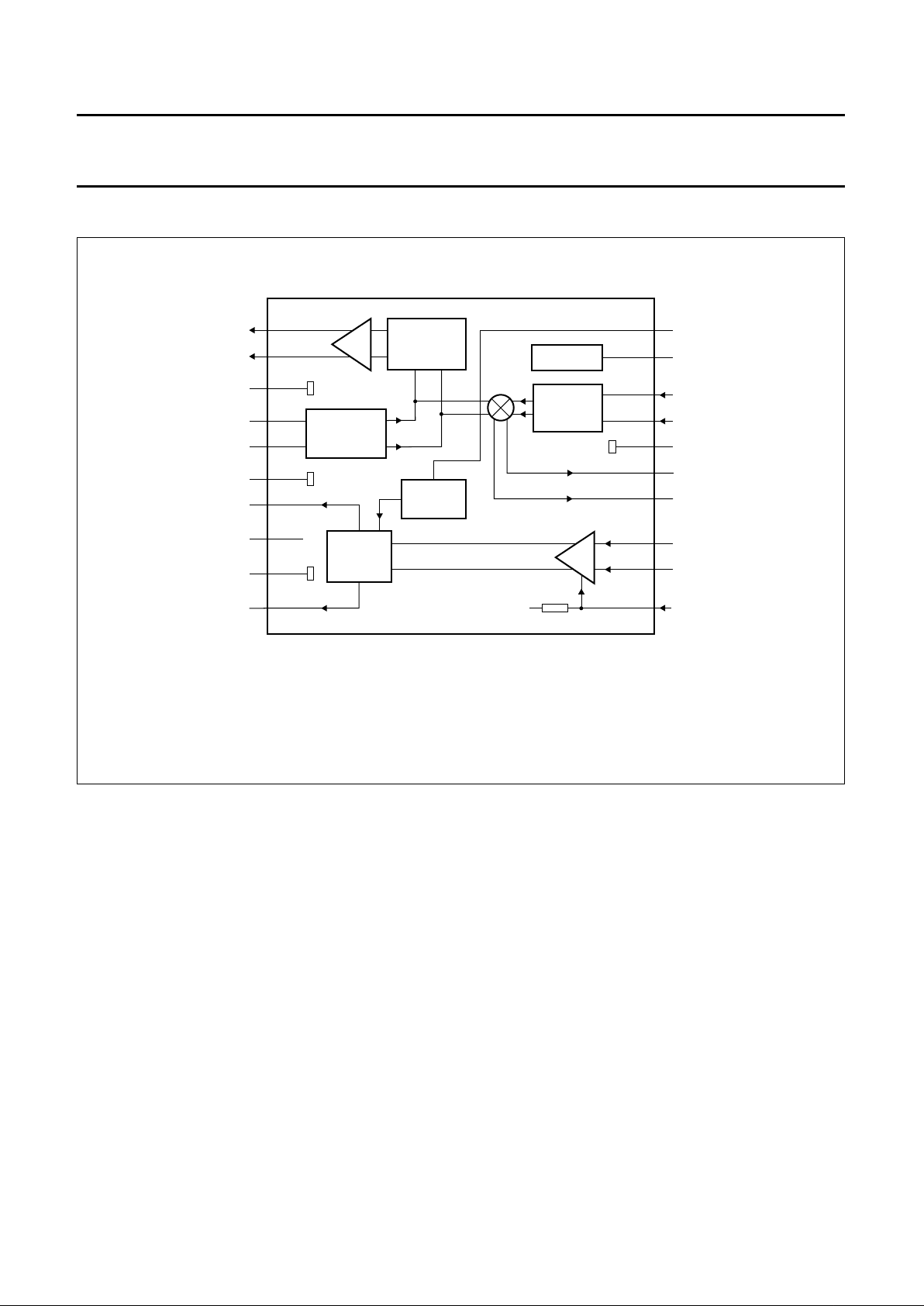
BLOCK DIAGRAM
Fig.1 Block diagram.
handbook, full pagewidth
MGE506
DIVIDE-BY-2
PRE-SCALER
OSCILLATOR
STABILIZER
RF INPUT
STAGE
SWITCH
CONTROL
LO
BUFFER
IF AMP
OUTPUT
SWITCH
V
CC
20 (1)
19 (2)
18 (3)
17 (4)
16 (5)
15 (6)
14 (7)
13 (8)
12 (9)
11 (10)
(11) 10
(12) 9
(13) 8
(14) 7
(15) 6
(16) 5
(17) 4
(18) 3
(19) 2
(20) 1
LOOUT2
LOOUT1
LOGND
OSC2
OSC1
OSCGND
IFOUT2
V
CC
IFGND
IFOUT1
AGC
IFIN2
IFIN1
MOUT2
MOUT1
RFIN1
MGND
RFIN2
V
CCM
SC
TDA8010M
TDA8010AM
R
AGC
The pin numbers given in parenthesis refer to the TDA8010AM.
Page 4
1996 Oct 24 4
Philips Semiconductors Objective specification
Low power mixers/oscillators
for satellite tuners
TDA8010M; TDA8010AM
PINNING
SYMBOL
PINS
DESCRIPTION
TDA8010M TDA8010AM
SC 1 20 IF output switch control
V
CCM
2 19 supply voltage for mixer
RFIN1 3 18 RF input 1
RFIN2 4 17 RF input 2
MGND 5 16 ground for mixer
MOUT1 6 15 mixer output 1
MOUT2 7 14 mixer output 2
IFIN1 8 13 IF amplifier input 1
IFIN2 9 12 IF amplifier input 2
AGC 10 11 IF amplifier gain control input
IFOUT1 11 10 IF amplifier output 1
IFGND 12 9 ground for IF amplifier
V
CC
13 8 supply voltage
IFOUT2 14 7 IF amplifier output 2
OSCGND 15 6 ground for oscillator
OSC1 16 5 oscillator tuning circuit input 1
OSC2 17 4 oscillator tuning circuit input 2
LOGND 18 3 ground for local oscillator buffer
LOOUT1 19 2 local oscillator output 1
LOOUT2 20 1 local oscillator output 2
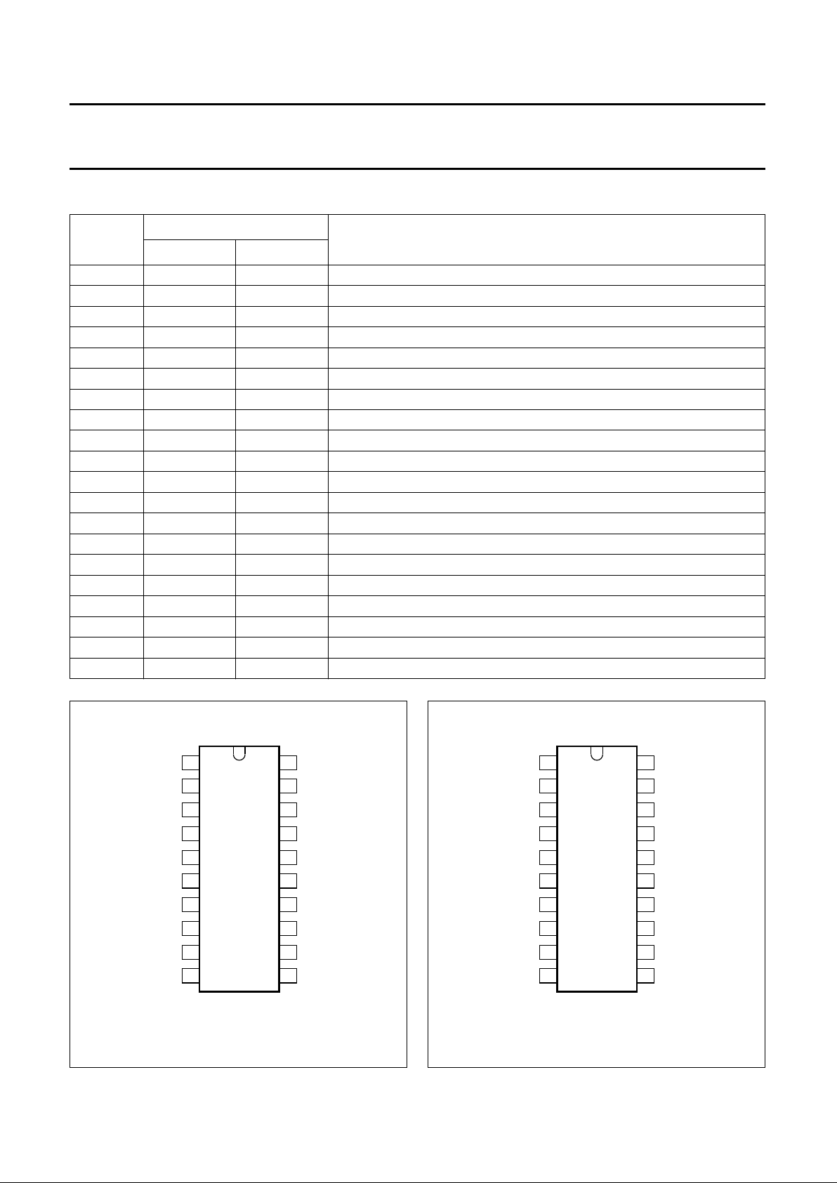
Fig.2 Pin configuration (TDA8010M).
handbook, halfpage
SC
V
CCM
RFIN1
RFIN2
MGND
MOUT1
MOUT2
IFIN1
IFIN2
AGC
LOOUT2
LOOUT1
LOGND
OSC2
OSCGND
IFOUT2
OSC1
V
CC
IFGND
IFOUT1
1
2
3
4
5
6
7
8
9
10
11
12
20
19
18
17
16
15
14
13
TDA8010M
MGE504
Fig.3 Pin configuration (TDA8010AM).
handbook, halfpage
LOOUT2
LOOUT1
LOGND
OSC2
OSC1
OSCGND
IFOUT2
V
CC
IFGND
IFOUT1
SC
V
CCM
RFIN1
RFIN2
MOUT1
MOUT2
MGND
IFIN1
IFIN2
AGC
1
2
3
4
5
6
7
8
9
10
11
12
20
19
18
17
16
15
14
13
TDA8010AM
MGE505
Page 5

1996 Oct 24 5
Philips Semiconductors Objective specification
Low power mixers/oscillators
for satellite tuners
TDA8010M; TDA8010AM
LIMITING VALUES
In accordance with the Absolute Maximum Rating System (IEC 134).
THERMAL CHARACTERISTICS
HANDLING
All pins withstand the ESD test in accordance with
“UZW-BO/FQ-A302 (human body model)”
and with
“UZW-BO/FQ-B302 (machine model)”
.
SYMBOL PARAMETER MIN. MAX. UNIT
V
CC
supply voltage −0.3 +6.0 V
V
i(max)
maximum input voltage on all pins −0.3 V
CC
V
I
source(max)
maximum output source current − 10 mA
t
sc
maximum short-circuit time on all outputs − 10 s
T
stg
storage temperature −55 +150 °C
T
j
junction temperature − 150 °C
T
amb
operating ambient temperature −20 +80 °C
SYMBOL PARAMETER VALUE UNIT
R
th j-a
thermal resistance from junction to ambient in free air 120 K/W
Page 6

1996 Oct 24 6
Philips Semiconductors Objective specification
Low power mixers/oscillators
for satellite tuners
TDA8010M; TDA8010AM
CHARACTERISTICS
VCC=5V; T
amb
=25°C; measured in application circuit of Fig.6; unless otherwise specified.
SYMBOL PARAMETER CONDITIONS MIN. TYP. MAX. UNIT
Supplies
V
CC
supply voltage 4.75 5.0 5.25 V
I
CC
supply current 60 70 80 mA
Mixer
f
RF
RF frequency range 700 − 2150 MHz
NF total noise figure (mixer plus IF);
not corrected for image
V
AGC
= 0.9VCC; fi= 920 MHz − 810dB
V
AGC
= 0.9VCC; fi= 2150 MHz − 13 15 dB
G
M
available power gain for mixer RL= 2.2 kΩ−10 − dB
G
max1
maximum total gain
(mixer + IFOUT1)
fi= 920 MHz; notes 1 and 2 37 40 − dB
f
i
= 2150 MHz; notes 1 and 2 36 38 − dB
G
min1
minimum total gain
(mixer + IFOUT1)
notes 1 and 2 −−30 −14 dB
G
max2
maximum total gain
(mixer + IFOUT2)
fi= 920 MHz; notes 1 and 2 36 39 − dB
f
i
= 2150 MHz; notes 1 and 2 35 37 − dB
G
min2
minimum total gain
(mixer + IFOUT2)
notes 1 and 2 −−30 −15 dB
Z
I(RF)
input impedance (Rs+Ls) from 920 to 2150 MHz 20 30 40 Ω
5 7.5 10 nH
Z
O(RF)
output impedance (Rp//Cp)
(open collector)
fIF= 480 MHz 8 12 16 kΩ
450 550 650 fF
IP3 third-order interception point see Fig.4 −2+2− dBm
IP2 second-order interception point see Fig.5 10 25 − dBm
Local oscillator output
V
LO
output voltage RL=50Ω 87 90 93 dBµV
SRF spurious signal on LO output
with respect to LO output signal
R
L
=50Ω; note 3 −−35 −10 dB
LO
leak
local oscillator leakage RF input −−50 − dBm
IF output (mixer) −−35 − dBm
Oscillator
f
osc
oscillator frequency range VCC= 4.5 to 5.5 V;
T
amb
= −20 to +80 °C
1380 − 2650 MHz
f
osc(max)
maximum oscillator frequency − 2700 − MHz
f
shift
oscillator frequency shift VCC= 4.75 to 5.25 V;
at 2550 MHz
−±350 ±500 kHz
V
CC
= 4.75 to 5.25 V;
at 2650 MHz
−±400 ±600 kHz
f
drift
oscillator frequency drift ∆T=25°C; at 2550 MHz −−8−15 MHz
∆T=25°C;at 2650 MHz −−8−16 MHz
Page 7

1996 Oct 24 7
Philips Semiconductors Objective specification
Low power mixers/oscillators
for satellite tuners
TDA8010M; TDA8010AM
Notes
1. Maximum gain: V
AGC
= 0.9VCC; fIF= 480 MHz; IF output single-ended.
2. Minimum gain: V
AGC
= 0.1VCC; fIF= 480 MHz; IF output single-ended.
3. RF input power range = −70 to −20 dBm.
4. V
AGC
= 0.9VCC; fIF= 480 MHz; R
source
= 100 Ω.
5. Switch isolation is defined at an IF output level of 77 dBµV; fIF= 480 MHz.
ΦN oscillator phase noise at 100 kHz 88 92 − dBc
at 10 kHz 62 69 − dBc
IF amplifier
f
IF
IF frequency range 60 − 625 MHz
G
v(max)
maximum voltage gain note 1 − 40 − dB
G
v(min)
minimum voltage gain note 2 −−30 − dB
NF
IF
IF noise figure note 4 − 8 − dB
V
oIF
output voltage level −−85 dBµV
Z
O(IF)
output impedance single-ended − 50 −Ω
Z
I(IF)
input impedance (Rp//Lp) 303336 Ω
579 nH
SW
iso
switch isolation note 5 33 36 − dB
V
SW
switch control voltage IF1 on; IF2 off 0.8V
CC
− V
CC
V
IF1 off; IF2 on 0.2V
CC
− 0.6V
CC
V
differential output 0 − 0.07V
CC
V
R
I(AGC)
AGC input resistance see Fig.6 − 4 − kΩ
SYMBOL PARAMETER CONDITIONS MIN. TYP. MAX. UNIT
Fig.4 IP3 measurement method.
REF is the level if F1 or F2 were at 480 MHz.
IP3 = IM3/2 + input level.
Input level: 2 ×−23 dBm.
Output level: 2 × 74 dBµV.
handbook, halfpage
MGE507
2F1 − F2 F1 F2 2F2 − F1
390 420 450 480 (MHz)
IM3
REF
Fig.5 IP2 measurement method.
IP2 = IM2 + input level.
Input level: 2 ×−23 dBm.
Output level: 2 × 74 dBµV.
handbook, halfpage
MGE508
LO − F1 LO − F2 (F1 + F2) − LO
FIRF478 480 484 (MHz)
964 962 1926 (MHz)
IM2
Page 8

1996 Oct 24 8
Philips Semiconductors Objective specification
Low power mixers/oscillators
for satellite tuners
TDA8010M; TDA8010AM
APPLICATION INFORMATION
ook, full pagewidth
MGE509
DIVIDE-BY-2
PRE-SCALER
OSCILLATOR
STABILIZER
RF INPUT
STAGE
SWITCH
CONTROL
LO
BUFFER
IF AMP
OUTPUT
SWITCH
V
CC
1
2
3
4
5
6
7
8
9
10
11
12
13
14
15
16
17
18
19
20
SC
V
CCM
RFIN1
RFIN2
MGND
MOUT1
MOUT2
IFIN1
IFIN2
AGC
IFOUT1
IFGND
V
CC
IFOUT2
OSCGND
LOGND
OSC1
OSC2
LOOUT1
LOOUT2
TDA8010AM
R
AGC
3.3 nF
150
Ω
3.3 nF
150
Ω
10
nF
V
CC
22 kΩ
22 kΩ
22 kΩ
22 kΩ
1.5 pF
L3
L3
BB833
BB833
1 nF
12
kΩ
12
kΩ
2.2
µF
VT
3.3 nF
3.3 nF
50 Ω load
10
nF
3.3 pF
2.7
pF
2.7
pF
3.3 pF
L2
3.3 kΩ
V
CC
33 Ω
L1
0.56 pF
3.3 nF
3.3 nF
V
CC
10 nF
Fig.6 Application diagram.
L1: 5.5 turns; diameter = 5 mm.
L2: 5.5 turns; diameter = 1.5 mm.
L3: micro-strip coil; L = 3.5 × 0.4 mm. No ground plane on the other side.
Varicaps: Siemens BB833.
Page 9

1996 Oct 24 9
Philips Semiconductors Objective specification
Low power mixers/oscillators
for satellite tuners
TDA8010M; TDA8010AM
PACKAGE OUTLINE
UNIT A1A2A
3
b
p
cD
(1)E(1)
(1)
eHELLpQZywv θ
REFERENCES
OUTLINE
VERSION
EUROPEAN
PROJECTION
ISSUE DATE
IEC JEDEC EIAJ
mm
0.1501.4
1.2
0.32
0.20
0.20
0.13
6.6
6.4
4.5
4.3
0.65 1.0 0.2
6.6
6.2
0.65
0.45
0.48
0.18
10
0
o
o
0.13 0.1
DIMENSIONS (mm are the original dimensions)
Note
1. Plastic or metal protrusions of 0.20 mm maximum per side are not included.
0.75
0.45
SOT266-1
90-04-05
95-02-25
w M
θ
A
A
1
A
2
b
p
D
H
E
L
p
Q
detail X
E
Z
e
c
L
v M
A
X
(A )
3
A
y
0.25
110
20
11
pin 1 index
0 2.5 5 mm
scale
SSOP20: plastic shrink small outline package; 20 leads; body width 4.4 mm
SOT266-1
A
max.
1.5
Page 10

1996 Oct 24 10
Philips Semiconductors Objective specification
Low power mixers/oscillators
for satellite tuners
TDA8010M; TDA8010AM
SOLDERING
Introduction
There is no soldering method that is ideal for all IC
packages. Wave soldering is often preferred when
through-hole and surface mounted components are mixed
on one printed-circuit board. However, wave soldering is
not always suitable for surface mounted ICs, or for
printed-circuits with high population densities. In these
situations reflow soldering is often used.
This text gives a very brief insight to a complex technology.
A more in-depth account of soldering ICs can be found in
our
“IC Package Databook”
(order code 9398 652 90011).
Reflow soldering
Reflow soldering techniques are suitable for all SSOP
packages.
Reflow soldering requires solder paste (a suspension of
fine solder particles, flux and binding agent) to be applied
to the printed-circuit board by screen printing, stencilling or
pressure-syringe dispensing before package placement.
Several techniques exist for reflowing; for example,
thermal conduction by heated belt. Dwell times vary
between 50 and 300 seconds depending on heating
method. Typical reflow temperatures range from
215 to 250 °C.
Preheating is necessary to dry the paste and evaporate
the binding agent. Preheating duration: 45 minutes at
45 °C.
Wave soldering
Wave soldering isnot recommended for SSOP packages.
This is because of the likelihood of solder bridging due to
closely-spaced leads and the possibility of incomplete
solder penetration in multi-lead devices.
If wave soldering cannot be avoided, the following
conditions must be observed:
• A double-wave (a turbulent wave with high upward
pressure followed by a smooth laminar wave)
soldering technique should be used.
• The longitudinal axis of the package footprint must
be parallel to the solder flow and must incorporate
solder thieves at the downstream end.
Even with these conditions, only consider wave
soldering SSOP packages that have a body width of
4.4 mm, that is SSOP16 (SOT369-1) or
SSOP20 (SOT266-1).
During placement and before soldering, the package must
be fixed with a droplet of adhesive. The adhesive can be
applied by screen printing, pin transfer or syringe
dispensing. The package can be soldered after the
adhesive is cured.
Maximum permissible solder temperature is 260 °C, and
maximum duration of package immersion in solder is
10 seconds, if cooled to less than 150 °C within
6 seconds. Typical dwell time is 4 seconds at 250 °C.
A mildly-activated flux will eliminate the need for removal
of corrosive residues in most applications.
Repairing soldered joints
Fix the component by first soldering two diagonallyopposite end leads. Use only a low voltage soldering iron
(less than 24 V) applied to the flat part of the lead. Contact
time must be limited to 10 seconds at up to 300 °C. When
using a dedicated tool, all other leads can be soldered in
one operation within 2 to 5 seconds between
270 and 320 °C.
Page 11

1996 Oct 24 11
Philips Semiconductors Objective specification
Low power mixers/oscillators
for satellite tuners
TDA8010M; TDA8010AM
DEFINITIONS
LIFE SUPPORT APPLICATIONS
These products are not designed for use in life support appliances, devices, or systems where malfunction of these
products can reasonably be expected to result in personal injury. Philips customers using or selling these products for
use in such applications do so at their own risk and agree to fully indemnify Philips for any damages resulting from such
improper use or sale.
Data sheet status
Objective specification This data sheet contains target or goal specifications for product development.
Preliminary specification This data sheet contains preliminary data; supplementary data may be published later.
Product specification This data sheet contains final product specifications.
Limiting values
Limiting values given are in accordance with the Absolute Maximum Rating System (IEC 134). Stress above one or
more of the limiting values may cause permanent damage to the device. These are stress ratings only and operation
of the device at these or at any other conditions above those given in the Characteristics sections of the specification
is not implied. Exposure to limiting values for extended periods may affect device reliability.
Application information
Where application information is given, it is advisory and does not form part of the specification.
 Loading...