

Page 1

INTEGRATED CIRCUITS
DATA SH EET
TDA8007B
Double multiprotocol IC card
interface
Product specification
Supersedes data of 2000 Aug 29
File under Integrated Circuits, IC02
2000 Nov 09
Page 2

Philips Semiconductors Product specification
Double multiprotocol IC card interface TDA8007B
FEATURES
• Control and communication through an 8-bit parallel
interface, compatible with multiplexed or
non-multiplexed memory access
• Specific ISO UART with parallel access on I/O for
automatic convention processing, variable baud rate
through frequency or division ratio programming, error
management at character level for T = 0, extra guard
time register
• 1 to 8 characters FIFO in reception mode
• Parity error counter in reception mode
• Dual VCC generation (5 V ±5%, 65 mA (max.) or 3 V
±8%, 50 mA (max.) with controlled rise and fall times)
• Dual cards clock generation (up to 10 MHz), with two
times synchronous frequency doubling
• Cards clock STOP HIGH, clock STOP LOW or
1.25 MHz (from internal oscillator) for cards
Power-down mode
• Automaticactivationanddeactivationsequencethrough
an independent sequencer
• Supports the asynchronousprotocols T = 0 and T = 1 in
accordance with ISO 7816 and EMV
• Versatile 24-bit time-out counter for Answer To Reset
(ATR) and waiting times processing
• 22 ElementaryTime Unit (ETU)counter for Block Guard
Time (BGT)
• Supports synchronous cards
• Current limitations in the event of short-circuit
• Special circuitry for killing spikes during power-on/-off
• Supply supervisor for power-on/-off reset
• Step-up converter (supply voltage from 2.7 to 6 V),
doubler, tripler or follower according to VCC and V
• Additional I/O pin allowing use of the ISO UART for
another analog interface (pin I/OAUX)
• Additional interrupt pin allowing detection of level
toggling on an external signal (pin INTAUX)
DD
• Fast and efficient swapping between the 3 cards due to
separate buffering of parameters for each card
• Chip select input allowing use of several devices in
parallel and memory space paging
• Enhanced ESD protections on card side [6 kV (min.)]
• Software library for easy integration within the
application
• Power-down mode for reducing current consumption
when no activity.
APPLICATIONS
• Multiple smart card readers for multiprotocol
applications (EMV banking, digital pay TV, access
control, etc.).
GENERAL DESCRIPTION
The TDA8007B is a low cost card interface for dual smart
card readers. Controlled through a parallel bus, it takes
care of all ISO 7816, EMV and GSM11-11 requirements.
It may be interfaced to the P0/P2 ports of a 80C51 family
microcontroller, and be addressed as a memory through
MOVX instructions. It may also be addressed on a
non-multiplexed 8-bit data bus, by means of address
registers AD0, AD1, AD2 and AD3. The integrated ISO
UART and the time-out counters allow easy use even at
high baud rates with no real time constraints. Due to its
chip select and external I/O and INT features, it greatly
simplifies the realization of any number of cards readers.
It gives the cards and the reader a very high level of
security, due to its special hardware against ESD,
short-circuiting, power failure, etc. Its integrated step-up
converterallowsoperation within a supply voltagerangeof
2.7 to 6 V.
A software library has been developed, taking care of all
actions required for T = 0, T = 1 and synchronous
protocols (see application reports).
ORDERING INFORMATION
TYPE
NUMBER
TDA8007BHL LQFP48 plastic low profile quad flat package; 48 leads; body 7 × 7 × 1.4 mm SOT313-2
2000 Nov 09 2
NAME DESCRIPTION VERSION
PACKAGE
Page 3
Philips Semiconductors Product specification
Double multiprotocol IC card interface TDA8007B
QUICK REFERENCE DATA
SYMBOL PARAMETER CONDITIONS MIN. TYP. MAX. UNIT
V
DD
I
DD(pd)
I
DD(sm)
I
DD(om)
V
CC
I
CC
I
CC1+ICC2
SR slew rate on V
t
deact
t
act
f
xtal
f
op
T
amb
supply voltage 2.7 − 6V
supply current in power-down
mode
VDD= 3.3 V; cards inactive; XTAL
oscillator stopped
= 3.3 V; cards active at
V
DD
−−350 µA
−−3mA
VCC= 5 V; CLK stopped; XTAL
oscillator stopped
supply current in sleep mode cards powered at 5 V but clock
−−5.5 mA
stopped
supply current in operating mode VDD= 3.3 V; f
V
CC1=VCC2
I
CC1+ICC2
= 20 MHz;
XTAL
=5V;
=80mA
−−315 mA
output card supply voltage including static loads (5 V card) 4.75 5.0 5.25 V
with 40 nC dynamic loads on
4.6 − 5.4 V
200 nF capacitor (5 V card)
including static loads (3 V card) 2.78 − 3.22 V
with 24 nC dynamic loads on
2.75 − 3.25 V
200 nF capacitor (3 V card)
output card supply current operating; 5 V card −−65 mA
operating; 3 V card −−50 mA
overload detection − 100 − mA
sum of both cards currents −−80 mA
(rise and fall) C
CC
= 300 nF 0.05 0.16 0.22 V/µs
L(max)
deactivation cycle duration −−150 µs
activation cycle duration −−225 µs
crystal frequency 4 − 27 MHz
operating frequency external frequency applied to pin
0 − 25 MHz
XTAL1
ambient temperature −25 − +85 °C
2000 Nov 09 3
Page 4
Philips Semiconductors Product specification
Double multiprotocol IC card interface TDA8007B
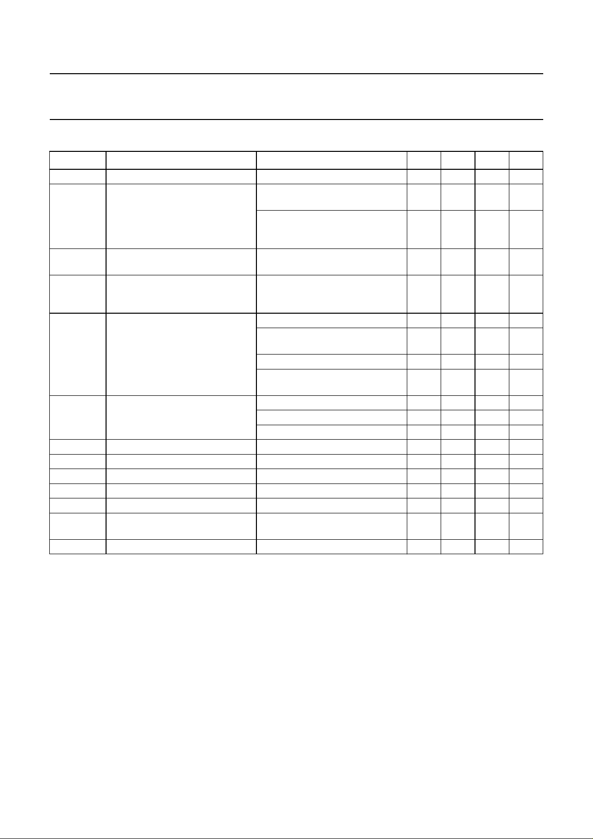
BLOCK DIAGRAM
handbook, full pagewidth
RSTOUT
DELAY
22 nF
INT
ALE
AD0
AD1
AD2
AD3
RD
WR
D0
D1
D2
D3
D4
D5
D6
D7
CS
I/OAUX
INTAUX
V
DD
100 nF
1
48
40
39
45
44
43
42
36
37
28
29
30
31
32
33
34
35
38
2
41
SUPPLY
AND
SUPERVISOR
ISO7816
UART
TIME-OUT
COUNTER
INTERFACE CONTROL
CLOCK
CIRCUIT
GND
V
DDA
220 nF
SAP SAM
STEP-UP
CONVERTER
ANALOG
DRIVERS
SEQUENCERS
AND
220 nF
SBP SBM
AGND
2524222621231927
20
6
4
8
10
9
3
5
7
14
12
16
18
17
11
13
15
V
UP
220 nF
C41
C81
CLK1
RST1
V
CC1
I/O1
PRES1
GNDC1
C42
C82
CLK2
RST2
V
CC2
I/O2
PRES2
GNDC2
TDA8007B
XTAL1 XTAL2
Fig.1 Block diagram.
2000 Nov 09 4
INT OSC
XTAL OSC
47 46
FCE534
Page 5

Philips Semiconductors Product specification
Double multiprotocol IC card interface TDA8007B
PINNING
SYMBOL PIN DESCRIPTION
RSTOUT 1 open-drain output for resetting external chips
I/OAUX 2 input or output for an I/O line issued of an auxiliary smart card interface
I/O1 3 data line to/from card 1 (ISO C7 contact)
C81 4 auxiliary I/O for ISOC8 contact (synchronous cards for instance) for card 1
PRES1 5 card 1 presence contact input (active HIGH or LOW by mask option)
C41 6 auxiliary I/O for ISOC4 contact (synchronous cards for instance) for card 1
GNDC1 7 ground for card 1
CLK1 8 clock output to card 1 (ISO C3 contact)
V
CC1
RST1 10 card 1 reset output (ISO C2 contact)
I/O2 11 data line to/from card 2 (ISO C7 contact)
C82 12 auxiliary I/O for ISO C8 contact (synchronous cards for instance) for card 2
PRES2 13 card 2 presence contact input (active HIGH or LOW by mask option)
C42 14 auxiliary I/O for ISO C4 contact (synchronous cards for instance) for card 2
GNDC2 15 ground for card 2
CLK2 16 clock output to card 2 (ISO C3 contact)
V
CC2
RST2 18 card 2 reset output (ISO C2 contact)
GND 19 ground connection
V
UP
SAP 21 contact 1 for the step-up converter (connect a low ESR 220 nF capacitor between pins SAP
SBP 22 contact 3 for the step-up converter (connect a low ESR 220 nF capacitor between pins SBP
V
DDA
SBM 24 contact 4 for the step-up converter (connect a low ESR 220 nF capacitor between pins SBP
AGND 25 ground connection for the step-up converter
SAM 26 contact 2 for the step-up converter (connect a low ESR 220 nF capacitor between pins SAP
V
DD
D0 28 data 0 or add 0
D1 29 data 1 or add 1
D2 30 data 2 or add 2
D3 31 data 3 or add 3
D4 32 data 4 or add 4
D5 33 data 5 or add 5
D6 34 data 6 or add 6
D7 35 data 7 or add 7
RD 36 read selection signal (read or write in non-multiplexed configuration)
9 card 1 supply output voltage (ISO C1 contact)
17 card 2 supply output voltage (ISO C1 contact)
20 output of the step-up converter
and SAM)
and SBM)
23 positive analog supply voltage for the step-up converter
and SBM)
and SAM)
27 positive supply voltage
2000 Nov 09 5
Page 6
Philips Semiconductors Product specification
Double multiprotocol IC card interface TDA8007B
SYMBOL PIN DESCRIPTION
WR 37 write selection signal (enable in case of non-multiplexed configuration)
CS 38 chip select input (active HIGH or LOW)
ALE 39 address latch enable in case of multiplexed configuration (connect toV
configuration)
INT 40 interrupt output (active LOW)
INTAUX 41 auxiliary interrupt input
AD3 42 register selection address 3
AD2 43 register selection address 2
AD1 44 register selection address 1
AD0 45 register selection address 0
XTAL2 46 connection pin for an external crystal
XTAL1 47 connection pin for an external crystal or input for an external clock signal
DELAY 48 connection pin for an external delay capacitor
in non-multiplexed
DD
handbook, full pagewidth
RSTOUT
I/OAUX
I/O1
C81
PRES1
C41
GNDC1
CLK1
V
CC1
RST1
I/O2
C82
DELAY
XTAL1
XTAL2
AD0
AD1
AD2
AD3
INTAUX
INT
ALE
CS
WR
48
47
46
45
44
43
42
41
40
39
38
37
1
2
3
4
5
6
7
8
9
10
11
12
13
14
15
C42
PRES2
GNDC2
TDA8007BHL
16
17
CC2
CLK2
V
18
RST2
19
GND
20
21
22
23
UP
SAP
V
SBP
DDA
V
24
SBM
36
35
34
33
32
31
30
29
28
27
26
25
FCE678
RD
D7
D6
D5
D4
D3
D2
D1
D0
V
DD
SAM
AGND
Fig.2 Pin configuration.
2000 Nov 09 6
Page 7
Philips Semiconductors Product specification
Double multiprotocol IC card interface TDA8007B
FUNCTIONAL DESCRIPTION
Throughoutthis specification, it isassumedthat the reader
is aware of ISO 7816 norm terminology.
Interface control
The TDA8007B can be controlled via an 8-bit parallel bus
(bits D0 to D7).
If a microcontroller with a multiplexed address/data bus
(suchasthe80C51) is used, then D0 to D7 may bedirectly
connected to P0 to P7. When CS is LOW, the
demultiplexing of address and data is performed internally
using the ALE signal, a LOW pulse on pin RD allows the
selected register to be read, a LOW pulse on pin WR
allows the selected register to be written to. The
TDA8007B automatically switches to the multiplexed bus
configurationif a rising edgeis detected on pin ALE.In this
event, AD0 to AD3 play no role and may be tied to VDDor
GND. Using a 80C51 microcontroller, the TDA8007B is
simply controlled with MOVX instructions.
If ALE is tied to VDDor GND, then the TDA8007B will be in
the non-multiplexed configuration. In this case, the
address bits are external pins AD0 to AD3, RD is the
read/write control signal, and WR is a data write or read
active LOW enable signal.
In both configurations, the TDA8007B is selected only
when CS is LOW. INT is an active LOW interrupt signal.
In non-multiplexed bus configuration, CS and EN play the
same role.
In read operations (RD/WR is HIGH), the data
corresponding to the chosen address is available on the
bus when both CS and EN are LOW.
In write operations, the data present on the bus is written
when signals RD/WR, CS and EN become LOW.
handbook, full pagewidth
AD0 to AD3
CS
D0 to D7
ALE
WR
RD
LATCH
REC
MUX
MUX
RD
WR
addresses
REGISTERS
Fig.3 Multiplexed bus recognition.
FCE679
2000 Nov 09 7
Page 8
Philips Semiconductors Product specification
Double multiprotocol IC card interface TDA8007B
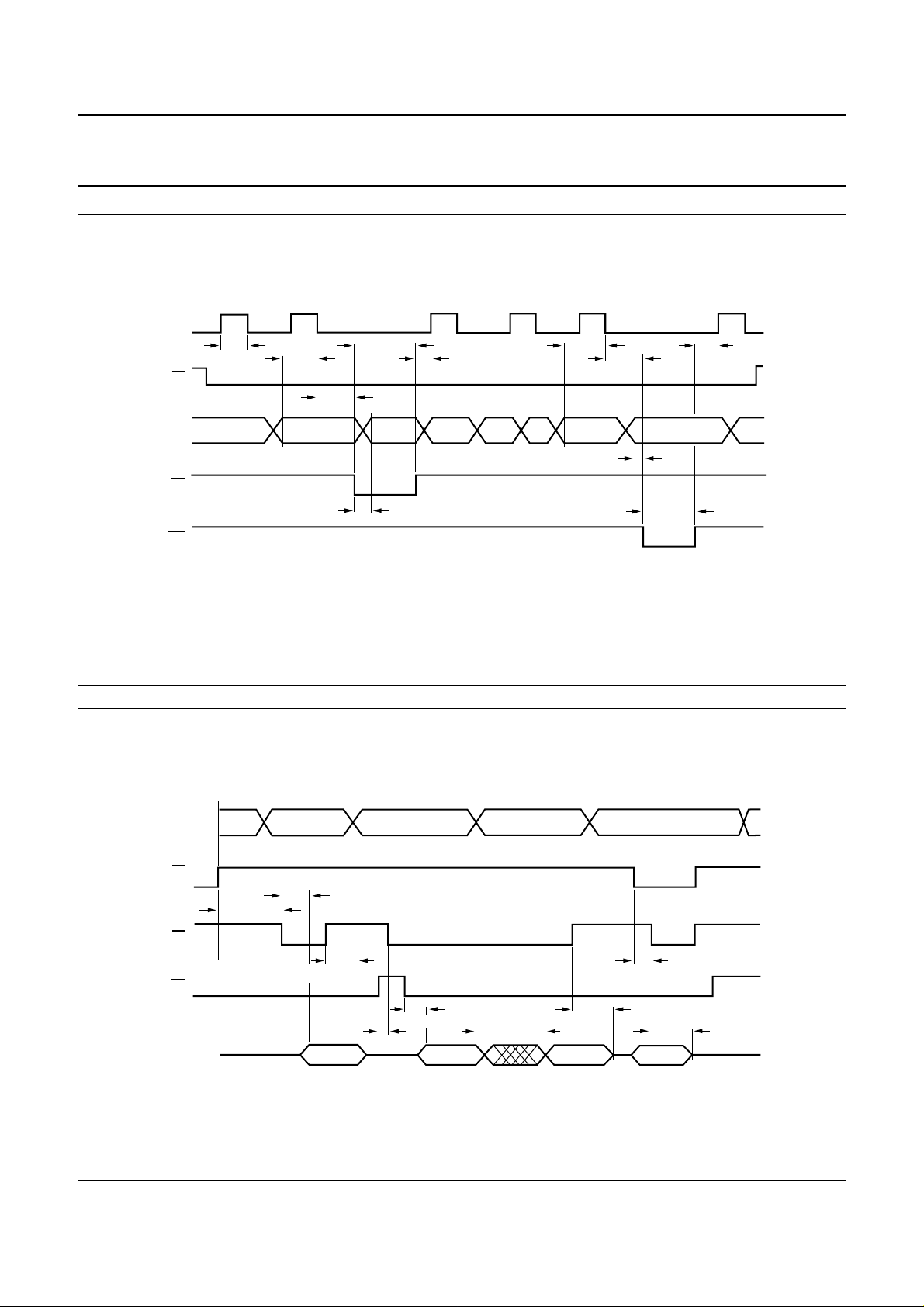
handbook, full pagewidth
ALE
CS
D0 to D7
RD
WR
t
W(ALE)
t
AVLL
t
(AL-RWL)
ADDRESS
t
W(RD)
DATA
READ
t
(RL-DV)
t
(RWH-AH)
Fig.4 Control with multiplexed bus.
t
AVLL
t
(AL-RWL)
ADDRESS
t
(DV-WL)
t
(RWH-AH)
DATA WRITE
t
W(WR)
FCE680
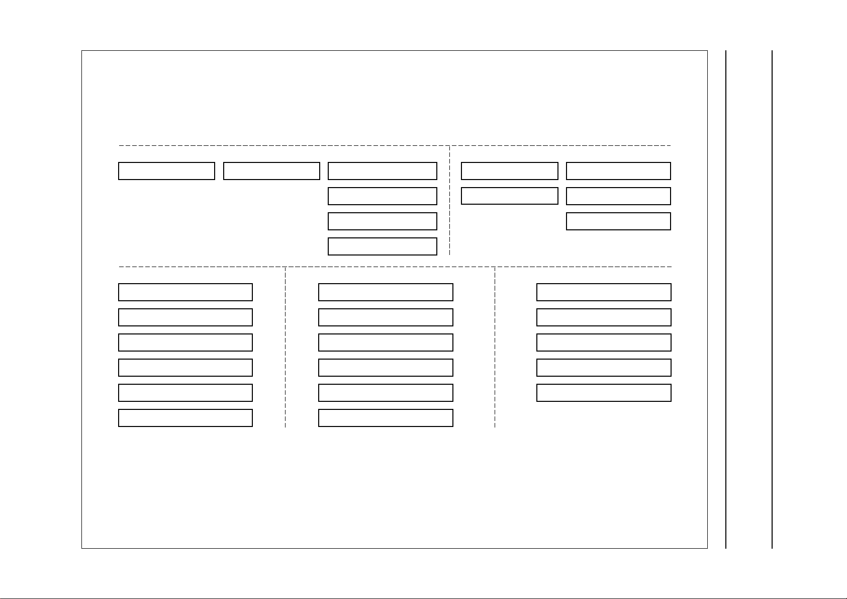
handbook, full pagewidth
AD0 to AD3
RD
CS
EN
D0 to D7
t
(REH-CL)
Read Read Read
t
(CEL-DV)
t
(CEH-DZ)
t
(CEL-DV)
t
DATA OUT
(REH-CL)
DATA OUT DATA OUT DATA IN
Fig.5 Control with non-multiplexed bus.
2000 Nov 09 8
t
(AD-DV)
t
(CEH-DZ)
Write (data written on
falling edge of CS)
t
(RL-CEL)
t
(CREL-DZ)
FCE681
Page 9

Philips Semiconductors Product specification
Double multiprotocol IC card interface TDA8007B
Control registers
The TDA8007B has 2 complete analog interfaces which
can drive card 1 and card 2. The data to and from these
2 cards share the same ISO UART. The data to and from
athirdcard (card 3), externally interfaced(withaTDA8002
or TDA8003 for example), may also share the same
ISO UART.
Cards 1, 2 and 3 have dedicated registers for setting the
parameters of the ISO UART; Programmable Divider
Register (PDR), Guard Time Register (GTR), UART
Configuration Register 1 (UCR1), UART Configuration
Register 2 (UCR2) and Clock Configuration Register
(CCR).
Cards 1and 2 also have dedicated registersfor controlling
their power and clock configuration. The Power Control
Register (PCR) for card 3, is controlled externally. The
PCR is also used for writing or reading on the auxiliary
card contacts C4 and C8.
Card 1,2 or 3canbeselectedvia the Card Select Register
(CSR). When one card is selected, the corresponding
parameters are used by the ISO UART. The CSR also
contains one bit for resetting the ISO UART (active LOW).
This bit is reset after Power-on, and must be set to HIGH
before starting with any one of the cards. It may be reset
by software when necessary.
The Hardware Status Register (HSR) gives the status of
the supply voltage, of the hardware protections and of the
card movements.
HSR and USR give interrupts on pin INT when some of
their bits have been changed.
The MSR does not give interrupts and may be used in the
pollingmode for some operations;for this use, someof the
interrupt sources within the USR and HSR may be
masked.
A 24-bit time-out counter may be started to give an
interrupt after a number of ETUs programmed into
registers TOR1, TOR2 and TOR3. This will help the
microcontroller in processing different real-time tasks
(ATR, WWT, BWT, etc.) mainly if the microcontrollers and
cards clock are asynchronous.
Thiscounterisconfigured with a register Time-Out counter
Configuration (TOC). It may be used as a 24-bit or as a
16 + 8 bits. Each countercan be setto start counting once
data has been written, or on detection of a start bit on the
I/O, or as auto-reload.
When the specific parameters of the cards have been
programmed, the UART may be used with the following
registers: UART Receive Register (URR), UART Transmit
Register (UTR), UART Status Register (USR) and Mixed
StatusRegister(MSR).Inreceptionmode, a FIFO of 1 to 8
characters may be used, and is configured with the FIFO
Control Register (FCR).
2000 Nov 09 9
Page 10
This text is here in white to force landscape pages to be rotated correctly when browsing through the pdf in the Acrobat reader.This text is here in
_white to force landscape pages to be rotated correctly when browsing through the pdf in the Acrobat reader.This text is here inThis text is here in
white to force landscape pages to be rotated correctly when browsing through the pdf in the Acrobat reader. white to force landscape pages to be ...
2000 Nov 09 10
Philips Semiconductors Product specification
Double multiprotocol IC card interface TDA8007B
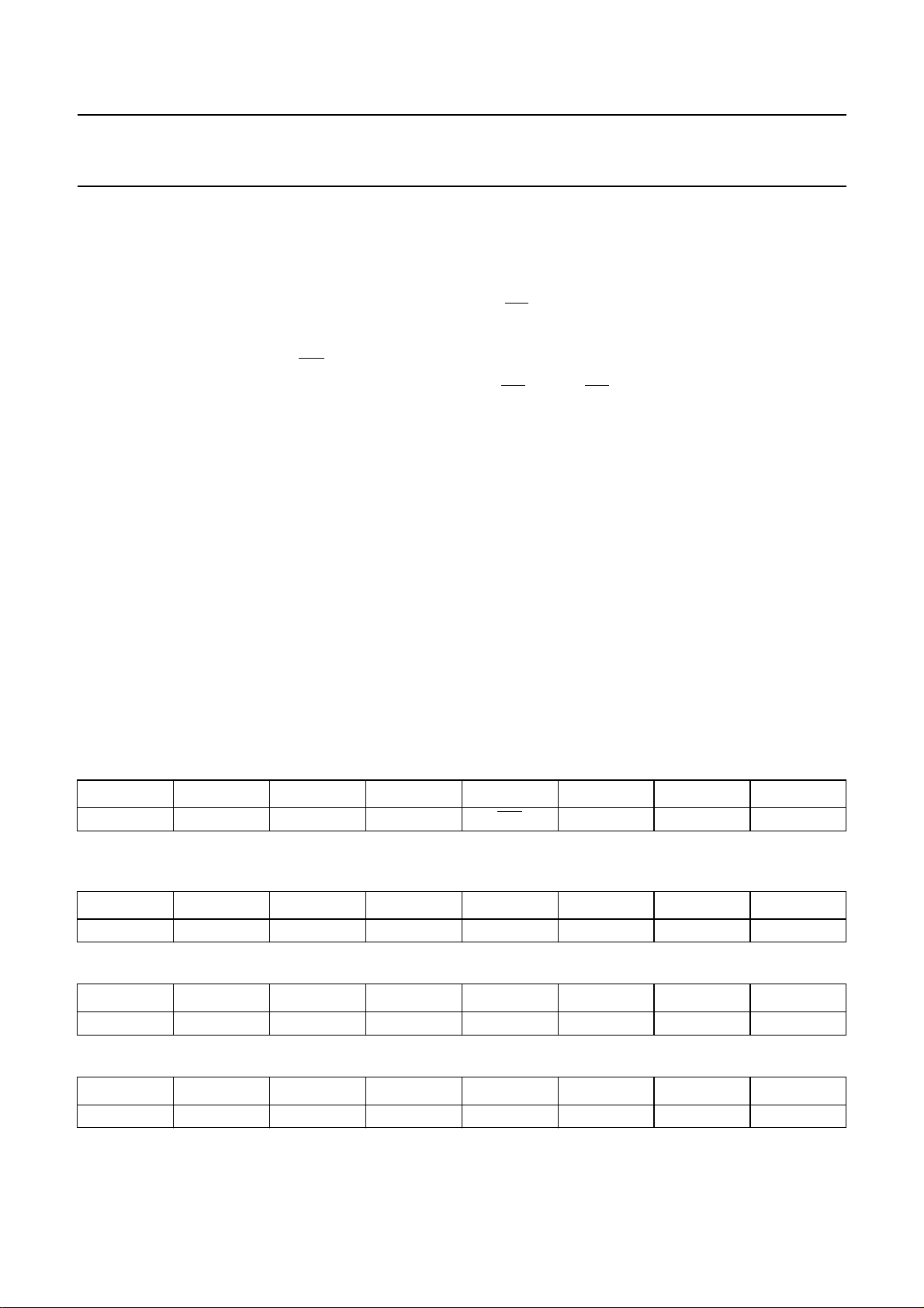
GENERAL
CARD SELECT REGISTER HARD STATUS REGISTER
CARD1
PROGRAM DIVIDER REGISTER 1
GUARD TIME REGISTER 1
UART CONFIGURATION REGISTER 11
UART CONFIGURATION REGISTER 12
CLOCK CONFIGURATION REGISTER 1
POWER CONTROL REGISTER 1
TIME-OUT REGISTER 1
TIME-OUT REGISTER 2
TIME-OUT REGISTER 3
TIME-OUT CONFIGURATION
CARD2
PROGRAM DIVIDER REGISTER 2
GUARD TIME REGISTER 2
UART CONFIGURATION REGISTER 21
UART CONFIGURATION REGISTER 22
CLOCK CONFIGURATION REGISTER 2
POWER CONTROL REGISTER 2
ISO UART
UART STATUS REGISTER
MIXED STATUS REGISTER
UART CONFIGURATION REGISTER 31
UART CONFIGURATION REGISTER 32
CLOCK CONFIGURATION REGISTER 3
UART TRANSMIT REGISTER
UART RECEIVE REGISTER
FIFO CONTROL REGISTER
CARD3
PROGRAM DIVIDER REGISTER 3
GUARD TIME REGISTER 3
FCE682
Fig.6 Registers summary.
handbook, full pagewidth
Page 11
Philips Semiconductors Product specification
Double multiprotocol IC card interface TDA8007B
GENERAL REGISTERS
The Card Select Register (see Table 1) is used for
selecting the card on which the UART will act, and also to
reset the ISO UART.
If SC1 = 1, then card 1 is selected; if SC2 = 1, then card 2
is selected, if SC3 = 1, then card 3 is selected. These bits
must be set oneat a time.After reset, card 1is selected by
default. The bit Reset ISO UART (RIU) must be set to
logic 1 by software before any action on the UART can
take place. When reset, this bit resets all UART registers
to their initial value.
It should be noted that access to card 3 is only possible
once either card 1 or 2 has been activated.
The Hardware Status Register (see Table 2) gives the
status of the chip after a hardware problem has been
detected.
Presence Latch 1 (PRL1) and Presence Latch 2 (PRL2)
are HIGH when a change has occurred on PR1 and PR2.
SupervisorLatch(SUPL) is HIGH when thesupervisorhas
been activated.
Protection 1 (PRTL1) and Protection 2 (PRTL2) are HIGH
when a default has been detected on card readers 1
and 2. (PRTL is the OR function of protection on VCCand
RST).
PTL is set if overheating has occurred.
INTAUXL is HIGH if the level on the INTAUX input has
been changed.
When PRTL2, PRTL1, PRL2 or PRL1 or PTL is HIGH,
then INT is LOW. The bits having caused the interrupt are
cleared when the HSR has been read-out. The same
occurs with bit INTAUXL if not disabled.
Atpower-on, or after asupplyvoltage dropout, SUPL is set
and INT is LOW. INT will return HIGH at the end of the
alarm pulse on pin RSTOUT. SUPL will be reset only after
a status register read-out outside the ALARM pulse
(see Fig.7).
In case of emergency deactivation (by PRTL1, PRTL2,
SUPL, PRL2, PRL1 or PTL), the START bit is
automatically reset by hardware.
The three registers TOR1, TOR2 and TOR3 form a
programmable 24-bit ETU counter, or two independant
counters (one 16-bit and one 8-bit).
The value to load in TOR1, 2 and 3 isthe number of ETUs
to count.
The TOC register is used for setting different
configurations of the time-out counter as given in Table 7
(all other configurations are undefined).
Table 1 Card select register (write and read); address: 0
(all significant bits are cleared after reset, except for SC1 which is set)
CS7 CS6 CS5 CS4 CS3 CS2 CS1 CS0
not used not used not used not used
Table 2 Hardware status register (read only); address: F
(all significant bits are cleared after reset, except for SUPL which is set within the RSTOUT pulse)
HS7 HS6 HS5 HS4 HS3 HS2 HS1 HS0
not used PRTL2 PRTL1 SUPL PRL2 PRL1 INTAUXL PTL
Table 3 Time-out register 1 (write only); address: 9 (all bits are cleared after reset)
TO17 TO16 TO15 TO14 TO13 TO12 TO11 TO10
TOL7 TOL6 TOL5 TOL4 TOL3 TOL2 TOL1 TOL0
Table 4 Time-out register 2 (write only); address: A (all bits are cleared after reset)
TO27 TO26 TO25 TO24 TO23 TO22 TO21 TO20
TOL15 TOL14 TOL13 TOL12 TOL11 TOL10 TOL9 TOL8
RIU SC3 SC2 SC1
2000 Nov 09 11
Page 12

Philips Semiconductors Product specification
Double multiprotocol IC card interface TDA8007B
Table 5 Time-out register 3 (write only); address: B (all bits are cleared after reset)
TO37 TO36 TO35 TO34 TO33 TO32 TO31 TO30
TOL23 TOL22 TOL21 TOL20 TOL19 TOL18 TOL17 TOL16
Table 6 Time-out configuration register (read and write); address: 8 (all bits are cleared after reset)
TOC7 TOC6 TOC5 TOC4 TOC3 TOC2 TOC1 TOC0
TOC7 TOC6 TOC5 TOC4 TOC3 TOC2 TOC1 TOC0
Table 7 Time-out counter configurations
TOC OPERATING MODE
00 all counters are stopped
61 Counter 1 is stopped, and counters 3 and 2 form a 16-bit counter. Counting the value stored in TOR3
and TOR2 is started after 61 is written in the TOC. An interrupt is given, and bit TO3 is set within the
USR when the terminal count is reached. The counter is stopped by writing 00 in the TOC.
65 Counter 1 is an 8-bit auto reload counter, and counters 3 and 2 form a 16-bit counter. Counter 1 starts
counting the content of TOR1on the first start bit (reception or transmission) detected on I/O after 65 is
written in the TOC.When counter 1 reaches its terminal count, an interrupt is given, bit TO1in the USR
is set, and the counter automatically restarts the same count until it is stopped. It is not allowed to
change the content of TOR1 during a count. In this mode, the accuracy of counter 1 is ±0.5 ETU.
Counters 3 and 2 are wired as a single 16-bit counter and starts counting the value TOR3 and TOR2
when 65 is written in the TOC. When the counter reaches its terminal count, an interrupt is given and
bit TO3 is set within the USR. Both counters are stopped when 00 is written in the TOC.
68 Counters 3, 2 and 1 are wired as a single 24-bit counter. Counting the value stored in TOR3, TOR2 and
TOR1 is started after 68 is written in the TOC. The counter is stopped by writing 00 in the TOC. It is not
allowed to change the content of TOR3, TOR2 and TOR1 within a count.
7C Counters 3, 2 and 1 are wired as a single 24-bit counter. Counting the valuestored in TOR3, TOR2 and
TOR1 on the first start bit detected on I/O (reception or transmission) after the value has been written.
It is possible to change the content of TOR3, TOR2and TOR1during a count; the current count will not
be affected and the new count value will be taken into account at the next start bit. The counter is
stopped by writing 00 in the TOC. In this configuration TOR3, TOR2 and TOR1 must not be all zero.
E5 Same configuration as TOC = 65, except that counter 1 will be stopped at the end of the 12th ETU
following the first start bit detected after E5 has been written in the TOC.
2000 Nov 09 12
Page 13

Philips Semiconductors Product specification
Double multiprotocol IC card interface TDA8007B
Thetime-outcounterisveryuseful for processing the clock
counting during ATR, the Work Waiting Time, or the
waiting times defined in T = 1 protocol. It should be noted
that the 200 and 400 CLK counter used during ATR is
done by hardware when the start session is set; a specific
hardware controls functionality BGT in T = 1 protocol, and
a specific register is available for processing the extra
guard time.
The possible use of the counters is as follows:
• ATR (cold reset):
– Before activation; TOR1 = C0H, TOR2 = 6EH,
TOR3 = 0andTOC = 65. Once activated, timer 2 + 3
will count 40920 clock pulses before giving an
interrupt.
– On interrupt; TOR2 = 76H and TOC = 65. If a
character is received from the card before the
timeout,thencounter 1willbeenabled.Counter 1will
give one interrupt every 192 ETUs, so the software
will count 100 times to verify that the ATR is finished
before 19200 ETUs. The UART will give an interrupt
with bit Buffer Full (BF) at 10.5 ETUs after the start
bit.
– On interrupt; TOR3 = 25H, TOR2 = 80H and
TOC = 65. Counter 1 keeps on counting
100 × 192 ETUs, while counter 2 and 3 counts
9600 ETUs. This sequence is repeated until the
character before the last one of the ATR.
– On interrupt TOR3 = 25H, TOR2 = 80H and
TOC = E5. Timer 1 will be automatically stopped at
the end of the last character of the ATR, allowing a
count of 19200 ETUs.
– On interrupt TOC = 00.
• Work Waiting Time (WWT) in T = 0 protocol;
– Before sending the first command to the card
TOR1, TOR2 and TOR3 should be loaded with the
correct 960 × WI × D value and TOC = 7C
– Timer 3, 2 and 1 will count the WWT between each
start bit
• Character Waiting Time (CWT) and Block Waiting Time
(BWT) in T = 1 protocol:
– Before sending the first block to the card, TOR3,
TOR2and TOR1 should be loaded withtheCWT and
TOC=7C
– Timer 3 + 2 + 1 will count the CWT between each
start bit
– Before the end of the block, TOR3, TOR2 and TOR1
should be loaded with the BWT
– Timer3+2+1willcount the BWT from the last start
bit of the sent block
– After reception of the first character of the block from
the card, TOR3, TOR2 and TOR1 should be loaded
with the CWT
– Timer3+2+1 will count the CWT between each
received start bit
– And so on.
• Before and after CLOCK STOP (example, where
ETU = 372 clock pulses):
– After the last received character on I/O, TOR3 = 0,
TOR2 = 6 and TOC = 61
– Timer3+2 will start counting 2232 clock pulses
before giving an interrupt
– On interrupt, the software may stop the clock to the
card
– When it is necessary to restart the clock, TOR3 = 0,
TOR2 = 2, TOC = 61 and restart the clock
– Timer3+2 gives an interrupt at 744 clock pulses,
and then the software can send the first command to
the card.
ISO UARTREGISTERS
When the microcontroller wants to transmit a character to
the selected card, it writes the data in direct convention in
the UART Transmit Register (see Table 8). The
transmission:
• Starts at the end of writing (on the rising edge of WR) if
the previous character has been transmitted and if the
extra guard time has expired; or
• Starts at the end of the extra guard time if this one has
not expired; or
• Does not start if the transmission of the previous
character is not completed.
In the case of a synchronous card (bit SAN within UCR2
is set), only D0 is relevant, and is copied on the I/O of the
selected card. When the microcontroller wants to read
data from the card it reads it from the UART Receive
Register (see Table 9) in direct convention.
In case ofa synchronous card, only D0 isrelevant and is a
copy of the state of the selected card I/O.
When needed, this register may be tied to a FIFO whose
length ‘n’ is programmable between 1 and 8.
If n > 1, then no interrupt is given until the FIFO is full. The
microcontroller may empty the FIFO at any time.
2000 Nov 09 13
Page 14

Philips Semiconductors Product specification
Double multiprotocol IC card interface TDA8007B
Error management in protocol:
• T=0:
In the event of a parity error, the received byte is not
stored in the FIFO, and the error counter is incremented.
The error counter is programmable between 1 and 8.
When the programmed number is reached, bit PE is set
in the status register USR and INT goes LOW. The error
counter must be reprogrammed to the desired value after
its count has been reached.
• T=1:
In the event of a parity error, the character is loaded in the
FIFO, and bit PE is set whatever the programmed value
in parity error counter.
When the FIFO is full, bit RBF in the status register USR
is set. This bit is reset when at least one character has
been read from the URR.
When the FIFO is empty, bit FE is set as long as no
character has been received.
The Mixed Status Register (see Table 10) relates the
status of pin INTAUX, the cards presence contacts PR1
and PR2, the BGT counter, the FIFO empty indication
and the transmit/receive ready indicator TBE/RBF.
Bit INTAUX is set when the level on pin INTAUX is HIGH,
it is reset when the level is LOW.
Bit BGT is linked with a 22 ETU counter, which is started
at every start bit on the I/O. Bit BGT is set if the count is
finished before the next start bit. This helps to verify that
the card has not answered before 22 ETUs after the last
transmitted character, or not transmitting a character
before 22 ETUs after the last received character.
PR1 is HIGH when card 1 is present, PR2 is HIGH when
card 2 is present.
FE is set when the reception FIFO is empty. It is reset
when at least one character has been loaded in the FIFO.
Bit TBE/RBF(Transmit Buffer Empty/Receive BufferFull)
is set when:
• Changing from reception mode to transmission mode
• A character has been transmitted by the UART
• The reception FIFO is full.
Bit TBE/RBF is reset after Power-on or after one of the
following:
• When bit RIU is reset
• When a character has been written to the UTR
• When at least one character has been read in the FIFO
• When changing from transmission mode to reception
mode.
No bits within the MSR act upon INT:
• The FIFO Control Register bits are given in Table 11,
FL2, FL1 and FL0 determine the depth of the FIFO
(000 = length 1, 111 = length 8).
PEC2, PEC1 and PEC0 determine the number of parity
errors before setting bit PE in the USR and pulling
INT LOW; 000 indicates that if only one parity error has
occurred,bit PEisset;111 indicates that bit PE will be set
after 8 parity errors.
PEC2, PEC1 and PEC0 need to be reprogrammed to the
desired value after bit PE has been set.
In protocol T = 0:
• If a correct character is received before the
programmed error numberis reached the error counter
will be reset.
• If the programmed number of allowed parity errors is
reached, bit PE in the USR will be set as long as the
USR has not been read.
In protocol T = 1:
• The error counter has no action (bitPE is set at the first
wrong received character).
• The UART Status Register (see Table 12) is used by
the microcontroller to monitor the activity of the
ISO UART and that of the time-out counter.
Transmission Buffer Empty (TBE) is HIGH when the
UART is in transmission mode, and when the
microcontroller may write the next characterto transmit in
the UTR. It is reset when the microcontroller has written
data in the transmit register or when bit T/R within UCR1
has been reset either automatically or by software.
After detection of a parity error in transmission, it is
necessary to wait 13 ETUs before rewriting the character
which has been Not ACKnowledged (NAK) by the card.
ReceptionBufferFull (RBF) is HIGH when the FIFOisfull.
The microcontroller may read some of the characters in
the URR, which clears bit RBF.
TBE and RBFsharethe same bit within the USR (when in
transmission mode, the relevant bit is TBE; when in
reception mode, it is RBF).
Framing Error (FER) is HIGH when the I/O was not in the
high-impedance state at 10.25 ETUs after a start bit. It is
reset when the USR has been read-out.
2000 Nov 09 14
Page 15

Philips Semiconductors Product specification
Double multiprotocol IC card interface TDA8007B
Overrun (OVR) is HIGH if the UART has received a new
characterwhilst the FIFO wasfull.In this case, atleast one
character has been lost.
InprotocolT = 0:Parity Error (PE) is HIGH iftheUARThas
detected a number of received characters with parity
errors equal to the number written in PEC2, PEC1 and
PEC0 or if a transmitted characterhas been NAKedby the
card.
In protocol T = 0:a character received with a parity error is
not stored in the FIFO (the card is supposed to repeat this
character).
In protocol T = 1:a character with a parity error is storedin
the FIFO and the parity error counter is not active.
Early Answer (EA) is HIGH if the first start bit on the I/O
during ATR hasbeen detected between 200 and 384 CLK
Table 8 UART transmit register (write only); address: D (all bits are cleared after reset)
UT7 UT6 UT5 UT4 UT3 UT2 UT1 UT0
UT7 UT6 UT5 UT4 UT3 UT2 UT1 UT0
Table 9 UART receive register (read only); address: D (all bits are cleared after reset)
pulses (all activities on the I/O during the 200 first CLK
pulseswithRST LOWorHIGHare not taken into account).
These 2 features are reinitialized at each toggling of RST.
Bit TO1 is set when counter 1 has reached its terminal
count.
Bit TO3 is set when counter 3 has reached its terminal
count.
If any of the status bits FER, OVR, PE, EA, TO1 or TO3
are set then INT will go LOW. The bit having caused the
interrupt is reset at the endof a readoperation of the USR.
If TBE/RBF is set, and if the mask bit DISTBE/RBF within
USR2 is not set, then INT will also be LOW. TBE/RBF is
reset when data has been written to the UTR, when data
has been read from the URR, or when changing from
transmission mode to reception mode.
UR7 UR6 UR5 UR4 UR3 UR2 UR1 UR0
UR7 UR6 UR5 UR4 UR3 UR2 UR1 UR0
Table 10 Mixed status register (read only); address: C
(bits TBE, RBF and BGT are cleared after reset; bit FE is set after reset)
MS7 MS6 MS5 MS4 MS3 MS2 MS1 MS0
not used FE BGT not used PR2 PR1 INTAUX TBE/RBF
Table 11 FIFO control register (write only); address: C (all relevant bits are cleared after reset)
FC7 FC6 FC5 FC4 FC3 FC2 FC1 FC0
not used PEC2 PEC1 PEC0 not used FL2 FL1 FL0
Table 12 UART status register (read only); address: E (all bits are cleared after reset)
US7 US6 US5 US4 US3 US2 US1 US0
TO3 not used TO1 EA PE OVR FER TBE/RBF
2000 Nov 09 15
Page 16

Philips Semiconductors Product specification
Double multiprotocol IC card interface TDA8007B
CARD REGISTERS
When cards 1 2 or 3 are selected, then the following registers may be used for programming some specific parameters.
The Programmable Divider Register (see Table 13) is used for counting the cards clock cycles forming the ETU. It is an
auto-reload 8-bit counter decounting from the programmed value down to 0.
Table 13 Programmable Divider Register (PDR1, 2 and 3) (read and write); address: 2 (all bits are cleared after reset)
PD7 PD6 PD5 PD4 PD3 PD2 PD1 PD0
PD7 PD6 PD5 PD4 PD3 PD2 PD1 PD0
The UART Configuration Register 2 bits are given in Table 14. If bit PSC is set to logic 1, then the prescaler value is 32.
If bit PSC is set to logic 0, then the prescaler value is 31. One ETU will last a number of card clock cycles equal to
prescaler x PDR. All baud rates specified in ISO 7816 norm are achievable with this configuration.
Table 14 UART configuration register 2 (UCR21, 22 and 23) (read and write); address: 3
(all relevant bits are cleared after reset)
UC27 UC26 UC25 UC24 UC23 UC22 UC21 UC20
not used DISTBE/RBF DISAUX PDWN SAN
Table 15 Baud rates with a 3.58 MHz card clock frequency (31;12 means prescaler set to 31 and PDR set to 12)
D
1 31;12
2 31;6
3 31;3
4 31;3
5 31;3
6 32;1 32;2
8 31;1
9 31;3
0123456910111213
9600
19200
38400
115200
31;12
9600
31;6
19200
31;3
38400
31;1
115200
31;18
6400
31;9
12800
31;24
4800
31;12
9600
31;6
19200
38400
31;2
57600
31;36
3200
31;18
6400
31;9
12800
31;3
38400
31;48
2400
31;24
4800
31;12
9600
31;6
19200
38400
31;4
28800
F
31;60
1920
31;30
3840
31;15
7680
31;5
23040
38400
AUTOCONV CKU PSC
32;16 32;24 32;32 32;48 32;64
32;8 32;12 32;16 32;24 32;32
32;4 32;6 32;8 32;12 32;16
32;2 32;3 32;4 32;6 32;8
32;1 32;2 32;3 32;4
32;2 32;4
2000 Nov 09 16
Page 17

Philips Semiconductors Product specification
Double multiprotocol IC card interface TDA8007B
For other baud rates than those given in Table 15, there
is the possibility to set bit CKU (clock UART)to logic 1. In
this case, the ETU will last half of the formula given
above.
If bit AUTOCONV is set, then the convention is set by
software using bit CONV in the UART Configuration
Register. If it is reset, then the configuration is
automatically detected on the first received character
whilst the Start Session (SS) bit is set.
Synchronous/Asynchronous (SAN) is set by software if a
synchronous card is expected. The UART is then
bypassed, and only bit 0 in the URR and UTR is
connected to the I/O.In this case the CLK is controlledby
bit SC in the CCR.
When Power-down mode (PDWN) is set by software, the
crystal oscillator is stopped. This mode allows low
consumption in applications where it is required. During
this mode, it is not possible to select another card other
than the currently selected one. There are 5 ways of
escaping from the Power-down mode:
1. Insert card 1 or card 2
2. Withdraw card 1 or card 2
3. Select the TDA8007B by resetting CS (this assumes
that the TDA8007Bhad been deselectedafter setting
Power-down mode)
4. INTAUXL has been set due to a change on pin
INTAUX
5. If CS is permanently set to LOW, reset bit PDWN by
software.
After any of these 5 events, the TDA8007B will leave the
Power-downmode,andwillpull INT LOW when it is ready
to communicate with the system microcontroller. The
system microcontroller may then read the status
registers, and INT will return HIGH (if the system
microcontroller has woken the TDA8007B by reselecting
it, then no bits will be set in the status registers).
If the Disable AUX (DISAUX) interrupt bit in UCR2 is set,
then a change on INTAUX will not generate an interrupt
(but bit INTAUXL in the HSR will be set; it is therefore
necessary to read the HSR before a DISAUX reset to
avoid an interrupt by INTAUXL). To avoid an interrupt
during a change of card, it is better to set the DISAUX bit
in UCR2 for both cards.
If the DisableTBE/RBF (DISTBE/RBF) interrupt bit is set,
then reception or transmission of a character will not
generate an interrupt:
• This feature is useful for increasing communication
speed with the card; in this case, a copy of the
TBE/RBF bit within the MSR must be polled (and not
the original) in order not to loose priority interrupts
which can occur in the USR.
• The Guard Time Register (see Table 17) is used for
storing the number of guard ETUs given by the card
during ATR. In transmission mode, the UART will wait
this number of ETUs before transmitting the character
stored in the UTR. In T = 1 protocol, when GTR = FF
means operation at 11 ETUs. In protocol T = 0,
GTR = FF means operation at 12 ETUs.
• The UART Configuration Register (see Table 18) is
used for setting the parameters of the ISO UART.
The Convention (CONV) bit is set if the convention is
direct. CONV is either automatically written by hardware
according to the convention detected during ATR, or by
software if the bit AUTOCONV is set.
The SS bit is set before ATR for automatic convention
detection and early answer detection (this bit must be
reset by software after reception of a correct initial
character).
The Last Character to Transmit (LCT) bit is set by
software before writing the last character to be
transmitted in the UTR. It allows automatic change to
reception mode. It is reset by hardware at the end of a
successful transmission.
The Transmit/Receive (T/R) bit is set by software for
transmission mode. A change from logic 0 to logic 1 will
set bit TBE in the USR. Bit T/R is automatically reset by
hardwareif the LCTbit has beenused before transmitting
the last character.
The Protocol (PROT) bit is set if the protocol type is
asynchronous T = 1. If PROT = 0, the protocol is T = 0.
The Flow Control (FC) bit is set if flow control is used (not
described in this specification).
If the Force Inverse Parity (FIP) bit is set to HIGH the
UART will NAK a correctly received character, and will
transmit characters with wrong parity bits.
2000 Nov 09 17
Page 18

Philips Semiconductors Product specification
Double multiprotocol IC card interface TDA8007B
Clock Configuration Register (see Table 19):
• For cards 1 and 2, the CCR defines the clock for the
selected card.
• For cards 1, 2 and 3 it defines the clock to the
ISO UART. It should be noted that if bit CKU in the
prescaler register of the selected card is set, then the
ISO UART is clocked at twice the frequency of the card,
which allows baud rates not foreseen in ISO 7816 norm
to be reached.
In case of an asynchronous card, theClock Stop (CST) bit
defines whether the clock to the card is stopped or not.
If CST is set, then CLK is stopped LOW if SHL = 0, and
HIGH if SHL = 1.
If CST is reset, then CLK is determined by bits AC0, AC1
and AC2; see Table 16. All frequency changes are
synchronous, thus ensuring that no spike or unwanted
pulse widths occur during changes.
Table 16 CLK value for an asynchronous card
AC2 AC1 AC0 CLK
000
001
010
011
100
101
110
111
When switching from XTAL/n to1⁄2f
int
1
⁄
XTAL
2
1
⁄
XTAL
2
1
⁄
XTAL
4
1
⁄
XTAL
8
1
⁄
f
2
int
1
⁄
f
2
int
1
⁄
f
2
int
1
⁄
f
2
int
or vice verse, only
bit AC2 must be changed (AC1 and AC0 must remain the
same). When switching from XTAL/n or1⁄2f
to CLK
int
STOP or vice verse, only bits CST and SHL must be
changed.
When switching from XTAL/n to1⁄2f
or vice verse, a
int
maximum delay of 200 µs can occur between the
commandand the effective frequency changeon CLK(the
fastest switching time is from1⁄2XTAL to1⁄2f
verse, the best for duty cycle is from1⁄8XTAL to1⁄2f
or vice
int
or
int
vice verse).
It is necessary to wait the maximum delay time before
reactivating from Power-down mode.
In the event of a synchronous card, then the CLK contact
isthe copy of the valuewrittenin Synchronous Clock (SC).
In reception mode, the data from the card is available to
UR0 after a read operation of the URR; in transmission
mode, the data is written on the I/O line of the card when
theUTRhasbeenwrittento and remains unchanged when
another card is selected.
The Power Control Register (PCR), see Table 20:
• Starts or stops card sessions.
• Reads or writes on auxiliary card contacts C4 and C8.
• Is available only for cards 1 or 2.
If the microcontroller sets START to logic 1, then the
selected card is activated (see Section “Activation
sequence”).If the microcontroller resets STARTto logic 0,
then the card is deactivated (see Section “Deactivation
sequence”). START is automatically reset in case of
emergency deactivation.
If 3 V/5 V is set to logic 1, then VCCis 3 V. If 3 V/5 V is set
to logic 0, then VCC is 5 V.
When the card is activated, RST is the copy of the value
written in RSTIN.
If 1.8 V is set, then VCC= 1.8 V: It should be noted that no
specification is guaranteed at this voltage.
When writing to the PCR, C4 will output the value written
to PCR4,and C8thevaluewrittento PCR5.Whenreading
fromthe PCR, PCR4 will storethevalue on C4, and PCR5
the value on C8.
Table 17 Guard time register (GTR1, 2 and 3) (read and write); address: 5 (all bits are cleared after reset)
GT7 GT6 GT5 GT4 GT3 GT2 GT1 GT0
GT7 GT6 GT5 GT4 GT3 GT2 GT1 GT0
Table 18 UART configuration register 1 (UCR11, 12 and 13) (read and write); address: 6
(all relevant bits are cleared after reset)
UC7 UC6 UC5 UC4 UC3 UC2 UC1 UC0
not used FIP FC PROT T/R LCT SS CONV
2000 Nov 09 18
Page 19

Philips Semiconductors Product specification
Double multiprotocol IC card interface TDA8007B
Table 19 Clock configuration register (CCR1, 2 and 3) (read and write); address: 1 (all bits are cleared after reset)
CC7 CC6 CC5 CC4 CC3 CC2 CC1 CC0
not used not used SHL CST SC AC2 AC1 AC0
Table 20 Power control register (PCR1and 2) (read and write); address: 7 (all relevant bits are cleared after reset)
PCR7 PCR6 PCR5 PCR4 PCR3 PCR2 PCR1 PCR0
not used not used C8 C4 1V8 RSTIN 3V/5V START
Table 21 Register summary
NAME ADDR R/W 7 6 543210
CSR 00 R/W not
used
HSR 0F R not
used
MSR 0C R not
used
TOR1 09 W TOL7 TOL6 TOL5 TOL4 TOL3 TOL2 TOL1 TOL0 00000000
TOR2 0A W TOL15 TOL14 TOL13 TOL12 TOL11 TOL10 TOL9 TOL8 00000000
TOR3 0B W TOL23 TOL22 TOL21 TOL20 TOL19 TOL18 TOL17 TOL16 00000000
TOC 08 R/W TOC7 TOC6 TOC5 TOC4 TOC3 TOC2 TOC1 TOC0 00000000
UTR 0D W UT7 UT6 UT5 UT4 UT3 UT2 UT1 UT0 00000000
URR 0D R UR7 UR6 UR5 UR4 UR3 UR2 UR1 UR0 00000000
FCR 0C W not
used
USR 0E R TO3 not
PDR 02 R/W PD7 PD6 PD5 PD4 PD3 PD2 PD1 PD0 00000000
UCR2 03 R/W not
used
GTR 05 R/W GT7 GT6 GT5 GT4 GT3 GT2 GT1 GT0 00000000
UCR1 06 R/W not
used
CCR 01 R/W not
used
PCR 07 R/W not
used
not
used
PRTL2 PRTL1 SUPL PRL2 PRL1 INTAUXLPTL X0010000
FE BGT not
PEC2 PEC1 PEC0 not
used
DISTBE
/RBF
FIP FC PROT T/R LCT SS CONV X0000000
not
used
not
used
not
used
TO1 EA PE OVR FER TBE/
DISAUX PDWN SAN
SHL CST SC AC2 AC1 AC0 00000000
C8 C4 1V8 RSTIN 3V/5V START XX110000
not
used
used
RIU SC3 SC2 SC1 XXXX0000
PR2 PR1 INTAUX TBE/RF X10XXXX0
FL2 FL1 FL0 X000X000
used
RBF
AUTOC CKU PSC X0000000
VALUE AT
RESET
0X000000
2000 Nov 09 19
Page 20

Philips Semiconductors Product specification
Double multiprotocol IC card interface TDA8007B
Supply
The circuit operates within a supply voltage range of
2.7 to 6 V. The supply pins are VDD, V
AGND. Pins V
and AGND supply the analog drivers to
DDA
, GND and
DDA
the cards and have to be externally decoupled because of
the large current spikes that the cards and the step-up
convertercan create. PinsVDDandGND supply therest of
the chip. An integrated spike killer ensures that the
contacts to the cards remain inactive during power-up or
power-down. An internal voltage reference is generated
which is used within the step-up converter, the voltage
supervisor and the VCC generators.
The voltage supervisor generates an alarm pulse, whose
length is defined by an external capacitor tied to pin
DELAY, when VDD is too low to ensure proper operation
(1 ms per 1 nF typical).
handbook, full pagewidth
C
DELAY
V
th1
V
DD
V
th2
t
w
This pulse may be used as a reset pulse by the system
microcontroller(pin RSTOUT, activeHIGH). It is alsoused
inorderto either block any spuriousnoiseoncard contacts
during the microcontrollers reset, or to force an automatic
deactivation of the contacts in the event of supply dropout
(see Sections “Activation sequence” and “Deactivation
sequence”).
After Power-on, or after a voltage drop, bit SUPL is set
within the Hardware Status Register (HSR) and remains
set until HSR is read-out outside the alarm pulse. Pin INT
is LOW for the duration that RSTOUT is active.
If needed, a complete reset of the chip may be performed
by discharging the capacitor C
DELAY
.
RSTOUT
SUPL
INT
Status read
Power-on
Supply dropout Power-offReset by C
Fig.7 Voltage supervisor.
2000 Nov 09 20
DELAY
FCE683
Page 21

Philips Semiconductors Product specification
Double multiprotocol IC card interface TDA8007B
Step-up converter
Except for the VCCgenerator and the other cards contacts
buffers, the whole circuit is powered by VDD, and V
DDA
.
If the supply voltage is 2.5 V, then a higher voltage is
needed for the ISO contacts supply. When a card session
is requested by the microcontroller, the sequencer first
enablesthestep-up converter (a switched capacitors type)
which is clocked by an internal oscillator at a frequency of
approximately 2.5 MHz.
Suppose that VCCis the maximum of V
CC1
and V
CC2
, then
there are four possible situations:
1. VDD= 3 V and VCC= 3 V: in this case the step-up
converter acts as a doubler with a regulation of
approximately 4.0 V.
2. VDD= 3 V and VCC= 5 V: in this case the step-up
converter acts as a tripler with a regulation of
approximately 5.5 V.
3. VDD= 5 V and VCC= 3 V: in this case the step-up
converter acts as a follower: VDD is applied to VUP.
4. VDD= 5 V and VCC= 5 V: in this case the step-up
converter acts as a doubler with a regulation of
approximately 5.5 V.
The recognition of the supply voltage is done by the
TDA8007B at approximately 3.5 V.
The output voltage VUP is fed to the VCC generators. V
CC
and GND are used as a reference for all other card
contacts.
Activation sequence
When the cards are inactive, VCC, CLK, RST, C4, C8
and I/O are LOW, with low-impedance with respect to
GND. The step-up converter is stopped.
When everything is satisfactory (voltage supply, card
present and no hardware problems), the system
microcontroller may initiate an activation sequence on a
present card.
After selecting the card and leaving the UART resetmode,
and then configuring the necessary parameters for the
counters and the UART, the START bit can be set within
the PCR (t0) (see Fig.8):
• The step-up converter is started (t1); if one card was
already active, then the step-up converter was already
on and nothing more occurs at this step
• VCC starts rising (t2) from 0 to 5 V or 3 V with a
controlled rise time of 0.17 V/µs (typ.)
• I/O rises to VCC(t3); C4 and C8 also rise if bits
C4 and C8 within the PCR have been set to logic 1
(integrated 10 kΩ pull-up resistors to VCC)
• The CLK is sent to the card and RST is enabled (t4).
After a numberof CLK pulses that canbe counted with the
time-out counter, bit RSTIN may be set by software: RST
will then rise to VCC.
The sequencer is clocked by1⁄64f
which leads to a time
int
interval of t = 25 µs (typ.). Thus t1=0to1⁄64t, t2=t1+3⁄2t,
t3=t1+7⁄2t and t4=t1+ 4t.
ISO 7816 security
Thecorrectsequence during activation and deactivation of
the cards is ensured by two specific sequencers, clocked
by a division ratio of the internal oscillator.
Activation (START bit HIGH in PCR1 or PCR2) is only
possible if the card is present (PRES active HIGH with an
internalcurrent source toGND) and ifthe supply voltage is
correct (supervisor not active).
The presence of the cards is signalled to the
microcontroller by the Hardware Status Register (HSR).
Bits PR1 or PR2 (in the USR) are set if card 1 or card 2 is
present. PRL1 or PRL2 are set if PR1 or PR2 has toggled.
During a session, the sequencer performs an automatic
emergency deactivation on one card in the event of card
take-off, or short-circuit. Both cards are automatically
deactivated in the event of a supply voltage drop, or
overheating. The hardware status register is updated and
the INT line falls, so that the system microcontroller is
aware of what happened.
2000 Nov 09 21
Deactivation sequence
When the session is completed, the microcontroller resets
STARTHIGH (t10).The circuit thenexecutes an automatic
deactivation sequence (see Fig.9):
• The card is reset (RST falls LOW) (t11)
• The CLK is stopped (t12)
• I/O, C4 and C8 fall to 0 V (t13)
• VCC falls to 0 V with typical 0.17 V/µs slew rate (t14)
• The step-up converter is stopped and CLK, RST, V
CC
and I/O become low-impedance to GND (t15) (if both
cards are inactive).
t11=t10+1⁄64t, t12=t11+1⁄2t, t13=t11+t,t14=t11+3⁄2t
and t15=t11+7⁄2t.
tde= time that VCC needs to decrease to less than 0.4 V.
Page 22

Philips Semiconductors Product specification
Double multiprotocol IC card interface TDA8007B
handbook, full pagewidth
START
V
UP
V
CC
I/O
RSTIN
CLK
RST
handbook, full pagewidth
START
RST
CLK
I/O
V
CC
V
UP
t
t
0
2
t
1
t3t4 = t
act
ATR
FCE684
Fig.8 Activation sequence.
t
t
11
10
t
12
t
de
t
t
14
13
t
15
FCE685
Fig.9 Deactivation sequence.
2000 Nov 09 22
Page 23

Philips Semiconductors Product specification
Double multiprotocol IC card interface TDA8007B
LIMITING VALUES
In accordance with the Absolute Maximum Rating System (IEC 60134).
SYMBOL PARAMETER CONDITIONS MIN. MAX. UNIT
V
DDA
V
DD
V
n
I
n1
I
n3
P
tot
T
stg
T
j
V
es
analog supply voltage −0.5 +6.5 V
supply voltage −0.5 +6.5 V
input voltage on all pins except S1, S2, S3, S4
and V
UP
−0.5 VDD+ 0.5 V
input voltage on pins S1, S2, S3, S4 and VUP −0.5 +7.5 V
DC current into all pins except S1, S2, S3, S4
and V
UP
DC current from or to pins S1, S2, S3, S4
and V
UP
total power dissipation T
= −20 to +85 °C − 700 mW
amb
−5+5 mA
−200 +200 mA
IC storage temperature −55 +150 °C
junction temperature − 125 °C
electrostatic discharge voltage
on pins I/O1, V
PRES1, I/O2, V
, RST1, CLK1, GNDC1,
CC1
, RST2, CLK2, GNDC2
CC2
−6+6 kV
and PRES2
on pins C41, C42, C81 and C82 −5.5 +5.5 kV
on pins D0 to D7 −1.8 +1.8 kV
on other pins −2+2 kV
HANDLING
Inputs and outputs are protected against electrostatic discharge in normal handling. However, to be totally safe, it is
desirable to take normal precautions appropriate to handling MOS devices.
THERMAL CHARACTERISTICS
SYMBOL PARAMETER CONDITIONS VALUE UNIT
R
th(j-a)
from junction to ambient in free air 78 K/W
2000 Nov 09 23
Page 24

Philips Semiconductors Product specification
Double multiprotocol IC card interface TDA8007B
CHARACTERISTICS
VDD= 3.3 V; VSS=0V; T
SYMBOL PARAMETER CONDITIONS MIN. TYP. MAX. UNIT
Supplies
V
DD
I
DD(pd)
supply voltage 2.7 − 6.0 V
supply current in
Power-down mode
I
DD(sm)
supply current in Sleep
mode
I
DD(om)
supply current in operating
mode
V
th1
threshold voltage on V
(falling)
V
V
hys1
th2
hysteresis on V
threshold voltage on pin
DELAY
V
DELAY
I
o(DELAY)
C
DELAY
t
W(ALARM)
voltage on pin DELAY −−V
output current at pin DELAY pin grounded (charge) −−2−µA
capacitance value 1 −− nF
ALARM pulse width C
RSTOUT (open-drain active HIGH output)
I
OH
V
OL
I
OL
V
OH
HIGH-level output current active LOW option; VOH=5V −−10 µA
LOW-level output voltage active LOW option; IOL=2mA −0.3 − +0.4 V
LOW-level output current active HIGH option; VOL=0V −−−10 µA
HIGH-level output voltage active HIGH option; IOH= −1 mA 0.8V
Crystal oscillator
f
XTAL
f
ext
crystal frequency 4 − 25 MHz
external frequency applied
to pin XTAL1
=25°C; unless otherwise specified.
amb
VDD= 3.3 V; cards inactive;
XTAL oscillator stopped
V
= 3.3 V; cards active at
DD
VCC= 5 V; CLK stopped;
XTAL oscillator stopped
both cards powered,but with CLK
stopped
I
= 65 mA; I
CC1
f
= 20 MHz; f
XTAL
5 V cards; VDD= 2.7 V
= 50 mA; I
I
CC1
f
= 20 MHz; f
XTAL
3 V cards; VDD= 2.7 V
I
= 50 mA; I
CC1
f
= 20 MHz; f
XTAL
3 V cards; VDD=5V
DD
th1
V
DELAY=VDD
=22nF − 10 − ms
DELAY
−−350 µA
−−3mA
−−5.5 mA
CC2
CLK
CC2
CLK
CC2
CLK
= 15 mA;
= 10 MHz;
= 30 mA;
= 10 MHz;
= 30 mA;
= 10 MHz;
−−315 mA
−−215 mA
−−100 mA
2.25 − 2.50 V
50 − 170 mV
− 1.25 − V
+ 0.3 V
DD
(discharge) − 2 − mA
DD
− VDD+ 0.3 V
0 − 25 MHz
2000 Nov 09 24
Page 25

Philips Semiconductors Product specification
Double multiprotocol IC card interface TDA8007B
SYMBOL PARAMETER CONDITIONS MIN. TYP. MAX. UNIT
Step-up converter
f
int
V
VUP
V
det(dt)
Reset output to the cards (RST1 and RST2)
V
o(inactive)
I
RST(inactive)
V
OL
V
OH
t
r
t
f
Clock output to the cards (CLK1 and CLK2)
V
o(inactive)
I
CLK(inactive)
V
OL
V
OH
t
r
t
f
f
CLK
δ duty factor C
SR slew rate (rise and fall) C
oscillation frequency 2 2.5 3.7 MHz
voltage on pin V
UP
at least one 5 V card − 5.7 − V
both cards 3 V − 4.1 − V
detection voltage for
3.4 3.5 3.6 V
doubler/tripler selection
output voltage in inactive
mode
current from pin RST when
no load 0 − 0.1 V
I
=1mA 0 − 0.3 V
inactive
0 −−1mA
inactive and pin grounded
LOW-level output voltage IOL= 200 µA0−0.3 V
HIGH-level output voltage IOH=−200 µAV
− 0.7 − V
CC
CC
V
rise time CL=30pF −−0.1 µs
fall time CL=30pF −−0.1 µs
output voltage in inactive
mode
current from pin CLK when
no load 0 − 0.1 V
=1mA 0 − 0.3 V
I
inactive
0 −−1mA
inactive and pin grounded
LOW-level output voltage IOL= 200 µA0−0.3 V
HIGH-level output voltage IOH= −200 µAV
− 0.5 − V
CC
CC
V
rise time CL=30pF −−8ns
fall time CL=30pF −−8ns
clock frequency 1 MHz Idle configuration 1 − 1.85 MHz
operational 0 − 10 MHz
=30pF 45 − 55 %
L
= 30 pF 0.2 −− V/ns
L
2000 Nov 09 25
Page 26

Philips Semiconductors Product specification
Double multiprotocol IC card interface TDA8007B
SYMBOL PARAMETER CONDITIONS MIN. TYP. MAX. UNIT
Card supply voltage(V
CC1
and V
) (2 ceramic multilayer capacitors with low ESR of minimum 100 nF should
CC2
be used in order to meet these specifications)
V
o(inactive)
I
VCC(inactive)
output voltage in inactive
mode
current from pin VCC when
no load 0 − 0.1 V
I
=1mA 0 − 0.3 V
inactive
inactive and pin grounded
V
CC
output voltage active mode; ICC<65mA;
5 V card
active mode; I
<50mA;
CC
3 V card
active mode; current pulses of
40 nC with I < 200 mA;
t < 400 ns; f < 20 MHz; 5 V card
active mode; current pulses of
24 nC with I < 200 mA;
t < 400 ns; f < 20 MHz; 3 V card
I
CC
output current 3 V card; from 0 to 3 V −−−50 mA
5 V card; from 0 to 5 V −−−65 mA
SR slew rate up or down; maximum
capacitance = 300 nF
I
CC1+ICC2
sum of both cards current −−−80 mA
Data lines (I/O1 and I/O2) (I/O1 has an integrated 10 kΩ pull-up at V
V
o(inactive)
I
o(inactive)
output voltage in inactive
mode
current from I/O when
no load 0 − 0.1 V
=1mA −−0.3 V
I
inactive
inactive and pin grounded
V
OL
LOW-level output voltage I/O configured as an output;
IOL=1mA
V
OH
HIGH-level output voltage I/O configured as an output;
IOH< −40 µA
V
IL
V
IH
I
IL
LOW-level input voltage I/O configured as an input −0.3 − +0.8 V
HIGH-level input voltage I/O configured as an input 1.5 − V
LOW-level input current
VIL=0 −−600 µA
on I/O
I
LI(H)
input leakage current HIGH
VIH=V
CC
on I/O
, t
t
i(tr)
i(tf)
t
, t
o(tr)
o(tf)
R
pu
input transition times CL< = 30 pF −−1µs
output transition times CL< = 30 pF −−0.1 µs
internal pull-up resistance
between I/O and V
CC
−−−1mA
4.75 5 5.25 V
2.78 3 3.22 V
4.6 − 5.4 V
2.75 − 3.25 V
0.05 0.16 0.22 V/µs
and I/O2 at V
CC1
−−−1mA
0 − 0.3 V
0.8V
−−20 µA
81012kΩ
CC
)
CC2
− VCC+ 0.25 V
CC
V
2000 Nov 09 26
Page 27

Philips Semiconductors Product specification
Double multiprotocol IC card interface TDA8007B
SYMBOL PARAMETER CONDITIONS MIN. TYP. MAX. UNIT
Auxiliary cards contacts (pins C41, C81, C42 and C82) (pins C41 and C81 have an integrated 10 kΩ pull-up
at V
V
I
V
V
V
V
I
I
t
t
t
R
f
Timing
t
t
Protections and limitations
I
I
I
I
T
Card presence inputs 1s (pins PRES1 and PRES2)
V
V
I
I
, pins C42 and C82 have an integrated 10 kΩ pull-up at V
CC1
o(inactive)
inactive
output voltage inactive no load 0 − 0.1 V
I
=1mA −−0.3 V
inactive
current from pins C4 or C8
when inactive and pin
grounded
OL
LOW-level output voltage C4 or C8 configured as anoutput;
IOL=1mA
OH
HIGH-level output voltage I/O configured as an output;
IOH< −40 µA
IL
IH
IL
LOW-level input voltage C4 or C8 configured as an input −0.3 − +0.8 V
HIGH-level output voltage C4 or C8 configured as an input 1.5 − V
LOW-level input current on
VIL=0 −−600 µA
pins C4 or C8
LI(H)
input leakage current HIGH
VIH=V
CC
on pins C4 or C8
, t
i(tr)
o(tr)
W(pu)
int(pu)
(max)
i(tf)
, t
o(tf)
input transition times CL=30pF −−1µs
output transition times CL=30pF −−0.1 µs
width of active pull-up pulse − 200 − ns
internal pull-up resistance
between C4/C8 and V
CC
maximum frequency on
C4 or C8
act
de
activation sequence duration −−130 µs
deactivation sequence
duration
CC(sd)
I/O(lim)
CLK(lim)
RST(sd)
shutdown and limitation
current at V
CC
limitation current on the I/O −15 − +15 mA
limitation current on pin CLK −70 − +70 mA
shutdown and limitation
current on RST
sd
IL
IH
IL(L)
IL(H)
shutdown temperature − 150 −°C
LOW-level input voltage −−0.3V
HIGH-level input voltage 0.7V
input leakage current LOW VIN=0 −20 − +20 µA
input leakage current HIGH VIN=V
DD
CC2
)
−−−1mA
0 − 0.3 V
0.8V
CC
− VCC+ 0.25 V
CC
V
−−20 µA
81012kΩ
−−1 MHz
−−150 µs
−−100 − mA
−20 − +20 mA
V
DD
DD
−− V
−20 − +20 µA
2000 Nov 09 27
Page 28

Philips Semiconductors Product specification
Double multiprotocol IC card interface TDA8007B
SYMBOL PARAMETER CONDITIONS MIN. TYP. MAX. UNIT
Bidirectional data bus (pins D0 to D7)
V
IL
V
IH
I
IL(L)
I
IL(H)
C
L
V
OL
V
OH
t
, t
o(tr)
o(tf)
LOW-level input voltage −−0.3V
HIGH-level input voltage 0.7V
input leakage current LOW −20 − +20 µA
input leakage current HIGH −20 − +20 µA
load capacitance −−10 pF
LOW-level output voltage IOL=5mA −−0.2V
HIGH-level output voltage IOH= −5 mA 0.8V
output transition time CL=50pF −−25 ns
Logic inputs (pins ALE, A0, A1, A2, A3, INTAUX, CS, RD and WR)
V
V
I
IL(L)
I
IL(H)
C
IL
IH
L
LOW-level input voltage −0.3 − +0.3V
HIGH-level input voltage 0.7V
input leakage current LOW −20 − +20 µA
input leakage current HIGH −20 − +20 µA
load capacitance −−10 pF
Auxiliary I/O (pin I/OAUX)
V
IL
V
IH
I
IL(H)
I
IL
V
OL
V
OH
R
int(pu)
t
, t
i(tr)
i(tf)
, t
t
o(tr)
o(tf)
f
I/OAUX(max)
LOW-level input voltage −0.3 − +0.3V
HIGH-level input voltage 0.7V
input leakage current HIGH −20 − +20 µA
LOW-level input current VIL=0 −−−600 µA
LOW-level output voltage IOL=1mA −−300 mV
HIGH-level output voltage IOH=40µA 0.8V
internal pull-up resistance
between I/OAUX and V
DD
input transition time CL=30pF −−1µs
output transition time CL=30pF −−0.1 µs
maximum frequency on pin
I/OAUX
Interrupt line INT (open-drain active LOW output)
V
I
IL(H)
OH
LOW-level output voltage IOH=2mA −−0.3 V
input leakage current HIGH −−10 µA
DD
DD
DD
DD
DD
DD
−− V
DD
−− V
− VDD+ 0.3 V
− VDD+ 0.3 V
− VDD+0.25 V
81012kΩ
−−1 MHz
DD
DD
V
V
V
V
2000 Nov 09 28
Page 29

Philips Semiconductors Product specification
Double multiprotocol IC card interface TDA8007B
SYMBOL PARAMETER CONDITIONS MIN. TYP. MAX. UNIT
Timing for multiplexed bus; see Fig.4
t
XTAL1
t
W(ALE)
t
AVLL
t
(AL−RWL)
t
W(RD)
t
(RL−DV)
t
(RWH−AH)
t
W(WR)
t
(DV−WL)
Timing for non-multiplexed bus; see Fig.5
t
(REH−CL)
t
(CEL−DV)
t
(CEH−DZ)
t
(AD−DV)
t
(RL−CEL)
t
(CREL−DZ)
t
(DV−WL)
period on XTAL1 50 −− ns
ALE pulse width 20 −− ns
address valid to ALE LOW 10 −− ns
ALE LOW to RD or
10 −− ns
WR LOW
RD pulse width for URR 2t
pulse width for other
10 −− ns
XTAL1
−− ns
registers
RD LOW to data out valid −−50 ns
RD or WR HIGH to
10 −− ns
ALE HIGH
WR pulse width 10 −− ns
data in valid to WR LOW 10 −− ns
RD or EN HIGH to CS LOW 10 −− ns
CS and EN LOW to data out
valid
CS and EN HIGH to data
when reading from URR; t
is minimum 2t
XTAL1
(CEL−DV)
−−50 ns
−−10 ns
high-impedance
addresses stable to data out
−−10 ns
valid
R/W LOW to CS or EN LOW 10 −− ns
CS and R/W and EN LOW
−−−ns
to data in high-impedance
DATA valid to WR LOW 10 −− ns
2000 Nov 09 29
Page 30

This text is here in white to force landscape pages to be rotated correctly when browsing through the pdf in the Acrobat reader.This text is here in
_white to force landscape pages to be rotated correctly when browsing through the pdf in the Acrobat reader.This text is here inThis text is here in
white to force landscape pages to be rotated correctly when browsing through the pdf in the Acrobat reader. white to force landscape pages to be ...
2000 Nov 09 30
V
3 V or
J1 1
5 V
J1 2
GND
C4
C3
C2
C1
C51
C61
C71
C81
CARD_READ_LM01
U5
CARD 1
C4
C3
C2
C1
C51
C61
C71
C81
CARD_READ_LM01
U6
CARD 2
C12
100 nF
C8
C7
C6
C5
C11
C21
C31
C41
K1
K2
C8
C7
C6
C5
C11
C21
C31
C41
K1
K2
TP4
+5 V
TP8
GND
DD
C3
33 µF
16 V
R2
0 Ω
C17
100
nF
R3
0 Ω
C18
100
nF
C19
100 nF
100 kΩ
C15
22 pF
C14
22 pF
DD
DD
RSTOUT
I/OAUX
PRES1
GNDC1
R4
100 kΩ
C23
100 nF
I/O1
C81
C41
CLK1
V
CC1
RST1
I/O2
C82
V
R1
V
1
2
3
4
5
6
7
8
9
10
11
12
Y2
DELAY
XTAL1
XTAL2
AD0
AD1
AD2
464544434241403938
48
47
TDA8007B
IC1
151617181920212223
13
14
C42
PRES2
GNDC2
C27
100 nF
CLK2
V
CC2
RST2
C24
100 nF
AD3
GND
V
DD
INTAUX
INT
UP
SAP
V
C25
100
nF
ALECSWR
SBP
DDA
SBM
V
C13
100 nF
V
DD
TP23 CS 8007B
TP22 INT
TP20 WR
TP18 ALE
37
RD
36
D7
35
D6
34
D5
33
D4
32
D3
31
D2
30
D1
29
D0
28
V
DD
27
SAM
26
AGND
25
24
TP51
GND
C26
100 nF
C2
10 µF
16 V
7
6
5
4
3
2
1
0
C22
100
nF
P0(7:0)
C1
10 µF
16 V
P2.0
21
P2.1
22
P2.2
23
P2.3
24
P2.4
25
P2.5
26
P2.6
27
P2.7
28
LPSEN
29
ALE
30
89C51
LEA
31
P0.7
32
7
DD
P0.6
33
6
P0.5
34
5
P0.4
35
4
P0.3
36
3
P0.2
37
2
P0.1
38
1
P0.0
39
V
0
CC
40
C16
100 nF
V
DD
V
DD
V
V
SS
20
XTAL1
19
XTAL2
18
P3.7
17
P3.6
16
P3.5
15
P3.4
14
P3.3
13
P3.2
12
P3.1
11
P3.0
10
RST
9
P1.7
8
P1.6
7
P1.5
6
P1.4
5
P1.3
4
P1.2
3
P1.1
2
P1.0
1
FCE690
TX
RX
APPLICATION INFORMATION:
Philips Semiconductors Product specification
Double multiprotocol IC card interface TDA8007B
Fig.10 Application diagram.
handbook, full pagewidth
Page 31

Philips Semiconductors Product specification
Double multiprotocol IC card interface TDA8007B
PACKAGE OUTLINE
LQFP48: plastic low profile quad flat package; 48 leads; body 7 x 7 x 1.4 mm
c
y
X
SOT313-2
36
37
pin 1 index
48
1
e
w M
b
p
D
H
D
DIMENSIONS (mm are the original dimensions)
mm
A
A1A2A3b
max.
0.20
1.60
0.05
1.45
1.35
0.25
cE
p
0.27
0.18
0.17
0.12
UNIT
25
Z
24
E
e
A
H
E
E
A
2
A
A
1
w M
b
p
13
12
Z
D
v M
A
detail X
B
v M
B
0 2.5 5 mm
scale
(1)
(1) (1)(1)
D
7.1
6.9
eH
H
D
7.1
6.9
0.5
9.15
8.85
E
9.15
8.85
LL
p
0.75
0.45
0.12 0.10.21.0
Z
0.95
0.55
L
L
D
(A )
3
p
Zywv θ
E
0.95
0.55
o
7
o
0
θ
Note
1. Plastic or metal protrusions of 0.25 mm maximum per side are not included.
OUTLINE
VERSION
IEC JEDEC EIAJ
REFERENCES
SOT313-2 MS-026136E05
2000 Nov 09 31
EUROPEAN
PROJECTION
ISSUE DATE
99-12-27
00-01-19
Page 32

Philips Semiconductors Product specification
Double multiprotocol IC card interface TDA8007B
SOLDERING
Introduction to soldering surface mount packages
Thistextgives a very brief insighttoacomplex technology.
A more in-depth account of soldering ICs can be found in
our
“Data Handbook IC26; Integrated Circuit Packages”
(document order number 9398 652 90011).
There is no soldering method that is ideal for all surface
mount IC packages. Wave soldering is not always suitable
for surface mount ICs, or for printed-circuit boards with
high population densities. In these situations reflow
soldering is often used.
Reflow soldering
Reflow soldering requires solder paste (a suspension of
fine solder particles, flux and binding agent) to be applied
tothe printed-circuit board byscreenprinting, stencilling or
pressure-syringe dispensing before package placement.
Several methods exist for reflowing; for example,
infrared/convection heating in a conveyor type oven.
Throughput times (preheating,soldering and cooling) vary
between 100 and 200 seconds depending on heating
method.
Typical reflow peak temperatures range from
215 to 250 °C. The top-surface temperature of the
packages should preferable be kept below 230 °C.
• Use a double-wave soldering method comprising a
turbulent wave with high upward pressure followed by a
smooth laminar wave.
• For packages with leads on two sides and a pitch (e):
– larger than or equal to 1.27 mm, the footprint
longitudinal axis is preferred to be parallel to the
transport direction of the printed-circuit board;
– smaller than 1.27 mm, the footprint longitudinal axis
must be parallel to the transport direction of the
printed-circuit board.
The footprint must incorporate solder thieves at the
downstream end.
• Forpackageswith leads on four sides, thefootprintmust
be placed at a 45° angle to the transport direction of the
printed-circuit board. The footprint must incorporate
solder thieves downstream and at the side corners.
During placement andbefore soldering, the package must
be fixed with a droplet of adhesive. The adhesive can be
applied by screen printing, pin transfer or syringe
dispensing. The package can be soldered after the
adhesive is cured.
Typical dwell time is 4 seconds at 250 °C.
A mildly-activated flux will eliminate the need for removal
of corrosive residues in most applications.
Manual soldering
Wave soldering
Conventional single wave soldering is not recommended
forsurfacemount devices (SMDs) or printed-circuit boards
with a high component density, as solder bridging and
non-wetting can present major problems.
To overcome these problems the double-wave soldering
method was specifically developed.
If wave soldering is used the following conditions must be
observed for optimal results:
Fix the component by first soldering two
diagonally-opposite end leads. Use a low voltage (24 V or
less) soldering iron applied to the flat part of the lead.
Contact time must be limited to 10 seconds at up to
300 °C.
When using a dedicated tool, all other leads can be
soldered in one operation within 2 to 5 seconds between
270 and 320 °C.
2000 Nov 09 32
Page 33

Philips Semiconductors Product specification
Double multiprotocol IC card interface TDA8007B
Suitability of surface mount IC packages for wave and reflow soldering methods
PACKAGE
WAVE REFLOW
(1)
BGA, LFBGA, SQFP, TFBGA not suitable suitable
SOLDERING METHOD
HBCC, HLQFP, HSQFP, HSOP, HTQFP, HTSSOP, SMS not suitable
(3)
PLCC
, SO, SOJ suitable suitable
LQFP, QFP, TQFP not recommended
SSOP, TSSOP, VSO not recommended
(2)
(3)(4)
(5)
suitable
suitable
suitable
Notes
1. All surface mount (SMD) packages are moisture sensitive. Depending upon the moisture content, the maximum
temperature (with respect to time) and body size of the package, there is a risk that internal or external package
cracks may occur due to vaporization of the moisture in them (the so called popcorn effect). For details, refer to the
Drypack information in the
“Data Handbook IC26; Integrated Circuit Packages; Section: Packing Methods”
.
2. These packages are not suitable for wave soldering as a solder joint between the printed-circuit board and heatsink
(at bottom version) can not be achieved, and as solder may stick to the heatsink (on top version).
3. If wave soldering is considered, then the package must be placed at a 45° angle to the solder wave direction.
The package footprint must incorporate solder thieves downstream and at the side corners.
4. Wave soldering is only suitable for LQFP, TQFP and QFP packages with a pitch (e) equal to or larger than 0.8 mm;
it is definitely not suitable for packages with a pitch (e) equal to or smaller than 0.65 mm.
5. Wave soldering is only suitable for SSOP and TSSOP packages with a pitch (e) equal to or larger than 0.65 mm; it is
definitely not suitable for packages with a pitch (e) equal to or smaller than 0.5 mm.
2000 Nov 09 33
Page 34

Philips Semiconductors Product specification
Double multiprotocol IC card interface TDA8007B
DATA SHEET STATUS
DATA SHEET STATUS
Objective specification Development This data sheet contains the design target or goal specifications for
Preliminary specification Qualification This data sheet contains preliminary data, and supplementary data will be
Product specification Production This data sheet contains final specifications. Philips Semiconductors
Note
1. Please consult the most recently issued data sheet before initiating or completing a design.
DEFINITIONS
Short-form specification The data in a short-form
specification is extracted from a full data sheet with the
same type number and title. For detailed information see
the relevant data sheet or data handbook.
Limiting values definition Limiting values given are in
accordance with the Absolute Maximum Rating System
(IEC 60134). Stress above one or more of the limiting
values may cause permanent damage to the device.
These are stress ratings only and operation of the device
atthese or at any otherconditionsabovethose given in the
Characteristics sections of the specification is not implied.
Exposure to limiting values for extended periods may
affect device reliability.
Application information Applications that are
described herein for any of these products are for
illustrative purposes only. Philips Semiconductors make
norepresentationorwarranty that such applications will be
suitable for the specified use without further testing or
modification.
PRODUCT
STATUS
DEFINITIONS
product development. Specification may change in any manner without
notice.
published at a later date. Philips Semiconductors reserves the right to
make changes at any time without notice in order to improve design and
supply the best possible product.
reserves the right to make changes at any time without notice in order to
improve design and supply the best possible product.
DISCLAIMERS
Life support applications These products are not
designed for use in life support appliances, devices, or
systems where malfunction of these products can
reasonably be expected to result in personal injury. Philips
Semiconductorscustomersusingorselling these products
for use in such applications do so at their own risk and
agree to fully indemnify Philips Semiconductors for any
damages resulting from such application.
Right to make changes Philips Semiconductors
reserves the right to make changes, without notice, in the
products, including circuits, standard cells, and/or
software, described or contained herein in order to
improve design and/or performance. Philips
Semiconductors assumes no responsibility or liability for
theuseof any of these products, conveysnolicenceortitle
under any patent, copyright, or mask work right to these
products,and makes no representations orwarrantiesthat
these products are free from patent, copyright, or mask
work right infringement, unless otherwise specified.
(1)
2000 Nov 09 34
Page 35

Philips Semiconductors Product specification
Double multiprotocol IC card interface TDA8007B
NOTES
2000 Nov 09 35
Page 36

Philips Semiconductors – a w orldwide compan y
Argentina: see South America
Australia: 3 Figtree Drive, HOMEBUSH, NSW 2140,
Tel. +61 2 9704 8141, Fax. +61 2 9704 8139
Austria: Computerstr. 6, A-1101 WIEN, P.O. Box 213,
Tel. +43 1 60 101 1248, Fax. +43 1 60 101 1210
Belarus: Hotel Minsk Business Center, Bld. 3, r. 1211, Volodarski Str. 6,
220050 MINSK, Tel. +375 172 20 0733, Fax. +375 172 20 0773
Belgium: see The Netherlands
Brazil: see South America
Bulgaria: Philips Bulgaria Ltd., Energoproject, 15th floor,
51 James Bourchier Blvd., 1407 SOFIA,
Tel. +359 2 68 9211, Fax. +359 2 68 9102
Canada: PHILIPS SEMICONDUCTORS/COMPONENTS,
Tel. +1 800 234 7381, Fax. +1 800 943 0087
China/Hong Kong: 501 Hong Kong Industrial Technology Centre,
72 Tat Chee Avenue, Kowloon Tong, HONG KONG,
Tel. +852 2319 7888, Fax. +852 2319 7700
Colombia: see South America
Czech Republic: see Austria
Denmark: Sydhavnsgade 23, 1780 COPENHAGEN V,
Tel. +45 33 29 3333, Fax. +45 33 29 3905
Finland: Sinikalliontie 3, FIN-02630 ESPOO,
Tel. +358 9 615 800, Fax. +358 9 6158 0920
France: 51 Rue Carnot, BP317, 92156 SURESNES Cedex,
Tel. +33 1 4099 6161, Fax. +33 1 4099 6427
Germany: Hammerbrookstraße 69, D-20097 HAMBURG,
Tel. +49 40 2353 60, Fax. +49 40 2353 6300
Hungary: see Austria
India: Philips INDIA Ltd, Band Box Building, 2nd floor,
254-D, Dr. Annie Besant Road, Worli, MUMBAI 400 025,
Tel. +91 22 493 8541, Fax. +91 22 493 0966
Indonesia: PT Philips Development Corporation,Semiconductors Division,
Gedung Philips, Jl. Buncit Raya Kav.99-100, JAKARTA 12510,
Tel. +62 21 794 0040 ext. 2501, Fax. +62 21 794 0080
Ireland: Newstead, Clonskeagh, DUBLIN 14,
Tel. +353 1 7640 000, Fax. +353 1 7640 200
Israel: RAPAC Electronics, 7 Kehilat Saloniki St, PO Box 18053,
TEL AVIV 61180, Tel. +972 3 645 0444, Fax. +972 3 649 1007
Italy: PHILIPS SEMICONDUCTORS, Via Casati, 23 - 20052 MONZA (MI),
Tel. +39 039 203 6838, Fax +39 039 203 6800
Japan: Philips Bldg 13-37, Kohnan 2-chome, Minato-ku,
TOKYO 108-8507, Tel. +81 3 3740 5130, Fax. +81 3 3740 5057
Korea: Philips House, 260-199 Itaewon-dong, Yongsan-ku, SEOUL,
Tel. +82 2 709 1412, Fax. +82 2 709 1415
Malaysia: No. 76 Jalan Universiti, 46200 PETALING JAYA, SELANGOR,
Tel. +60 3 750 5214, Fax. +60 3 757 4880
Mexico: 5900 Gateway East, Suite 200, EL PASO, TEXAS 79905,
Tel. +9-5 800 234 7381, Fax +9-5 800 943 0087
Middle East: see Italy
Netherlands: Postbus 90050, 5600 PB EINDHOVEN, Bldg. VB,
Tel. +31 40 27 82785, Fax. +31 40 27 88399
New Zealand: 2 Wagener Place, C.P.O. Box 1041, AUCKLAND,
Tel. +64 9 849 4160, Fax. +64 9 849 7811
Norway: Box 1, Manglerud 0612, OSLO,
Tel. +47 22 74 8000, Fax. +47 22 74 8341
Pakistan: see Singapore
Philippines: Philips Semiconductors Philippines Inc.,
106 Valero St. Salcedo Village, P.O. Box 2108 MCC, MAKATI,
Metro MANILA, Tel. +63 2 816 6380, Fax. +63 2 817 3474
Poland: Al.Jerozolimskie 195 B, 02-222 WARSAW,
Tel. +48 22 5710 000, Fax. +48 22 5710 001
Portugal: see Spain
Romania: see Italy
Russia: Philips Russia, Ul. Usatcheva 35A, 119048 MOSCOW,
Tel. +7 095 755 6918, Fax. +7 095 755 6919
Singapore: Lorong 1, Toa Payoh, SINGAPORE 319762,
Tel. +65 350 2538, Fax. +65 251 6500
Slovakia: see Austria
Slovenia: see Italy
South Africa: S.A. PHILIPS Pty Ltd., 195-215 Main Road Martindale,
2092 JOHANNESBURG, P.O. Box 58088 Newville 2114,
Tel. +27 11 471 5401, Fax. +27 11 471 5398
South America: Al. Vicente Pinzon, 173, 6th floor,
04547-130 SÃO PAULO, SP, Brazil,
Tel. +55 11 821 2333, Fax. +55 11 821 2382
Spain: Balmes 22, 08007 BARCELONA,
Tel. +34 93 301 6312, Fax. +34 93 301 4107
Sweden: Kottbygatan 7, Akalla, S-16485 STOCKHOLM,
Tel. +46 8 5985 2000, Fax. +46 8 5985 2745
Switzerland: Allmendstrasse 140, CH-8027 ZÜRICH,
Tel. +41 1 488 2741 Fax. +41 1 488 3263
Taiwan: Philips Semiconductors, 5F, No. 96, Chien Kuo N. Rd., Sec. 1,
TAIPEI, Taiwan Tel. +886 2 2134 2451, Fax. +886 2 2134 2874
Thailand: PHILIPS ELECTRONICS (THAILAND) Ltd.,
60/14 MOO 11, Bangna Trad Road KM. 3, Bagna, BANGKOK 10260,
Tel. +66 2 361 7910, Fax. +66 2 398 3447
Turkey: Yukari Dudullu, Org. San. Blg., 2.Cad. Nr. 28 81260 Umraniye,
ISTANBUL, Tel. +90 216 522 1500, Fax. +90 216 522 1813
Ukraine: PHILIPS UKRAINE, 4 Patrice Lumumba str., Building B, Floor 7,
252042 KIEV, Tel. +380 44 264 2776, Fax. +380 44 268 0461
United Kingdom: Philips Semiconductors Ltd., 276 Bath Road, Hayes,
MIDDLESEX UB3 5BX, Tel. +44 208 730 5000, Fax. +44 208 754 8421
United States: 811 East Arques Avenue, SUNNYVALE, CA 94088-3409,
Tel. +1 800 234 7381, Fax. +1 800 943 0087
Uruguay: see South America
Vietnam: see Singapore
Yugoslavia: PHILIPS, Trg N. Pasica 5/v, 11000 BEOGRAD,
Tel. +381 11 3341 299, Fax.+381 11 3342 553
For all other countries apply to: Philips Semiconductors,
Marketing Communications, Building BE-p, P.O. Box 218, 5600 MD EINDHOVEN,
The Netherlands, Fax. +31 40 27 24825
© Philips Electronics N.V. SCA
All rights are reserved. Reproduction in whole or in part is prohibited without the prior written consent of the copyright owner.
The information presented in this document does not form part of any quotation or contract, is believed to be accurate and reliable and may be changed
without notice. No liability will be accepted by the publisher for any consequence of its use. Publication thereof does not convey nor imply any license
under patent- or other industrial or intellectual property rights.
2000
Internet: http://www.semiconductors.philips.com
70
Printed in The Netherlands 753504/03/pp36 Date of release: 2000 Nov 09 Document order number: 9397 750 07619
 Loading...