

Page 1

INTEGRATED CIRCUITS
DATA SH EET
TDA8006
Multiprotocol IC Card coupler
Product specification
Supersedes data of 2000 Feb 21
File under Integrated Circuits, IC02
2000 Oct 30
Page 2

Philips Semiconductors Product specification
Multiprotocol IC Card coupler TDA8006
FEATURES
• 80C52 core with 16 kbyte ROM and 256 byte RAM
• Extra 1 kbyte RAM outside the core for data storage
• Control and communication through a standard RS232
full duplex interface or a parallel interface
• Specific ISO 7816 UART withparallel access on I/O for
automatic convention processing, variable baud rate
through frequency or division ratio programming, error
management at character level for T = 0, extra guard
time register
• VCCgeneration (5 V ±5% or 3 V ±5%, 65 mA maximum
with controlled rise and fall times)
• Card clock generation (up to 10 MHz) with two times
synchronous frequency doubling
• Card clock STOP HIGH, clock STOP LOW or 1.25 MHz
(from internal oscillator) for card power-down mode
• CLKOUToutputforclocking external devices with either
f
,1⁄2f
xtal
or1⁄4f
xtal
xtal
• Automaticactivationanddeactivationsequencethrough
an independent sequencer
• Supports the asynchronous protocols T = 0 and T = 1 in
accordance with ISO 7816, Europay, Mastercard and
Visa (EMV)
• Supports synchronous cards
• Short circuit current limiting
• Special circuitry for killing spikes during power-on or off
• Supply supervisor for power-on/off reset
• Step-up converter (supply voltage from 4.2 to 6 V)
• Power-down and sleep mode for low power
consumption
• Enhanced ESD protection on card side (6 kV minimum)
• Software library for easy integration within the
application.
APPLICATIONS
• Smart card readers for multiprotocol applications
(EMV banking, digital pay TV, access control, etc.).
GENERAL DESCRIPTION
It is assumed that the reader of this data sheet is familiar
with ISO 7816.
TheTDA8006iscontrolled either through a standard serial
interface or a parallel bus, it takes care of all ISO 7816,
EMV and GSM11.11 requirements. It gives the card and
the set a very high level of security due to its special
hardware against ESD, short circuit, power failure, etc.
Its integrated step-up converter allows operation within a
supply voltage range of 4.2 to 6 V.
AspecialversionoftheTDA8006 is available which has its
internal connections to the controller accessible through
external pins. This allows easy development and
evaluation when used with a 80CL580 microcontroller or a
development tool. An emulation board is available.
A software library has been developed, taking care of all
actions required for T = 0, T = 1 and synchronous
protocols. This library may be either linked with the
application software before masking, or masked in the
internal ROM (see
“Application Note AN98106”
).
ORDERING INFORMATION
PACKAGE
TYPE NUMBER
NAME DESCRIPTION VERSION
TDA8006H/C1 QFP64 plastic quad flat package; 64 leads (lead length 1.95 mm);
TDA8006H/C2
body 14 × 20 × 2.8 mm
TDA8006H/C3
TDA8006AH/C1 QFP44 plastic quad flat package; 44 leads (lead length 1.3 mm);
TDA8006AH/C2
body 10 × 10 × 1.75 mm
TDA8006AH/C3
2000 Oct 30 2
SOT319-2
SOT307-2
Page 3

Philips Semiconductors Product specification
Multiprotocol IC Card coupler TDA8006
QUICK REFERENCE DATA
SYMBOL PARAMETER CONDITIONS MIN. TYP. MAX. UNIT
V
DD
I
DD(pd)
I
DD(sm)
V
CC
I
CC
SR slew rate (rise and fall) maximum load capacitor pin V
t
de
t
act
f
xtal
f
oper
T
amb
supply voltage 4.2 − 6V
supply current in power-down mode VDD= 5 V; card inactive; note 1 −−250 µA
supply current in sleep mode card powered but clock stopped;
−−1500 µA
note 1
card supply voltage including static loads (5 V card) 4.75 5.0 5.25 V
with 40 nAs dynamic loads on
4.6 − 5.4 V
100 nF capacitor (5 V card)
including static loads (3 V card) 2.80 − 3.20 V
with 24 nAs dynamic loads on
2.75 − 3.25 V
100 nF capacitor (3 V card)
card supply current operating −−65 mA
overload detection − 80 − mA
0.10 0.16 0.30 V/µs
CC
400 nF (including typical 100 nF
decoupling)
deactivation cycle duration −−100 µs
activation cycle duration −−225 µs
crystal frequency 4 − 25 MHz
operating frequency external frequency applied on
0 − 25 MHz
pin XTAL1
operating ambient temperature −25 − +85 °C
Note
1. I
in all configurations include the current at pins VDD, V
DD
DDA
and V
DDRAM
.
2000 Oct 30 3
Page 4
Philips Semiconductors Product specification
Multiprotocol IC Card coupler TDA8006
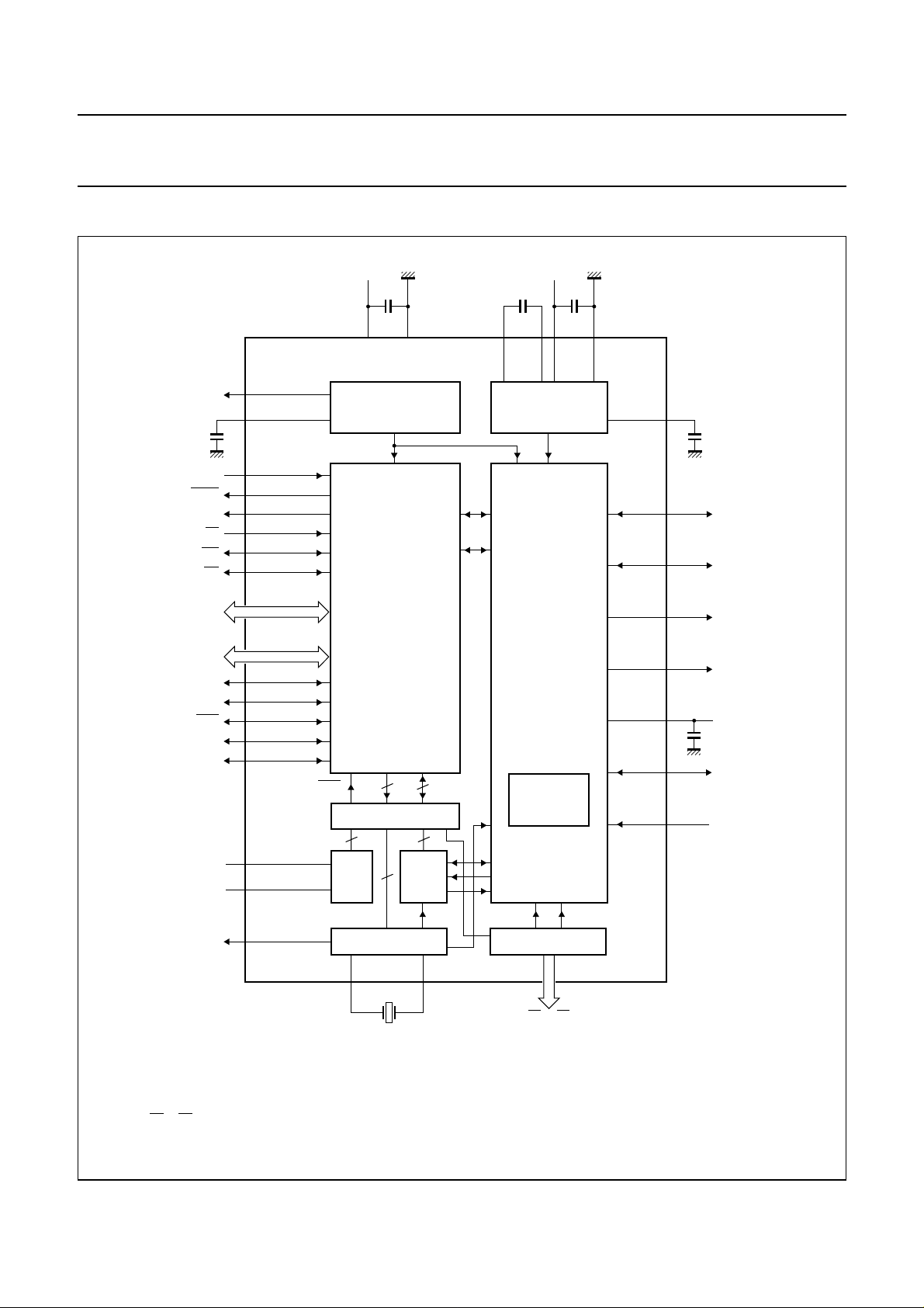
BLOCK DIAGRAM
handbook, full pagewidth
P00 to P07
P20 to P27
P11/T2EX
ALARM
CDELAY
RESET
PSEN
ALE
EA
P36/WR
P37/RD
P30/RXD
P31/TXD
P33/INT1
P10/T2
TDA8006H
(TDA8006AH)
45 (32)
44 (31)
52 (34)
7 (3)
8 (4)
11 (7)
61 (41)
62 (42)
19 to 12
(1)
(11 to 8)
63, 64, 1 to 6
(43, 44, 1, 2)
58 (38)
59 (39)
60 (40)
53 (35)
54 (36)
V
DD
100 nF
SUPPLY
AND
SUPERVISOR
MICROCONTROLLER
80C52
INT0
16-kbyte ROM
256-byte RAM
6
PERIPHERALS
(2)
100 nF
GND S1 S2
29 (19)41(28) 40 (27)
P34
P35
P40
8
to P47
(21)
CONVERTER
C4
C8
SEQUENCER
OSCILLATOR
V
DDA
31
30
(20)
STEP-UP
ANALOG
DRIVERS
AND
INTERNAL
AGND
28 (18)
(22) 32
(25) 38
(26) 39
(17) 27
(16) 26
(23) 36
(24) 37
(29) 42
VUP
100 nF
C4
C8
CLK
RST
V
CC
I/O
PRES
V
DDRAM
GNDRAM
CLKOUT
Minimum value for capacitor between V
Pin numbers in parenthesis represent the TDA8006AH.
(1) Ports P04 to P07 not applicable for QFP44 package.
(2) Ports P24 to P27 not applicable for QFP44 package.
(3) Ports K0 to K3 not applicable for QFP44 package.
23 (14)
24 (15)
43 (30)
1024
AUX
RAM
CLOCK CIRCUITRY PORT EXTENSION
10 (6)
XTAL1
and AGND is 2.2 µF.
DDA
T = 0,1
ISO
UART
9 (5)
XTAL2
Fig.1 Block diagram.
2000 Oct 30 4
I/O
OFF
3 V/5 V
CMDVCC
K0 to K3
48 to 51
(3)
MGR225
Page 5

Philips Semiconductors Product specification
Multiprotocol IC Card coupler TDA8006
PINNING
SYMBOL
DESCRIPTION
QFP64 QFP44
P22 1 1 address 10/general purpose I/O port
P23 2 2 address 11/general purpose I/O port
P24 3 − address 12/general purpose I/O port
P25 4 − address 13/general purpose I/O port
P26 5 − address 14/general purpose I/O port
P27 6 − address 15/general purpose I/O port
PSEN 7 3 program store enable output
ALE 8 4 address latch enable
XTAL2 9 5 crystal connection
XTAL1 10 6 crystal connection or external clock input
EA 11 7 external access
P07 12 − address/data 7/general purpose I/O port
P06 13 − address/data 6/general purpose I/O port
P05 14 − address/data 5/general purpose I/O port
P04 15 − address/data 4/general purpose I/O port
P03 16 8 address/data 3/general purpose I/O port
P02 17 9 address/data 2/general purpose I/O port
P01 18 10 address/data 1/general purpose I/O port
P00 19 11 address/data 0/general purpose I/O port
n.c. 20 12 not connected
n.c. 21 13 not connected
n.c. 22 − not connected
PIN
V
DDRAM
23 14 supply voltage for the auxiliary RAM
GNDRAM 24 15 ground for the auxiliary RAM
n.c. 25 − not connected
RST 26 16 card reset output (ISO contact C2)
CLK 27 17 clock output to the card (ISO contact C3)
AGND 28 18 ground for the analog part
S1 29 19 contact 1 for the step-up converter (a ceramic capacitor of 100 nF must be
connected between S1 and S2)
V
DDA
30 20 analog supply voltage for the voltage doubler
S2 31 21 contact 2 for the step-up converter (a ceramic capacitor of 100 nF must be
connected between S1 and S2)
VUP 32 22 output of the step-up converter; must be decoupled with a 100 nF ceramic
capacitor
n.c. 33 − not connected
n.c. 34 − not connected
n.c. 35 − not connected
V
CC
36 23 card supply output voltage (ISO contact C1)
2000 Oct 30 5
Page 6

Philips Semiconductors Product specification
Multiprotocol IC Card coupler TDA8006
SYMBOL
I/O 37 24 data line to/from the card (ISO contact C7)
C4 38 25 auxiliary I/O for ISO contact C4 (synchronous cards for example)
C8 39 26 auxiliary I/O for ISO contact C8 (synchronous cards for example)
GND 40 27 ground
V
DD
PRES 42 29 card presence contact input (active HIGH or LOW by mask option); see Table 12
CLKOUT 43 30 output for clocking external devices
CDELAY 44 31 external capacitor connection for delayed reset signal
ALARM 45 32 open drain reset output (active HIGH or LOW by mask option); see Table 12
TEST 46 33 test pin (must be left open-circuit in the application)
INHIB 47 − test pin (must be left open-circuit in the application)
K0 48 − output port from port extension (±2 mA push-pull)
K1 49 − output port from port extension (±2 mA push-pull)
K2 50 − output port from port extension (±2 mA push-pull)
K3 51 − output port from port extension (±2 mA push-pull)
RESET 52 34 input for resetting the microcontroller (active HIGH)
P10/T2 53 35 general purpose I/O port (connected to P10)
P11/T2EX 54 36 general purpose I/O port (connected to P11)
n.c. 55 37 not connected
n.c. 56 − not connected
n.c. 57 − not connected
P30/RXD 58 38 general purpose I/O port or serial interface receive line
P31/TXD 59 39 general purpose I/O port or serial interface transmit line
INT1 60 40 general purpose I/O port or interrupt (connected to P33)
P33/
P36/
WR 61 41 general purpose I/O port or external data memory write strobe
RD 62 42 general purpose I/O port or external data memory read strobe
P37/
P20 63 43 address 8/general purpose I/O port
P21 64 44 address 9/general purpose I/O port
QFP64 QFP44
PIN
DESCRIPTION
41 28 supply voltage
2000 Oct 30 6
Page 7
Philips Semiconductors Product specification
Multiprotocol IC Card coupler TDA8006
handbook, full pagewidth
P22
P23
P24
P25
P26
P27
PSEN
ALE
XTAL2
XTAL1
EA
P07
P06
P05
P04
P03
P02
P01
P00
P21
64
1
2
3
4
5
6
7
8
9
10
11
12
13
14
15
16
17
18
19
P20
63
P37/RD
62
61
P36/WR
P33/INT1
60
P30/RXD
P31/TXD
59
58
TDA8006H
n.c.
57
n.c.
56
n.c.
55
P11/T2EX
P10/T2
54
53
RESET
52
51
50
49
48
47
46
45
44
43
42
41
40
39
38
37
36
35
34
33
K3
K2
K1
K0
INHIB
TEST
ALARM
CDELAY
CLKOUT
PRES
V
DD
GND
C8
C4
I/O
V
CC
n.c.
n.c.
n.c.
20
21
22
23
24
25
n.c.
n.c.
n.c.
DDRAM
V
n.c.
GNDRAM
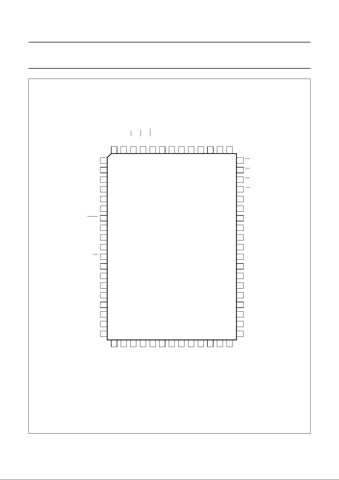
Fig.2 Pin configuration (QFP64).
2000 Oct 30 7
26
RST
27
CLK
28
AGND
29
S1
30
DDA
V
31
S2
32
VUP
MGR226
Page 8
Philips Semiconductors Product specification
Multiprotocol IC Card coupler TDA8006
handbook, full pagewidth
P20
P37/RD
P36/WR
P33/INT1
P31/TXD
P30/RXD
P11/T2EX
P10/T2
P21
44
n.c.
43
42
41
40
39
38
37
RESET
36
35
34
P22
P23
PSEN
ALE
XTAL2
XTAL1
EA
P03
P02
P01
P00
22
VUP
33
TEST
ALARM
32
31
CDELAY
30
CLKOUT
PRES
29
V
28
GND
27
C8
26
C4
25
24
I/O
V
23
MGR227
DD
CC
1
2
3
4
5
6
7
8
9
10
11
12
13
n.c.
n.c.
TDA8006AH
14
15
DDRAM
V
GNDRAM
16
RST
17
CLK
18
AGND
19
S1
20
DDA
V
21
S2
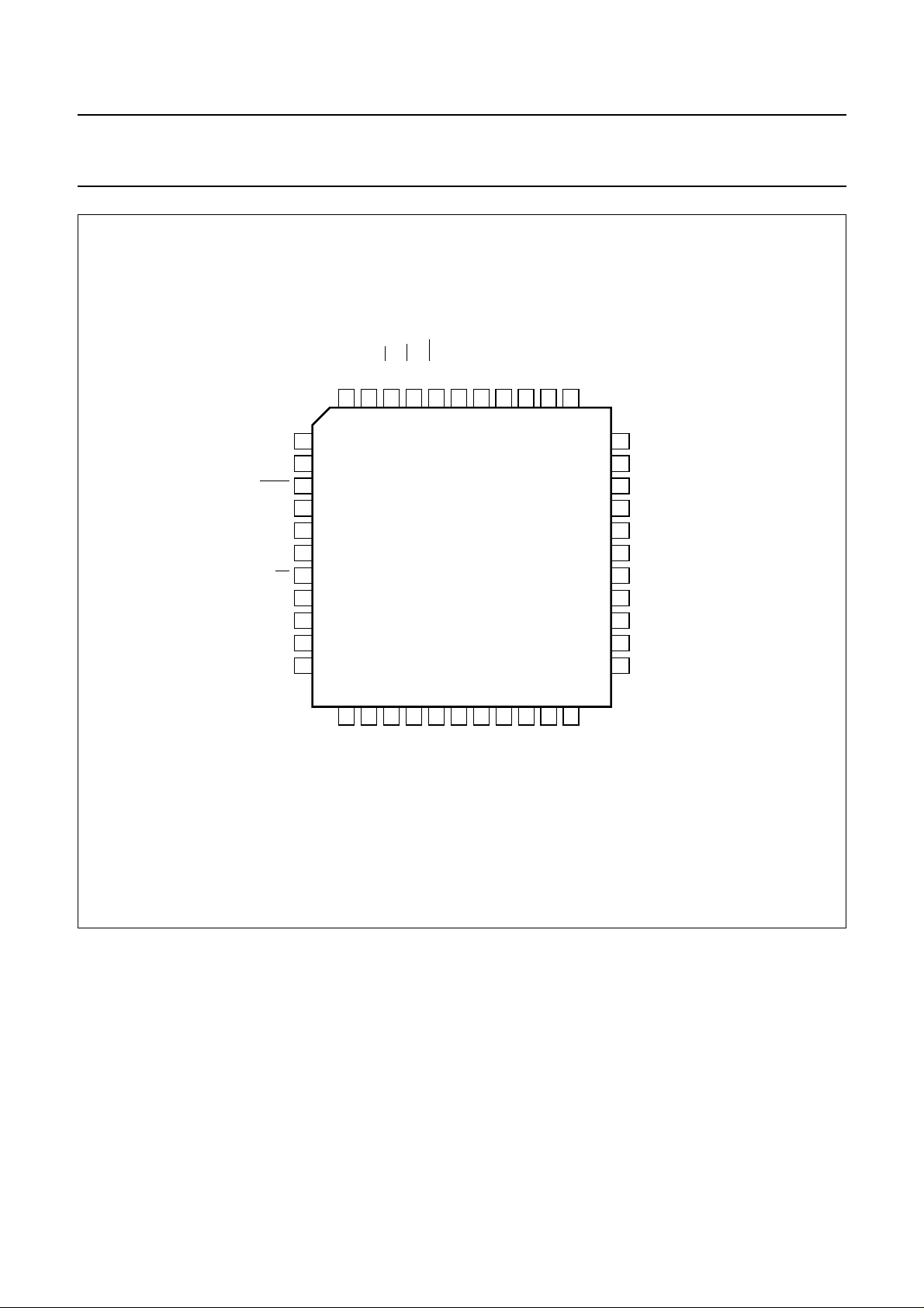
Fig.3 Pin configuration (QFP44).
2000 Oct 30 8
Page 9

Philips Semiconductors Product specification
Multiprotocol IC Card coupler TDA8006
FUNCTIONAL DESCRIPTION
Microcontroller
The microcontroller is an 80C52 with 16 kbytes of ROM,
256 byte RAM, timers 0, 1, 2 , and 5 I/O ports (port P0:
open-drain; ports P1 to P3: weak pull-up). Port P4 is
identical to 83CE560, except that precharge circuits
ensurefastrisetimesatend of read mode (transition times
<0.5 µs). The ROM code content can be tested by
signature to avoid reading it out after masking; for security
bit option, see Table 12. The CPU, timers 0 and 1, serial
UART, parallel I/O ports, 256 byte RAM, 16 kbyte ROM
and external bus are conventional C51 family library
elements. Timer 2 is a conventional C52 element
(interrupt enable bit ET2: bit 3 in register IEN1 at byte
address E8H and interrupt priority bit PT2: bit 3 in register
IP1 at byte address F8H.
Table 1 List of differences between TDA8006, CE560, CL580 and C52
FEATURES TDA8006 83CE560 CL580 INTEL C52
P4 address C0 C0 C1 no
Timer 2 Intel Philips Intel Intel
ROM size 16 kbytes 64 kbytes 6 kbytes 8 kbytes
External 0 interrupt vector 0003H 0003H 0003H 0003H
External 0 interrupt priority highest (1st) highest (1st) highest (1st) highest (1st)
Timer 0 interrupt vector 000BH 000BH 000BH 000BH
Timer 0 interrupt priority 2nd 2nd 4th 2nd
External 1 interrupt vector 0013H 0013H 0013H 0013H
External 1 interrupt priority 3th 3th 7th 3th
Timer 1 interrupt vector 001BH 001BH 001BH 001BH
Timer 1 interrupt priority 4th 4th 10th 4th
Serial 0 interrupt vector 0023H 0023H 0023H 0023H
Serial 0 interrupt priority 5th 5th 13th 5th
Timer 2 interrupt vector 004BH 0033H, etc. (8) 0033H 002BH
Timer 2 interrupt priority lowest (6th) miscellaneous 5th lowest (6th)
2
I
C-bus no yes yes no
ADC no yes yes no
32 kHz oscillator no yes no no
PWM no yes yes no
Watchdog no yes yes no
Interrupts on P1 no no yes no
Additional RAM 1 kbyte peripheral 2 kbyte MOVX no no
Wake-up from
power-down mode
reset,
INT0, INT1 reset, INT0,
INT1 + other
Register PCON has an added feature: PCON.5 = RFI
(reduced Radio Frequency Interference bit). When set to
logic 1, pin ALE cannot be toggled. ALE clears on RESET.
If access is required to the external data memory via
MOVXinstructions (see Table 1),setbit PCON.6 = ARD in
the PCON register to logic 1.
For further information, please refer to the published
specification of the 83CE560 in
80C51-Based 8-Bit Microcontrollers”
PortsP40 to P47, INT0 and P12 to P17 areusedinternally
for controlling the smart card interface and the other
peripherals. Ports P34 and P35 are used to control the
auxiliary contacts C4 and C8.
The list of differences given in Table 1 may help the
software developer of the dedicated emulation board for
the TDA8006 or other devices.
reset, INT2 to INT8 reset
“Data Handbook IC20;
.
2000 Oct 30 9
Page 10

Philips Semiconductors Product specification
Multiprotocol IC Card coupler TDA8006
Table 2 Special function register bit addresses
X = don’t care.
BYTE
REGISTER
IP1 F8 [FF] [FE] [FD] [FC] [FB] [FA] [F9] [F8]
B F0 [F7] [F6] [F5] [F4] [F3] [F2] [F1] [F0]
IEN1 E8 [EF] [EE] [ED] [EC] [EB] [EA] [E9] [E8]
ACC E0 [E7] [E6] [E5] [E4] [E3] [E2] [E1] [E0]
PSW D0 [D7] [D6] [D5] [D4] [D3] [D2] [D1] [D0]
T2CON C8 [CF] [CE] [CD] [CC] [CB] [CA] [C9] [C8]
P4 C0 [C7] [C6] [C5] [C4] [C3] [C2] [C1] [C0]
IP0 B8 [BF] [BE] [BD] [BC] [BB] [BA] [B9] [B8]
P3 B0 [B7] [B6] [B5] [B4] [B3] [B2] [B1] [B0]
IEN0 A8 [AF] [AE] [AD] [AC] [AB] [AA] [A9] [A8]
P2 A0 [A7] [A6] [A5] [A4] [A3] [A2] [A1] [A0]
SCON 98 [9F] [9E] [9D] [9C] [9B] [9A] [99] [98]
P1 90 [97] [96] [95] [94] [93] [92] [91] [90]
TCON 88 [8F] [8E] [8D] [8C] [8B] [8A] [89] [88]
P0 80 [87] [86] [85] [84] [83] [82] [81] [80]
ADDRESS
(HEX)
MSB LSB
−−−−PT2 −−− XXXX 0XXX
−−−−−−−− 0000 0000
−−−−ET2 −−− 0000 0000
−−−−−−−− 0000 0000
CY AC F0 RS1 RS0 OV F1 P 0000 0000
TF2 EXF2 RCLK TCLK EXEN2 TR2 C/T2N CP/RL2N 0000 0000
−−−−−−−− 1111 1111
−−−PS0 PT1 PX1 PT0 PX0 XXX0 0000
−−−−−−−− 1111 1111
EA −−ES0 ET1 EX1 ET0 EX0 0XX0 0000
−−−−−−−− 1111 1111
SM0 SM1 SM2 REN TB8 RB8 TI RI 0000 0000
−−−−−−−− 1111 1111
TF1 TR1 TF0 TR0 IE1 IT1 IE0 IT0 0000 0000
−−−−−−−− 1111 1111
BIT ADDRESS [HEX]
BIT FUNCTION
BIT RESET
VALUE
2000 Oct 30 10
Page 11
Philips Semiconductors Product specification
Multiprotocol IC Card coupler TDA8006
Table 3 Other register byte addresses
REGISTER
BYTE
ADDRESS
(HEX)
BIT RESET
VALUE
SP 81 0000 0111
DPL 82 0000 0000
DPH 83 0000 0000
PCON 87 0000 0000
TMOD 89 0000 0000
TL0 8A 0000 0000
TL1 8B 0000 0000
TH0 8C 0000 0000
TH1 8D 0000 0000
S0BUF 99 XXXX XXXX
RCAP2L CA 0000 0000
RCAP2H CB 0000 0000
TL2 CC 0000 0000
TH2 CD 0000 0000
Supply
The circuit operates within a supply voltage range of
4.2 to 6 V. The supply pins are VDD, V
V
and GNDRAM. Pins V
DDRAM
and AGND supply the
DDA
, GND, AGND,
DDA
card analog drivers and have to be externally decoupled
because of the large current spikes that the card and the
step-up converter can create. V
and GNDRAM
DDRAM
supply the auxiliary RAM and should be decoupled
separately. VDD and GND supply the rest of the chip.
An integrated spike killer ensures the contacts to the card
remain inactive during power-up or power-down.
An internally generated voltage reference is used by the
step-up converter, the voltage supervisor and the V
CC
generator.
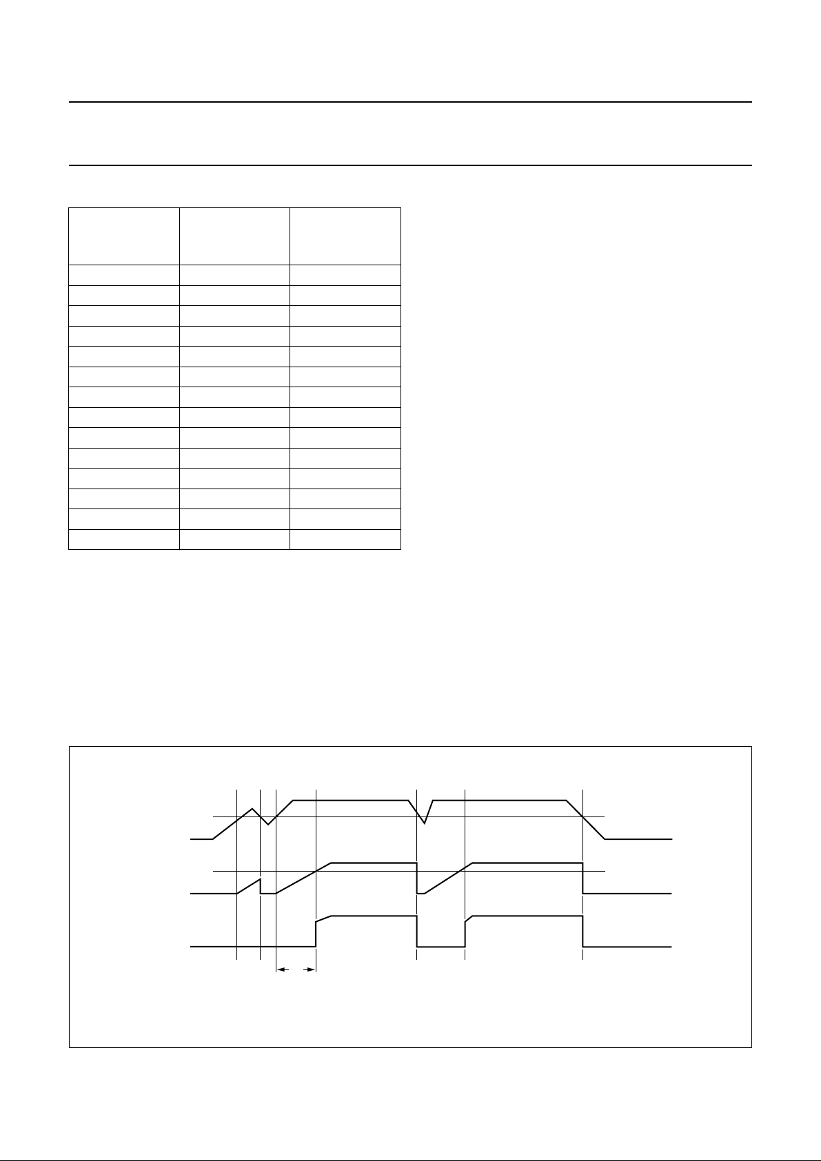
If VDD is too low to ensure proper operation, the voltage
supervisor generates an alarm pulse, whose length is
defined by an external capacitor tied to the CDELAY pin,
(1 ms per 1 nF typical). This pulse is used to reset the
controller and is used in parallel with an external reset
input which can come from the system controller. It is also
used to either block any spurious on-card contacts during
a controller reset or to force an automatic deactivation of
the contacts in the event of supply drop-out (see
Sections “Activation sequence” and “Deactivation
sequence”). It is also fed to an external open-drain output
(calledALARM)whichcanbe chosen active HIGH or LOW
by mask option (see Table 12).
Step-up converter
Except for the VCC generator and the other card contact
buffers, the whole circuit is powered by VDD, V
V
. If the supply voltage is 4.2 V, then a higher
DDRAM
DDA
and
voltageisneededforthesupply to the ISO contacts. When
a card session is requested by the controller, the
sequencer first starts the step-up converter. This uses
switched capacitors which are clocked at a frequency of
approximately 2.5 MHz by an internal oscillator.
The output voltage VUP is regulated at approximately 6 V
and then fed to the VCCgenerator. VCCand GND are used
as a reference for all other card contacts.
handbook, full pagewidth
V
DD
CDELAY
ALARM
t
W
Fig.4 Voltage supervisor.
2000 Oct 30 11
V
th(VDD)
V
th(CDELAY)
MGR228
Page 12
Philips Semiconductors Product specification
Multiprotocol IC Card coupler TDA8006
ISO 7816 security
Thecorrectsequence during activation and deactivationof
the card is ensured by a specific sequencer clocked at a
frequency which is a division ratio of the internal oscillator.
Activation(bit CMDVCC within the portsextensionregister
HIGH) is only possible if the card is present (pin PRES
HIGH or LOW according to the mask option) and if the
supply voltage is correct (ALARM signal inactive).
The presence of the card is signalled to the controller by
the OFF bit (within the UART status register), generating
an interrupt, if enabled, when toggling.
During a session, the sequencer performs an automatic
emergency deactivation in the event of card take-off,
supply voltage drop or short circuit. The OFF bit goes
LOW, thereby warning the controller through the interrupt
line INT0 and the status register.
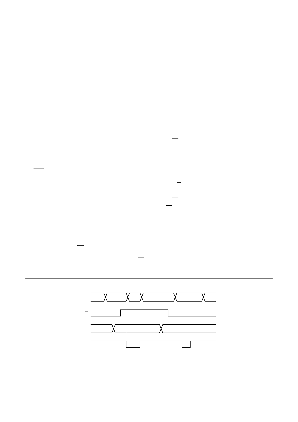
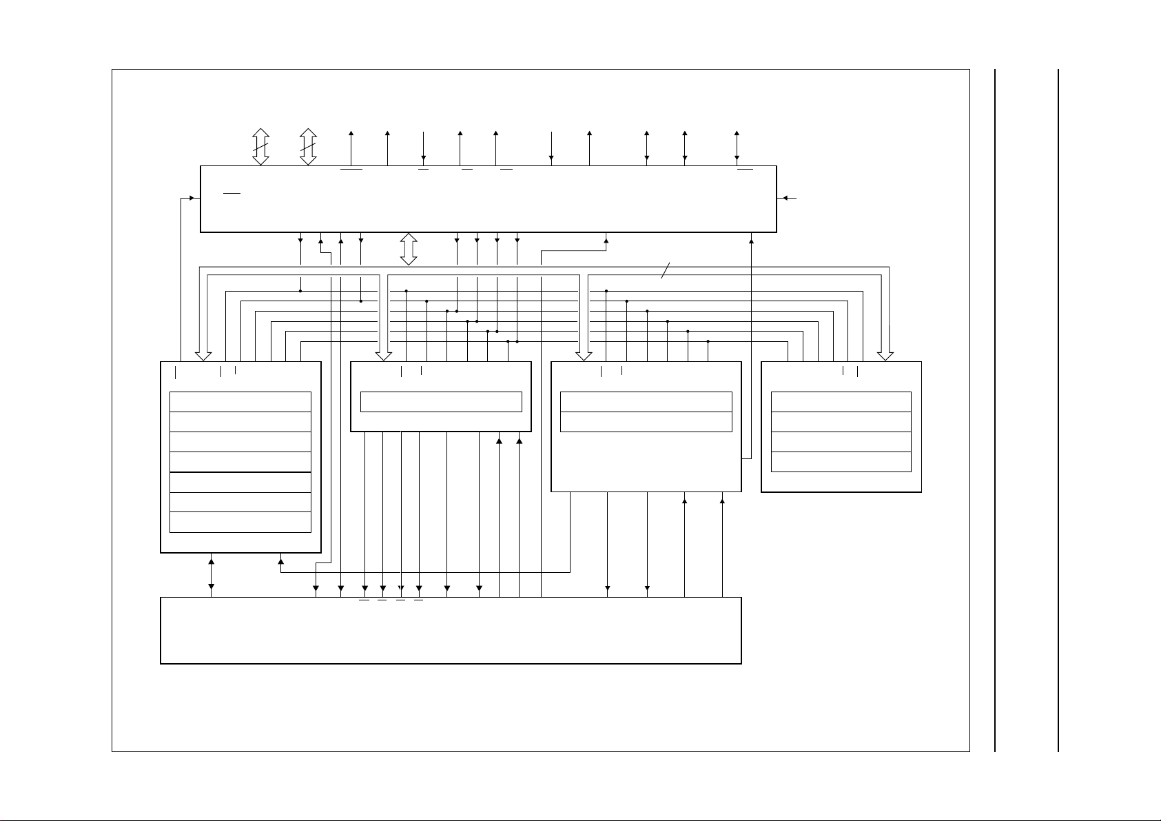
Peripheral interface (see Figs 5 and 6) This block allows parallel communication with the four
peripherals (ISO 7816 UART, clock generator, on/off
sequencer and auxiliary RAM) through an 8-bit data bus,
6-bit address and control bus and one interrupt line to the
controller. The data bus consists of ports P40 (data bit 0)
to P47 (data bit 7). The address bus consists of ports AD0
(P12), AD1 (P13), AD2 (P14) and AD3 (P15). The control
lines are R/W (P16) and EN (P17). The interrupt line is
INT0.
After resetting EN HIGH, the controller must release the
bus by setting port P4 HIGH again (the transition times on
port P4 are less than 500 ns).
The interrupt line is reset HIGH when reading out the
status register.
READ OPERATION
• Set port P4 to FFH
• Select the register with AD0, AD1, AD2, AD3
• Assert R/W HIGH
• Assert EN LOW; the data is available on data bus P4
• Read the data on port P4
• Set EN HIGH; the bus is set to high impedance.
WRITE OPERATION
• Select the correct register with AD0, AD1, AD2, AD3
• Assert R/W LOW
• Write data to the data bus port P4
• Assert EN LOW; the data is written to the register
• Set EN HIGH
• Set port P4 to FFH; the bus is set to high impedance.
Integrated precharges allow fast rising edges on port P4
when changing from read mode to write mode, thus
avoiding the need to trigger the active pull-ups on port P4.
During a read operation, EN goes LOW allowing the
controllertoreaddata on the bus. During awriteoperation,
the data should be present on the bus before asserting EN
LOW which allows the data to be written to the registers.
handbook, full pagewidth
P4 XX FF FF FFDATA
R/W
AD0 to AD3 X AD AD
EN
read data cycle write data cycle
Fig.5 Use of peripheral interface.
2000 Oct 30 12
DATA
MGR229
Page 13
This text is here in white to force landscape pages to be rotated correctly when browsing through the pdf in the Acrobat reader.This text is here in
_white to force landscape pages to be rotated correctly when browsing through the pdf in the Acrobat reader.This text is here inThis text is here in
white to force landscape pages to be rotated correctly when browsing through the pdf in the Acrobat reader. white to force landscape pages to be ...
2000 Oct 30 13
handbook, full pagewidth
Philips Semiconductors Product specification
Multiprotocol IC Card coupler TDA8006
8
P00/P07
P32/INT0
INT
SYNCHRONOUS IN REGISTER
SYNCHRONOUS OUT REGISTER
CONFIGURATION REGISTER
EN
R/W
TRANSMIT REGISTER
RECEIVE REGISTER
STATUS REGISTER
GUARD TIME REGISTER
ISO 7816 UART
8
P20/P27 ALE
P17
AD3
AD2
AD1
PSEN EA P37/RD P36/WR P33/INT1P30/RXD P31/TXD P10/T2 P11/T2EX
80C52 CORE
P15 P14 P13 P12P40 to P47P34 P35 P16 OSC
AD0
EN
R/W
AD3
AD2
AD1
PERIPHERAL EXTENSION REGISTER
ON/OFF SEQUENCER
AD0
UART
CLOCK
EN
CLOCK CONFIGURATION REGISTER
PROGRAMMABLE DIVIDER
CLOCK GENERATOR
CARD
CLOCK
R/W
AD3
EXTERNAL
CLOCK
8
AD2
AD1
MICRO CLOCK
AD0
XTAL
RESET
databus
control bus
AD0
LOW ADDRESS REGISTER
HIGH ADDRESS REGISTER
MEMORY READ REGISTER
MEMORY WRITE REGISTER
R/W
AD3
AD2
AD1
AUXILIARY RAM
EN
MGR230
I/O C4 C8 K0 K1
INTERFACE, SECURITY AND POWER CONTROL
K2 K3
RST DET ERR POR CLK CLKOUT OSCINT XTAL1
CMDVCC
Fig.6 Peripheral interface.
Page 14

Philips Semiconductors Product specification
Multiprotocol IC Card coupler TDA8006
Table 4 Register addresses
X = don’t care.
AD3 AD2 AD1 AD0 R/
W REGISTER PERIPHERAL
00000CCR (Clock Configuration Register) clock generator
00010PDR (Programmable Divider Register)
00110SOR (Synchronous Output Register) ISO 7816 UART
00111SIR (Synchronous Input Register)
01000UTR (UART Transmit Register)
01001URR (UART Receive Register)
01011USR (UART Status Register)
01010UCR (UART Configuration Register)
01100GTR (Guard Time Register)
01110PER (Ports Extension Register) on/off sequencer
1 1 0 X 0 MAR0 (Memory Address LOW) auxiliary RAM
1 1 1 X 0 MAR1 (Memory Address HIGH)
1 0 0 X 0 MWR (Memory Write Register)
1 0 0 X 1 MRR (Memory Read Register)
Clock circuit
The microcontroller clock (OSC), the card clock (CLK), the
ISO 7816 UART clock, and the clock to the external world
(CLKOUT), are derived from the main clock signals (XTAL
from 4 to 20 MHz, or an external clock signal applied to
XTAL1), or the internal oscillator (f
INT
).
• Microcontrollerclock(OSC):afterpower-onor reset, the
microcontrollerisclocked at1⁄8f
may decide to clock it at1⁄2f
.Then,the application
INT
,1⁄2f
xtal
or f
xtal
INT
.
To achieve the different I/O baud rates as defined by
values F and D (see Table 7), the clock signal is counted
by an auto-reload 8-bit programmable counter and then
divided by a 31 or 32 prescaler.
All these configurations are controlled by the clock
configuration register and by the programmable divider
register.
All frequency changes are synchronous, thereby
ensuring no hang-up due to short spikes etc.
• Card clock (CLK): the application may send a clock
frequency of1⁄2f
xtal
,1⁄4f
xtal
,1⁄8f
xtal
or1⁄2f
(≈1.25 MHz),
INT
or may stop the clock at HIGH or LOW. All transitions
are synchronous, ensuring correct pulse length during
start or change, in accordance with ISO 7816. After
power-on or reset, CLK is held LOW.
• External clock output (CLKOUT): CLKOUT is a
permanent clock output for external use. The following
frequencies are possible: f
xtal
,1⁄2f
and1⁄4f
xtal
xtal
.
All transitions are synchronous. After power-on or reset,
CLKOUT is fixed at1⁄4f
xtal
.
• ISO 7816 UART clock: the clock to the ISO 7816 UART
is identical to the clock to the card (CLK).
2000 Oct 30 14
Page 15
Philips Semiconductors Product specification
Multiprotocol IC Card coupler TDA8006
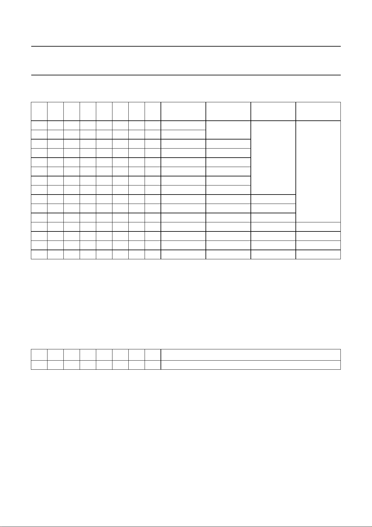
Table 5 Clock Configuration Register (CCR; address 0; write only; all bits cleared after reset)
X = don’t care.
D7 D6 D5 D4 D3 D2 D1 D0
UART
PRESCALER
CLK CLKOUT OSC
XXXXXXX0÷31
XXXXXXX1÷32
XXXX000X STOPLOW
XXXX001X
XXXX010X
XXXX011X
XXXX100X
1
⁄2f
xtal
1
⁄4f
xtal
1
⁄8f
xtal
1
⁄2f
INT
XXXX101X STOPHIGH
XX00XXXX
XX01XXXX f
XX10XXXX
00XXXXXX
01XXXXXX f
10XXXXXX
11XXXXXX
1
⁄4f
xtal
xtal
1
⁄2f
xtal
1
⁄8f
INT
xtal
1
⁄2f
xtal
1
⁄2f
INT
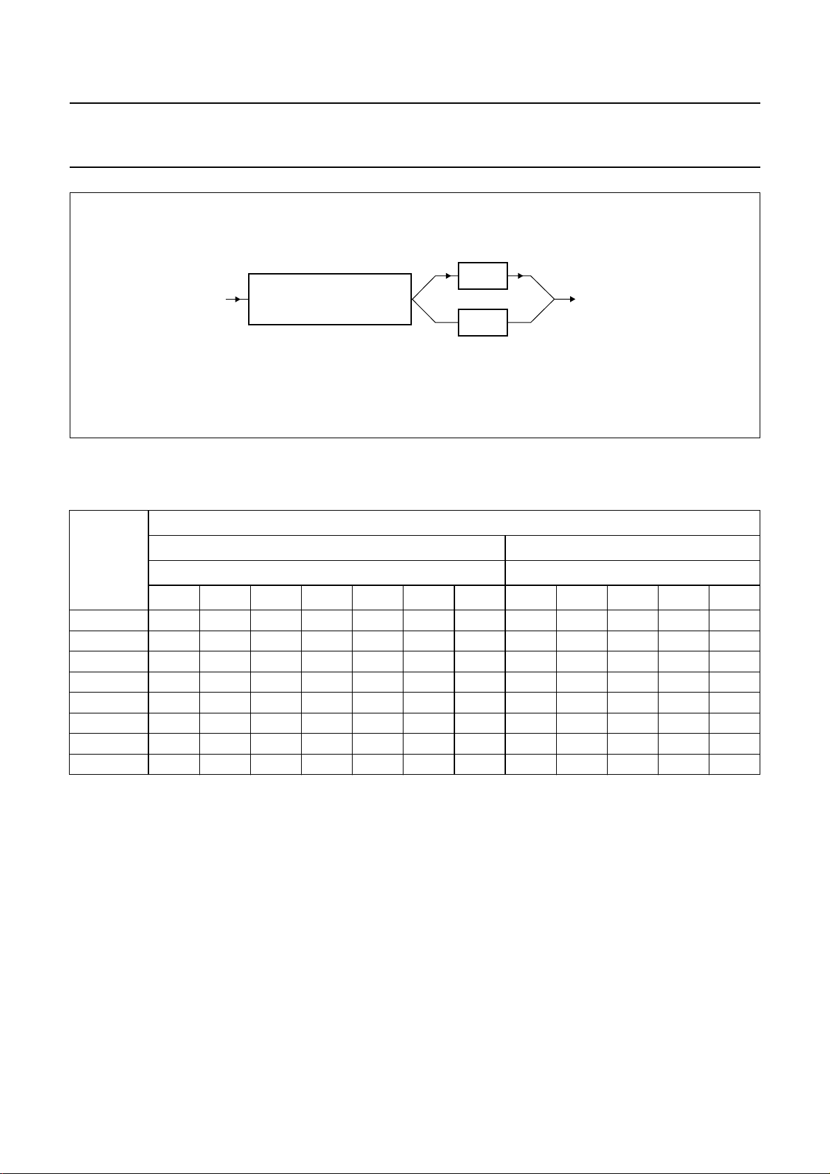
The hexadecimal value stored in the Programmable Divider Register (PDR) is the auto-reload value of an 8-bit counter
clocked by the card clock (CLK); when the value is loaded in the counter, it counts from this value till overflow; then it is
reloaded with the same value and the count restarts. The output of the counter is then divided by 31 or 32 depending on
the programmed value of the UART prescaler. The result is the ISO 7816 UART CLK which is used for shifting the data
in or out on the I/O line.
The example shown in Fig.7 shows how to program a division factor of 372. With these registers, the baud rates given
in Table 7 are achieved according to ISO 7816. The division ratio of 31 or 32 depends on which prescaler is selected,
and the hexadecimal value is the value programmed within the PDR.
Table 6 Programmable Divider Register (PDR; address 1; write only; all bits cleared after reset)
D7 D6 D5 D4 D3 D2 D1 D0 DIVISION FACTOR
n7 n6 n5 n4 n3 n2 n1 n0 n7n6n5n4 n3n2n1n0
(1)
Note
1. A division factor of F4H, for example, would be 1111 0100 reading from D7 to D0.
2000 Oct 30 15
Page 16
Philips Semiconductors Product specification
Multiprotocol IC Card coupler TDA8006
handbook, full pagewidth
CLK
8-BIT AUTO-RELOAD COUNTER
WITH PDR = F4H
÷31
ISO 7816
UART CLK
÷32
MGR231
Fig.7 Baud rate selection on I/O.
Table 7 Selecting baud rate using F and D values
Baud rate is selected by values D and F shown in parenthesis. The PDR is loaded with a value shown in Hexadecimal,
and either prescaler 31 or 32 is selected.
PDR VALUE
PRESCALER ÷31 PRESCALER ÷32
[VALUE D]
[VALUE F] [VALUE F]
[0000] [0001] [0010] [0011] [0100] [0101] [0110] [1001] [1010] [1011] [1100] [1101]
[0001] F4 F4 EE E8 DC D0 C4 F0 E8 E0 D0 C0
[0010] FA FA F7 F4 EE E8 E2 F8 F4 F0 E8 E0
[0011] FD FD − FA F7 F4 F1 FC FA F8 F4 F0
[0100] −−−FD − FA − FE FD FC FA F8
[0101] −−−−−FD − FF − FE FD FC
[0110] −−−−−−−−−FF − FE
[1000] FF FF − FE FD FC FB − FE − FC −
[1001] −−−−−−FD −−−−−
2000 Oct 30 16
Page 17

Philips Semiconductors Product specification
Multiprotocol IC Card coupler TDA8006
On/off controller
Table 8 On/off controller bits (PER; address 7; write only; all bits cleared after reset)
BIT NAME DESCRIPTION
D0 CMDVCC; set and reset by software set to 1 for starting activation sequence of the card, and reset
to 0 for starting deactivation
D1 RSTIN; set and reset by software control line RST for card contact C2 in manual mode (active
HIGH)
D2 Force Inverse Parity (FIP); set and reset by
software
D3 automatic ATR processing enabling
(ATREN); set by software, reset by
hardware
D4
D5
D6
D7
K0; set and reset by software auxiliary ±2 mA push-pull output control (inverted output)
K1; set and reset by software auxiliary ±2 mA push-pull output control (inverted output)
K2; set and reset by software auxiliary ±2 mA push-pull output control (inverted output)
K3; set and reset by software auxiliary ±2 mA push-pull output control (inverted output)
when LOW, the UART processes the parity according to
ISO 7816; when HIGH, the UART processes the inverse parity
(which causes parity errors during transmission and ‘not
acknowledge’ signals during reception)
when HIGH, the UART automatically counts the clock pulses
during ATR and controls the RST contact; this bit is
automatically reset by hardware when a start bit is detected
on I/O or when the card is declared as mute; when LOW, this
automatic processing is disabled (manual mode)
The on/off controller is used for activating or deactivating
the card, for controlling contact C2 (RST) manually
through RSTIN or automatically, for forcing inverse parity
(for flow control or test purposes), and for controlling four
independent push-pull output lines K0 to K3.
After having cleared the ISO 7816 UART reset bit (see
UART configuration register) and checking the card
presence within the status register, the software may
initiate an activation sequence by setting bit CMDVCC
HIGH. It may also initiate a deactivation sequence by
resetting this bit (see activation and deactivation
sequences).
The timings during the ATR may be checked either
manually (using RSTIN and t3/t5for counting clock pulses)
or automatically by setting bit ATREN HIGH (see Section
“Activation sequence”). In this case, hardware controls
both RST and the counting of CLK pulses. Bit ATREN is
reset by hardware when a start bit has been detected
before 2 × 40100 CLK pulses for versions C2 and C3
(2 × 45000 CLK pulses for version C1), or when the card
is declared as ‘mute’. Setting this bit HIGH again during a
session initiates a warm reset.
A warm reset may also be done manually by using RSTIN
and t3/t5 again.
ISO 7816 UART
The ISO 7816 UART handles all specific requirements
defined in ISO 7816 T = 0 and T = 1 protocol types. It is
also able to deal with synchronous cards (in conjunction
with contacts C4 and C8). In addition, there is a possibility
to force parity errors for test purposes or flow control.
The counting of CLK cycles during ATR is possible by
either hardware or software.
The ISO 7816 UART is configured with 2 registers: UART
Configuration Register (UCR) and Guard Time Register
(GTR).
When timings are given in terms of ETU (Elementary Time
Unit as defined by ISO 7816), then the reference is the
negative edge of the start bit of the character being
received or transmitted, unless otherwise specified.
2000 Oct 30 17
Page 18

Philips Semiconductors Product specification
Multiprotocol IC Card coupler TDA8006
Table 9 UART Configuration Register (UCR; address 5; write only; all bits cleared after reset)
BIT NAME DESCRIPTION
D0 Reset ISO 7816 UART (RIUN); set by
software, reset by software
D1 Start Session (SS); set by software, reset by
software
D2 Last Character to Transmit (LCT); set by
software, reset by hardware or software
D3 Transmit/Receive-N (TRN); set by software,
reset by software or hardware
D4 not used
D5 Protocol Selection (PS); set by software, reset
by software
D6 3 V/5 V-N (TFN); set by software, reset by
software
D7 Synchrone/asynchrone-N (SAN); set by
software, reset by software
when LOW, this bit resets the UART; must be set by software
before any use of the UART
when HIGH, this bit allows the detection of the convention
during the initial character of the card; must be reset by
software after correct reception of the first character and before
complete reception of the next character
when HIGH, this bit allowsautomatic toggling from transmission
to reception mode after successful transmission of the last
character; in this case, TRN is also reset by hardware
when LOW, the UART is in reception mode; when HIGH, it is in
transmission mode;
when LOW, the UART is in T = 0 mode; when HIGH, the UART
is in T = 1 mode
when LOW, the card supply voltage V
VCC=3V
when HIGH, this bit allows direct monitoring of I/O by bit D0 of
SIR or SOR; when LOW, I/O is fed to the ISO 7816 UART
INT goes LOW when TRN is set
= 5 V; when HIGH,
CC
RECEPTION
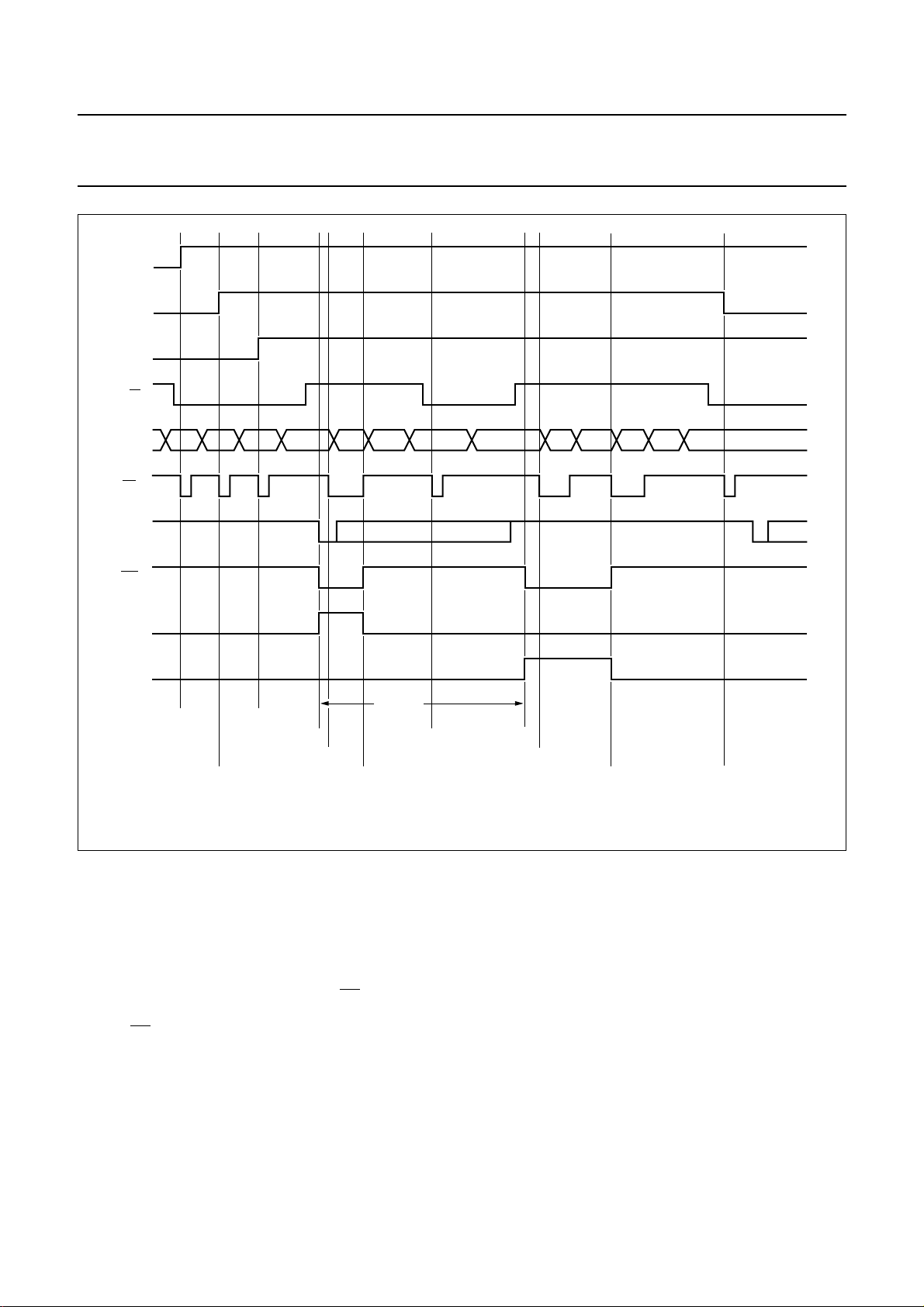
In order to start a session with the card, bit RIUN (which
resets the ISO 7816 UART when LOW) must be set HIGH.
The UART recognizes the convention (direct or inverse) of
the characters received while bit SS (Start Session) is
HIGH. Then the UART automatically converts any
transmitted or received character according to this
convention, so the software only has to deal with
characters written in direct convention. Indeed, bit SS
must be reset by software after correct receipt of the first
character of the ATR (TS) and before complete receipt of
the next character.
Reception mode is selected when TRN is LOW. Bit FSD is
set within the UART Status Register (USR), and an
interrupt is generated, if enabled, at the start bit of the
received character when SS is HIGH, allowing the manual
CLKcount during ATR. The interrupt will be cleared on the
rising edge of EN during the status read operation.
For the next characters, bit RBF is set at 10.5 ETU and an
interrupt is generated, if enabled, to indicate that a
character has been received, with or without parity error,
and that this character may be read within the reception
register. The interrupt is cleared on the falling edge of EN
during the read operation of the received character.
In protocol type T = 0 (bit PS LOW), the I/O line is
automatically pulled LOW between 10.5 and 11.75 ETU if
a character parity error is detected (parity error handling at
character level).
In protocol type T = 1 (bit PS HIGH), if a parity error is
detected,bit PEissetinthestatusregister,buttheI/O line
is not pulled LOW.
2000 Oct 30 18
Page 19
Philips Semiconductors Product specification
Multiprotocol IC Card coupler TDA8006
handbook, full pagewidth
RIU
SS
CMDVCC
R/W
P4 FF FF FF FF FF
EN
I/O
INT
FSD
RBF
release reset
set start session
set CMDVCC
first start
read status
10.5 ETU
anything
int cleared
Fig.8 First character reception.
TRANSMISSION
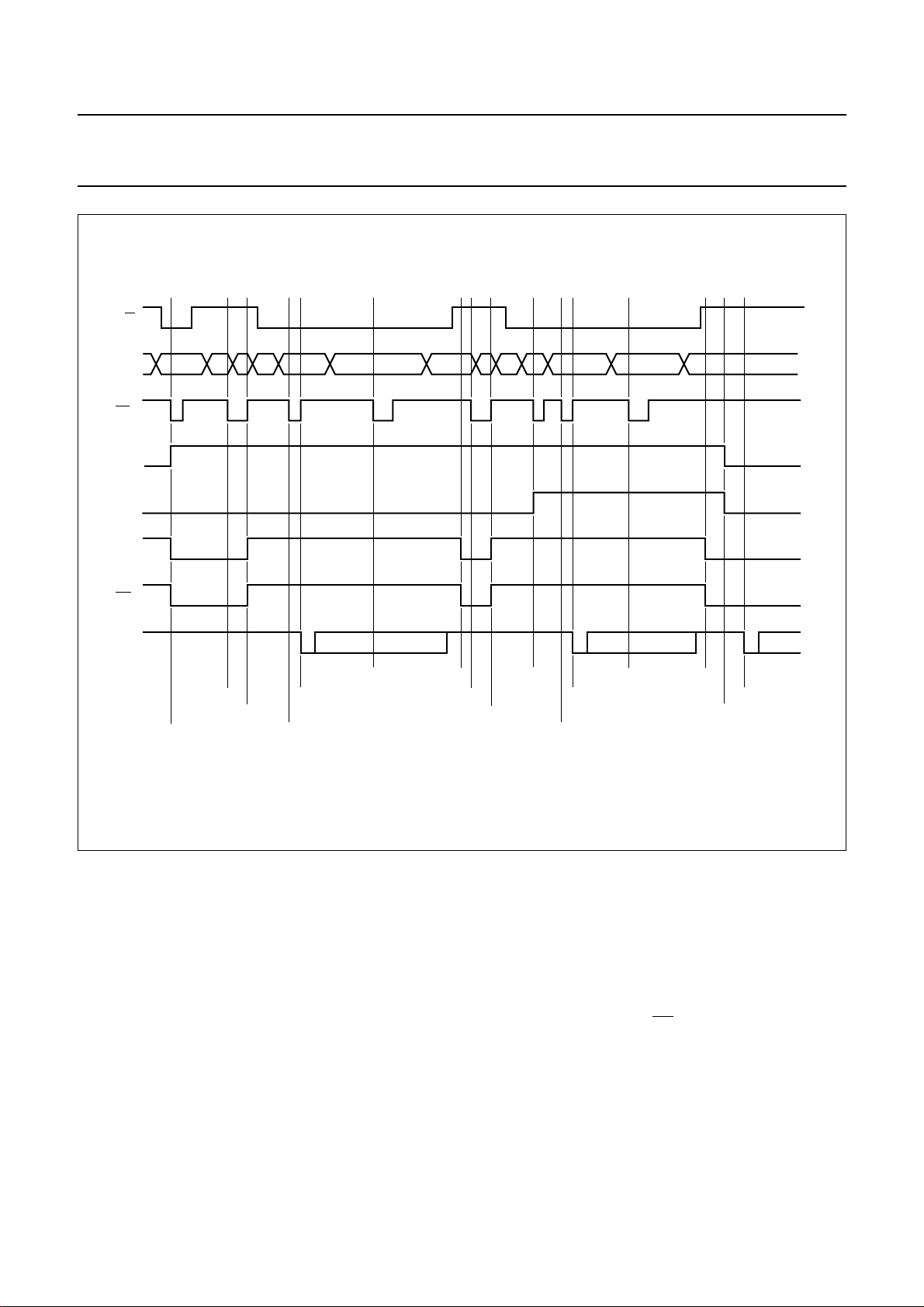
Transmission mode is selected when TRN is HIGH.
If enabled, an interrupt occurs on the rising edge of TRN,
indicating that the transmission buffer is empty and ready
to accept a character for transmission. The interrupt is
cleared during the read status operation. The character is
written to the UTR on the falling edge of EN during the
write operation, and starts to be transmitted on the rising
edge of EN.
The I/O line is read at 10.84 ETU to check if the card has
detected a parity error. At the same time, bit TBE is set in
the USR, and, if enabled, an interrupt occurs to indicate
that the transmission buffer is empty, and that a new
character may be written. If the parity is correct, the
transmission of the next character will start at
12 ETU + GT + 0.5 ETU after the start bit of the previous
buffer full
read status
read character
and int cleared
reset start session
MGR232
character (see Section “Extra guard time”). If the parity is
not correct, then assuming that a character has been
written to the UTR, the transmission starts at 13 ETU (the
guard time GT must be programmed before transmitting).
Bit LCT can be used for cards that are required to change
fromtransmissiontoreception mode very fast. If LCTisset
HIGH, then the UART automatically resets
bits TRN and LCT at 10.85 ETU if no parity error has
occurred; the UART is ready to receive a character from
the card at 12 ETU (T = 0) or 11 ETU (T = 1) after the
previous start bit. If a parity error has occurred during
transmission of the last character, then the UART stays in
transmission mode with LCT set, waiting for the software
to rewrite the corrupted character.
2000 Oct 30 19
Page 20
Philips Semiconductors Product specification
Multiprotocol IC Card coupler TDA8006
handbook, full pagewidth
R/W
P4 FF FF FFFF
EN
TRN
LCT
TBE
INT
I/O
anything buffer empty
read status start transmit read status
int cleared
transmission
write character
int cleared
set LCT
anything buffer empty
start transmit
write character
FF
start receive
TRN/LCT reset
MGR233
Fig.9 Character transmission with or without LCT.
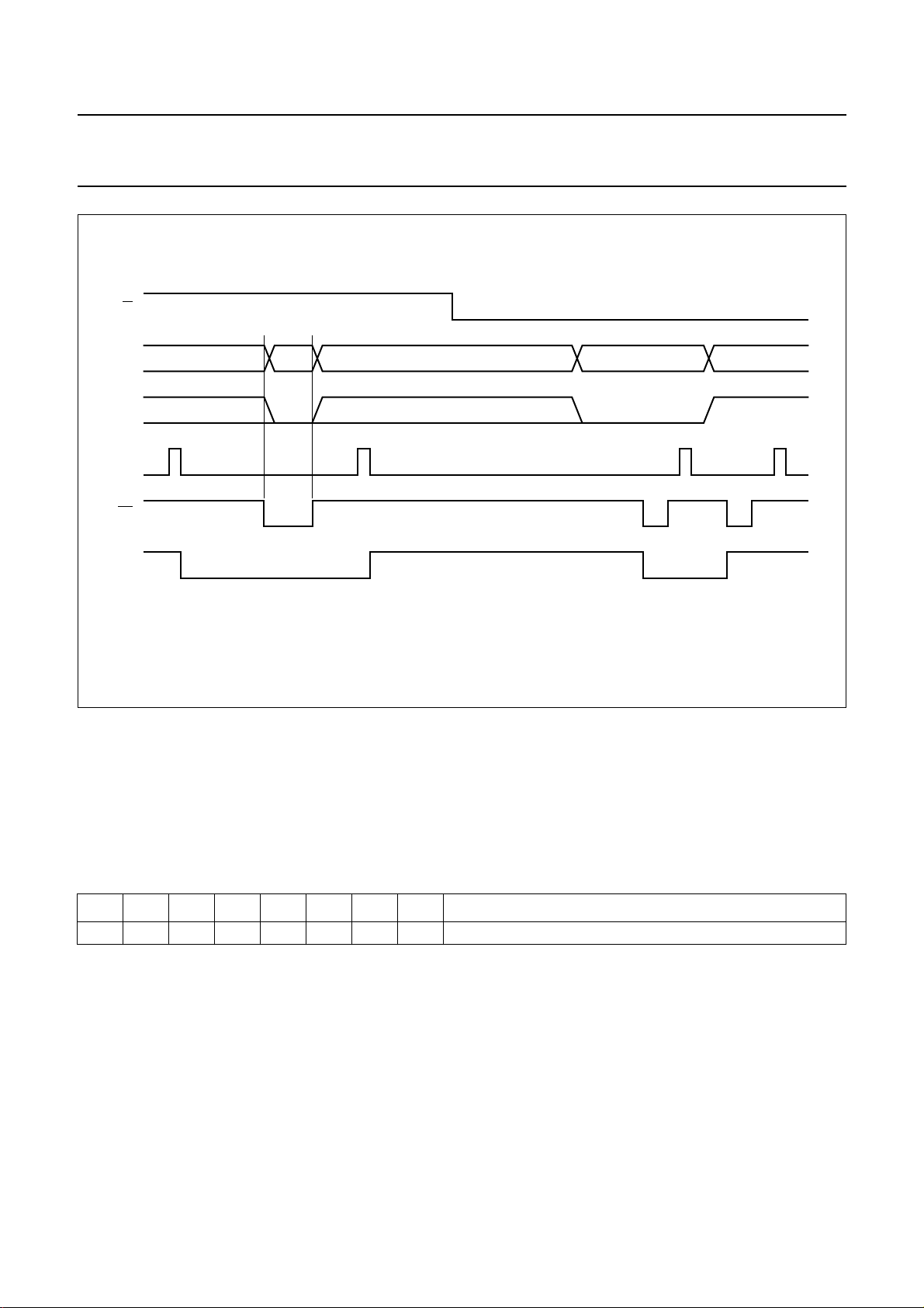
SYNCHRONOUS CARDS
If bit SAN (Synchronous/Asynchronous-N) is set, the
software can operate with synchronous cards; the
information available on the I/O line is copied on data bit 0
of the data bus without entering the UART when either
registers SIR or SOR are selected. At the end of a
transmission in synchronous mode, it is necessary to
switch back to synchronous reception mode by reading
register SIR.
The synchronous clock may be controlled by selecting
CLK STOP HIGH or STOP LOW. Contacts C4 and C8
may be controlled by ports P34 and P35 (operation
depends on synchronous card type).
2000 Oct 30 20
Synchronous Input Register (SIR; address 3; read only)
When this register is selected, I/O is copied on data bit 0
(P40) and may be read by the controller.
Synchronous Output Register (SOR; address 3; write
only)
When this register is selected, I/O is copied on data bit 0
(P40) on the falling edge of EN.
Page 21
Philips Semiconductors Product specification
Multiprotocol IC Card coupler TDA8006
handbook, full pagewidth
R/W
P4
P40
CLK
EN
I/O
FF FF
read write
Fig.10 Using synchronous cards.
EXTRA GUARD TIME
Between the transmission of two characters to the card,
the ISO 7816 UART automatically inserts a number of
guard ETUs equal to the value, called GT, stored in the
GTR, see Table 10. For a GT of FAH, for example, the
value would be 1111 1010 reading from D7 to D0.
MGR234
A GT of FFH has a special status which means 0 ETU
when the protocol is T = 0 and −1 ETU when the protocol
is T = 1 (reception and transmission is possible at
11 ETU).
Table 10 Guard Time Register (GTR; address 6; write only; all bits cleared after reset)
D7 D6 D5 D4 D3 D2 D1 D0 GUARD TIME VALUE (GT)
n7 n6 n5 n4 n3 n2 n1 n0 n7n6n5n4 n3n2n1n0
UART receive and transmit registers
UARTReceiveRegister (URR; address 4; readonly; all
bits cleared after reset)
start bit. This overwrites the previous character which
should have been read by the controller.
• The UART checks the parity of the received characters;
if the parity is wrong, then bit PE is set in the status
D7 to D0 are the data bits received from the card.
Because the UART automatically converts the characters
according to the convention recognized during TS, all
characters in the URR are in direct convention.
• The received character is loaded in the URR 0.5 ETU
after the parity shift, i.e. 10.5 ETU after the edge of the
register at the same time as bit RBF (Receive Buffer
Full).
• In protocol T = 0, I/O is pulled LOW between
10.5 and 11.75ETUincaseoferror.Charactersmay be
received from the card every 12 ETU, even after a
transmission (see LCT; Table 9). In protocol T = 1,
reception is possible at 11 ETU.
2000 Oct 30 21
Page 22

Philips Semiconductors Product specification
Multiprotocol IC Card coupler TDA8006
UART Transmit Register (UTR; address 4; write only;
all bits cleared after reset)
Bits D7 to D0 are the data bits to be transmitted to the
card. Due to the automatic conversion performed by the
UARTaccordingto the convention detected during TS,the
controller must write the characters to send to the card in
direct convention. The character to be sent may be written
to the UTR as soon as bit TBE (Transmit Buffer Empty) is
set in the status register.
If writing to the UCR occurs after 12.5 ETU + GT after the
previous start bit, then the transmission starts on the rising
edgeofENduring the write operation. If writing to the UCR
occurs before 12.5 ETU + GT after the previous start bit,
the UART waits until 12.5 ETU + GT after the previous
start bit before starting the transmission.
In protocol T = 0, if a parity error is signalled by the card,
the previous character must be rewritten to the UTR.
The UART will then wait 13 ETU after the start bit of the
previous character before restarting the transmission.
Table 11 UART Status Register (USR; address 5; read only; all bits cleared after reset except for D5)
BIT NAME DESCRIPTION
D0 TX Buffer Empty (TBE) this bit is set when the UART has finished transmitting the data written in
the UTR (at 10.8 ETU) or on the rising edge of TRN; it is reset on the rising
edge of
D1 RX Buffer Full (RBF) this bit is set when the UART has finished receiving a character from the card
(at 10.5 ETU); it is reset on the falling edge of
operation
D2 First Start Detect (FSD) this bit is set on the falling edge of the first start bit if SS = 1; it is reset on the
rising edge of
D3 Parity Error (PE) this bit is set when a parity error has been detected by the UART in
transmission or in reception mode at the same time as TBE and RBF; it is
reset on the rising edge of
D4 Early Answer (EA) this bit is set if a start bit has been detected on I/O between the 200 and 400
first CLK pulses when the UART is configured in automatic ATR processing; it
is reset on the rising edge of
D5 OFF this bit is set if the card is present and reset if the card is not present;
if CMDVCC is set HIGH, it may also be reset if a hardware problem causing
an emergency deactivation sequence has occurred
D6 Off Interrupt (OFFI) this bit is set when OFF state has changed; it is reset on the rising edge of EN
during a read status operation
D7 Mute Card (MC) this bit is set if a card has not answered after 80200 CLK pulses for versions
C2 and C3 (90000 for version C1), when the ISO 7816 UART is configured in
automatic ATR processing; it is reset on the rising edge of
status operation
EN during a read status operation
STATUS REGISTER AND INTERRUPTS
The ISO 7816 UART reports its activity to the
microcontroller through the UART status register, which
acts upon the interrupt line INT.
All bits except for D5 generate an interrupt on INT, if
enabled, when they are set. D0, D2, D3, D4, D6 and D7
are cleared on the rising edge of EN after a read operation
of the USR. D1 is cleared when the data in the reception
buffer has been read-out. D5 may be used to check the
card’s presence and also to determine the reason for an
emergencydeactivationduringa card’s session. In case of
Early Answer (EA) or Mute Card (MC) during automatic
ATR processing, the card is not automatically deactivated.
If enabled, an interrupt is generated, and the controller
then decides to deactivate or not.
EN during the read status
EN during a read status operation
EN during a read status operation
EN during a read status operation
EN during a read
2000 Oct 30 22
Page 23

Philips Semiconductors Product specification
Multiprotocol IC Card coupler TDA8006
Auxiliary RAM (MAR0, address C or D, write only;
MAR1, address E or F, write only; MRR, MWR,
address 8 or 9, read/write; all bits cleared after reset)
In order to store data, 1 kbyte of auxiliary RAM may be
accessed through the peripheral interface. The content of
the RAM is undefined after reset. Note that only AD3,
AD2 and AD1 must be programmed for addressing the
RAM register, allowing faster operations if needed.
There are two methods to address this memory:
• Random method: the low order address is written in
MAR0, and the high order address is written in MAR1.
A write operation to MWR will write the data at the
preselected address on the falling edge of EN, and a
read operation to MRR will load to port P4 the data that
is stored at the preselected address on the falling edge
of EN.
• Sequential method: once low order and high order
addresses are written in MAR0 and MAR1, every read
or write operation to MRR or MWR will increment the
address that is stored in MAR0 and MAR1. Thus it is
possible to read or write data strings within the auxiliary
RAM without rewriting the addresses between 2 data
bytes. The auto-increment feature is operational on the
whole length of the RAM. In case of overflow, the count
starts again at address 00H.
Output Ports Extension Register (PER, address 7,
write only; all bits cleared after reset)
In this register, the four low order bits control the activation
of the card. The four high order bits D4, D5, D6 and D7
each control auxiliary ±2 mA push-pull output ports, which
can be used for any purpose (LEDs, control signals, etc.).
The electrical state of a port is HIGH if the bit is LOW, and
LOW if the bit is HIGH. The bits are cleared after reset
making the ports HIGH.
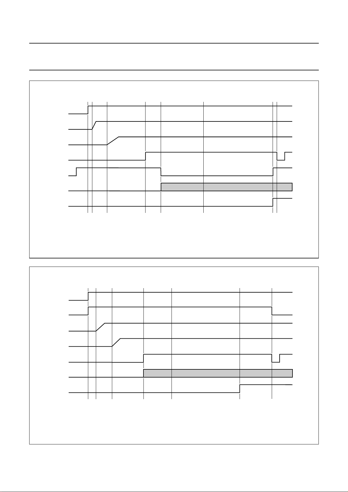
Activation sequence
When the card is inactive, pins VCC, CLK, RST and I/O are
LOW, having low impedance with respect to GND.
The step-up converter is stopped. The I/O is configured in
reception mode with a high impedance path to the
ISO 7816UART.Anyspurious pulses from the card during
power-up will have no effect until I/O is enabled. When
requirements are fulfilled (correct voltage supply, card
present, no hardware problems), the microcontroller may
initiate an activation sequence by setting bit CMDVCC
HIGH (t0).
• The step-up converter starts (t1)
• VCCstarts rising from 0 to 5 V or to 3 V with a controlled
rise time of typically 0.16 V/µs(t2)
• I/O, contacts C4 and C8 buffers are enabled (t3);
integrated pull-up resistors of 10 kΩ are connected to
V
CC
• CLK is sent to the card (t4)
• RST buffer is enabled (t5).
In order to allow a precise count of clock pulses during
ATR in manual mode, a defined time window (t3/t5) is
opened where the clock may be sent to the card using
RSTIN.Beyond this window, RSTIN does not respond to a
clock pulse, and only monitors the card’s RST contact.
In automatic mode (ATREN set HIGH), RST is monitored
by the TDA8006, RSTIN is inactive and CLK is output by
the TDA8006 at t3. RST is LOW. If the card has not
responded within the period of 40100 CLK pulses for
versions C2 and C3 (45000 for version C1), RST is set
HIGH for a maximum of 40100 CLK pulses for versions
C2 and C3 (45000 for version C1).
It is also possible to customize the activation sequence by
keepingCLK STOP LOW with RSTINLOWbeyond t5,and
then output CLK using the CLK configuration.
2000 Oct 30 23
The sequencer is clocked by1⁄64f
which gives a time
INT
interval Toftypically25 µs. Thus t1=0to1⁄64T,t2=t1+T,
t3=t1+ 4T, t4=t3to t5 and t5=t1+ 7T.
Page 24
Philips Semiconductors Product specification
Multiprotocol IC Card coupler TDA8006
handbook, full pagewidth
CMDVCC
VUP
V
CC
I/O
RSTIN
CLK
RST
handbook, full pagewidth
CMDVCC
ATREN
VUP
V
CC
I/O
CLK
t0t
t
1
2
t
t
3
4
t5 (= t
act
)
ATR
MGR235
Fig.11 Manual activation sequence using t3/t5.
RST
t0t
(1) CLK = 45000 for version C1 or 40100 for versions C2 and C3.
t
1
2
t
3
t5 (= t
Fig.12 Automatic activation sequence.
2000 Oct 30 24
act
)
ATRnote1
MGR236
Page 25
Philips Semiconductors Product specification
Multiprotocol IC Card coupler TDA8006
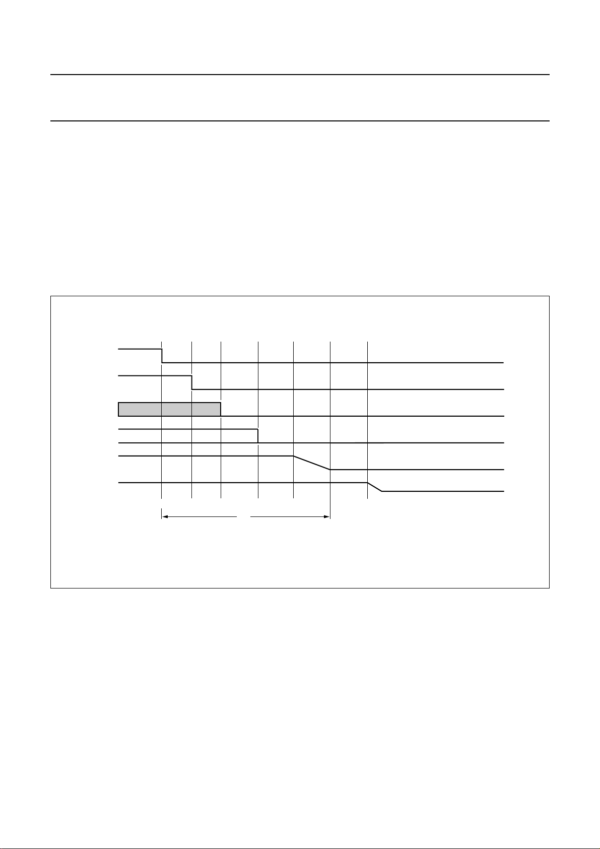
Deactivation sequence
When the session has completed, the microcontroller sets
CMDVCC LOW (t10). The circuit then executes an
automatic deactivation sequence:
• Card reset (RST goes LOW) (t11)
• Clock is stopped (t12)
• I/O goes LOW (t13)
• VCC falls to 0 V with typically 0.16 V/µs slew rate (t14)
• The step-up converter is stopped and CLK, RST, V
CC
and I/O become low impedance to GND (t15).
handbook, full pagewidth
CMDVCC
RST
CLK
t11=t10+1⁄64T, t12=t11+1⁄2T, t13=t11+T,
t14=t11+3⁄2T, t15=t11+ 5T.
tde is the time that VCC requires to fall to less than 0.3 V.
I/O
V
CC
VUP
t
t
10
t
11
12
t
13
t
de
Fig.13 Deactivation sequence.
Protection
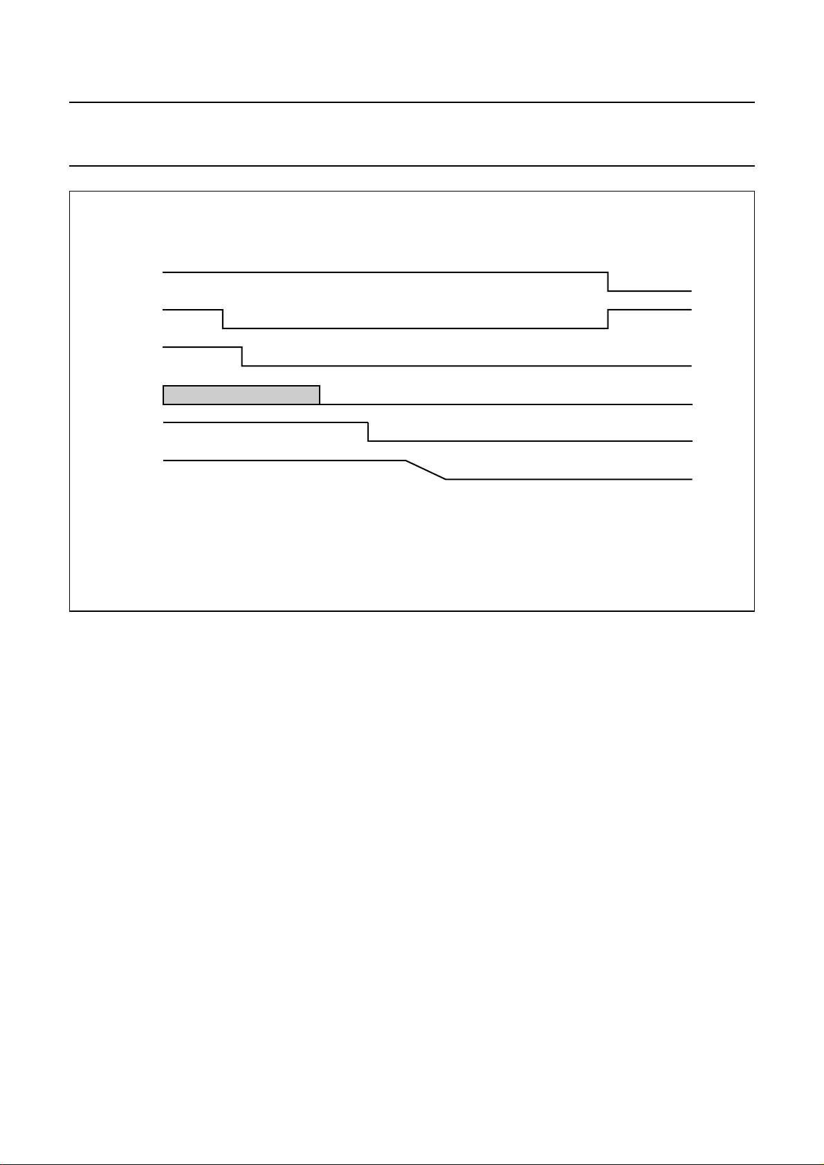
The main hardware fault conditions monitored by the
circuit are:
• Overcurrent on V
CC
• Short circuits between VCC and other contacts
• Card take-off during transaction.
Whenone of these problems is detected, the security logic
block sets the OFF bit LOW which generates an interrupt
warning the microcontroller and initiates an automatic
deactivation of the contacts.
t
14
t
15
MGR237
When the deactivation has completed and CMDVCC has
beensetLOW, the OFF bitgoesHIGH,unless the problem
was caused by a card extraction, in which case it remains
LOW until a card is inserted.
2000 Oct 30 25
Page 26
Philips Semiconductors Product specification
Multiprotocol IC Card coupler TDA8006
handbook, full pagewidth
CMDVCC
OFF
RST
CLK
I/O
V
CC
MGR238
Fig.14 Emergency deactivation sequence after VCC short circuited to ground.
Auxiliary contacts C4 and C8
The auxiliary contacts C4 and C8 are controlled by ports
P34 and P35 through two identical pseudo-bidirectional
I/O lines.
In the Idle state, port P34 is pulled HIGH to VDD by an
integrated 20 kΩ resistor and C4 is pulled HIGH to VCCby
an integrated 10 kΩ resistor. This allows operation with a
VCCvalue of 3 V and a VDDvalue of 5 V. The first side on
which a falling edge occurs becomes the master.
An anti-latch circuit disables the detection of a falling edge
on the other side, which becomes the slave.
After a delay of approximately 200 ns (td), the N transistor
on the slave side is turned on which transmits the ‘0’
present on the master side. When the master side goes
back to logic 1, the P transistor on the slave side is turned
on during td, and then both sides return to their idle states.
The maximum frequency on the I/O lines is 1 MHz.
2000 Oct 30 26
Page 27
Philips Semiconductors Product specification
Multiprotocol IC Card coupler TDA8006
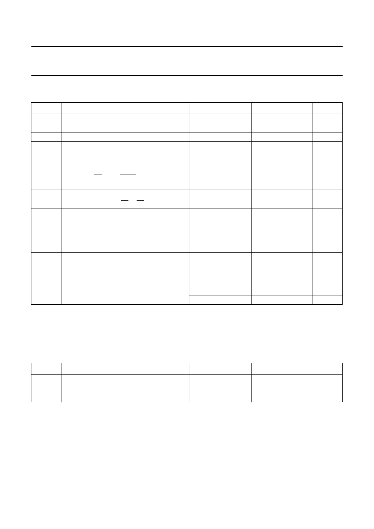
LIMITING VALUES
In accordance with the Absolute Maximum Rating System (IEC 134).
SYMBOL PARAMETER CONDITIONS MIN. MAX. UNIT
V
DDA
V
DDD
V
n1
V
n2
I
n1
I
n3
I
n6
I
n7
P
tot
T
stg
T
j
V
esd
analog supply voltage −0.5 +6.5 V
digital supply voltage −0.5 +6.5 V
all input voltages except S1, S2 and VUP −0.5 VDD+ 0.5 V
voltage on pins S1, S2 and VUP −0.5 +7.5 V
DC current into XTAL1, XTAL2, P30/RXD,
−5+5mA
P31/TXD, RESET, P33/INT1, P36/WR,
P37/RD, P00 to P07, P20 to P27, P10/T2,
P11/T2EX, EA, ALE, PSEN, CDELAY, PRES,
INHIB, CLKOUT and TEST
DC current from or to pins S1, S2 and VUP −200 +200 mA
DC current from or to K0 to K3 −5+5mA
DC current from or into pin ALARM
see Table 12 −5+5mA
(according to option choice)
total power dissipation T
= −20 to +85 °C
amb
QFP44 − 400 mW
QFP64 − 500 mW
storage temperature −55 +150 °C
junction temperature − 140 °C
electrostatic discharge on pins I/O, V
CC
−6+6kV
RST, CLK, C4, C8
and PRES
on other pins −2+2kV
HANDLING
Inputs and outputs are protected against electrostatic discharge in normal handling. However, to be totally safe, it is
desirable to take normal precautions appropriate to handling MOS devices.
THERMAL CHARACTERISTICS
SYMBOL PARAMETER CONDITIONS VALUE UNIT
R
th(j-a)
thermal resistance from junction to ambient in free air
QFP64 51 K/W
QFP44 64 K/W
2000 Oct 30 27
Page 28
Philips Semiconductors Product specification
Multiprotocol IC Card coupler TDA8006
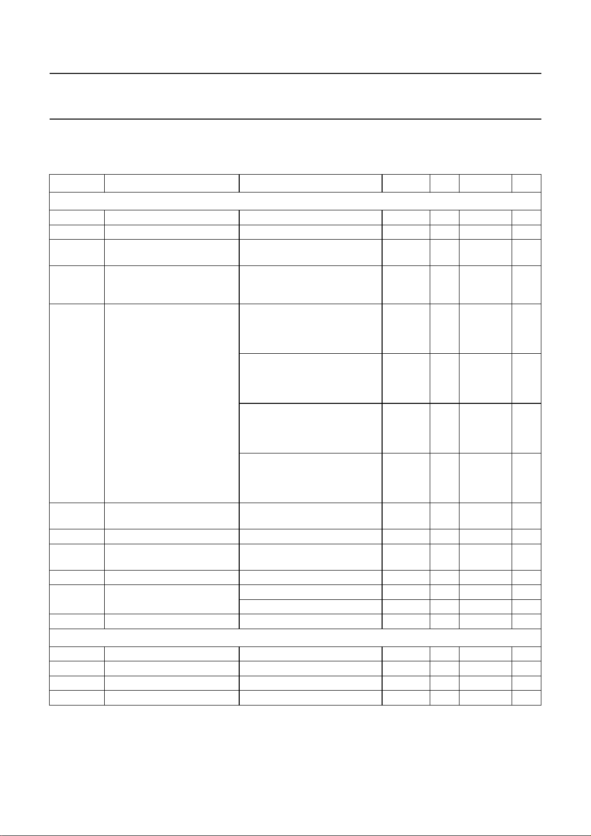
CHARACTERISTICS
VDD=5V; VSS=0V; T
specified.
SYMBOL PARAMETER CONDITIONS MIN. TYP. MAX. UNIT
Supply
V
DDA
V
DDD
I
DD(pd)
analog supply voltage 4.2 − 6.0 V
digital supply voltage 4.2 − 6.0 V
supply current in power-down
mode
I
DD(sm)
I
DD(om)
V
th(VDD)
supply current in sleep mode card powered, microcontroller in
supply current operating mode ICC= 65 mA; f
threshold voltage on V
(falling)
V
hys(VthVDD)
V
th(CDELAY)
hysteresis on V
threshold voltage on
pin CDELAY
V
CDELAY
I
CDELAY
t
W
voltage on pin CDELAY −−VDDV
output current at pin CDELAY pin grounded (charge) −−1−µA
ALARM pulse width C
ALARM (open drain active HIGH or LOW output)
I
OH
V
OL
I
OL
V
OH
HIGH-level output current active LOW option; VOH=5V −−10 µA
LOW-level output voltage active LOW option; IOL=2mA −0.3 − +0.4 V
LOW-level output current active HIGH option; VOL=0V −−−10 µA
HIGH-level output voltage active HIGH option; IOH= −2mA VDD− 0.8 − VDD+ 0.3 V
=25°C; for general purpose I/O ports refer to 80CE560 data sheet; unless otherwise
amb
VDD= 5 V; card inactive; note 1 −−250 µA
−−1500 µA
power-downmode but with clock
stopped; note 1
f
= 10 MHz; f
clk
f
CLKOUT
= 20 MHz;
xtal
= 20 MHz;
osc
= 20 MHz; 5 V card;
130 − 180 mA
notes 1 and 2
= 65 mA; f
I
CC
f
= 10 MHz; f
clk
f
CLKOUT
= 20 MHz; 3 V card;
= 20 MHz;
xtal
= 20 MHz;
osc
65 − 90 mA
notes 1 and 2
unloaded; f
f
= 5 MHz; f
clk
f
CLKOUT
= 20 MHz;
xtal
= 10 MHz;
osc
= 5 MHz; 5 V card;
1 − 6mA
notes 1 and 2
unloaded; f
f
= 5 MHz; f
clk
f
CLKOUT
= 20 MHz;
xtal
= 10 MHz;
osc
= 5 MHz; 3 V card;
0.5 − 4mA
notes 1 and 2
DD
th(VDD)
3.6 − 3.95 V
50 − 250 mV
− 1.38 − V
V
CDELAY=VDD
CDELAY
(discharge) − 2 − mA
=10nF − 10 − ms
2000 Oct 30 28
Page 29
Philips Semiconductors Product specification
Multiprotocol IC Card coupler TDA8006
SYMBOL PARAMETER CONDITIONS MIN. TYP. MAX. UNIT
Crystal oscillator
f
xtal
f
ext
CLKOUT
f
CLKOUT
V
OL
V
OH
t
o(r)
t
o(f)
δ duty factor C
Step-up converter
f
INT
V
VUP
Reset output to the card (pin RST)
V
o(RST)
I
o(RST)
V
OL
V
OH
t
r
t
f
Clock output to the card (pin CLK)
V
o(CLK)
I
o(CLK)
V
OL
V
OH
t
r
t
f
f
CLK
δ duty factor C
SR slew rate (rise and fall) C
crystal frequency 4 − 25 MHz
frequency of external signal
0 − 25 MHz
applied on pin XTAL1
frequency on pin CLKOUT 0 − 25 MHz
LOW-level output voltage IOL=5mA −−0.8 V
HIGH-level output voltage IOH= −5mA VDD− 1 −− V
output rise time CL=60pF −−10 ns
output fall time CL=60pF −−10 ns
=60pF 40 − 60 %
L
internal oscillation frequency 2 2.5 3 MHz
voltage on pin VUP − 6.5 − V
output voltage inactive mode; no load 0 − 0.1 V
inactive mode; I
= 1 mA 0 − 0.3 V
o(RST)
output current when inactive and pin grounded 0 −−1mA
LOW-level output voltage IOL= 200 µA0−0.3 V
HIGH-level output voltage IOH= −200 µAV
− 0.7 − V
CC
CC
V
rise time CL=30pF −−0.1 µs
fall time CL=30pF −−0.1 µs
output voltage inactive mode; no load 0 − 0.1 V
inactive mode; I
= 1 mA 0 − 0.3 V
o(CLK)
output current when inactive and pin grounded 0 −−1mA
LOW-level output voltage IOL= 200 µA0−0.3 V
HIGH-level output voltage IOH= −200 µAV
− 0.5 − V
CC
CC
V
rise time CL=30pF −−8ns
fall time CL=30pF −−8ns
clock frequency 1.25 MHz idle configuration 1 1.25 1.5 MHz
operational 0 − 10 MHz
=30pF 45 − 55 %
L
=30pF 0.2 −− V/ns
L
2000 Oct 30 29
Page 30
Philips Semiconductors Product specification
Multiprotocol IC Card coupler TDA8006
SYMBOL PARAMETER CONDITIONS MIN. TYP. MAX. UNIT
Card supply voltage (pin VCC); note 3
V
O(VCC)
card supply output voltage inactive
no load 0 − 0.1 V
I
O(VCC)
pin grounded 0 −−1mA
active
I
< 65 mA; 5 V card 4.75 5 5.25 V
CC
I
< 65 mA; 3 V card 2.8 3 3.2 V
CC
current pulses of 40 nAs with
I
< 200 mA; t < 400 ns;
CC
f < 20 MHz; 5 V card
current pulses of 24 nAs with
I
< 200 mA; t < 400 ns;
CC
f < 20 MHz; 3 V card
I
O(VCC)
I
CC(sd)
card supply output current from 0 to 3 or 5 V −−65 mA
short circuited to GND −−250 mA
V
CC
shutdown current at pin V
CC
SR slew rate up or down
(capacitor = 100 to 300 nF)
Data line (pin I/O); note 4
V
o(I/O)
output voltage inactive
no load 0 − 0.1 V
I
=1mA −−0.3 V
o(I/O)
I
o(I/O)
V
OL
output current inactive and pin grounded 0 −−1mA
LOW-level output voltage I/O configured as output;
IOL=1mA
V
OH
HIGH-level output voltage I/O configured as output;
IOH< −50 µA
V
IL
V
IH
I
IL
I
LIH
LOW-level input voltage I/O configured as input −0.3 − +0.8 V
HIGH-level input voltage I/O configured as input 1.5 − V
LOW-level input current VIL=0 V −−−600 µA
HIGH-level input leakage
VIH=V
CC
current
t
i(r)
t
i(f)
t
o(r)
t
o(f)
R
pu(int)
input rise time CL=30pF −−1 µs
input fall time CL=30pF −−1 µs
output rise time CL=30pF −−0.1 µs
output fall time CL=30pF −−0.1 µs
internal pull-up resistance
between I/O and V
CC
=1mA 0 − 0.3 V
4.6 − 5.4 V
2.75 − 3.25 V
−−80 − mA
0.10 0.16 0.30 V/µs
0 − 0.3 V
0.8V
CC
− VCC+ 0.25 V
CC
−−20 µA
81013kΩ
V
2000 Oct 30 30
Page 31
Philips Semiconductors Product specification
Multiprotocol IC Card coupler TDA8006
SYMBOL PARAMETER CONDITIONS MIN. TYP. MAX. UNIT
Auxiliary card contacts (C4 and C8); note 5
V
o(C4,C8)
I
o(C4,C8)
V
OL
V
OH
V
IL
V
IH
I
IL
I
LIH
t
i(r)
t
i(f)
t
o(r)
t
o(f)
t
d
R
pu(int)
f
(max)
Timing
t
act
t
de
t
3(start)
t
5(end)
Output ports from extension (K0 to K3)
V
OL
V
OH
output voltage inactive
no load 0 − 0.1 V
I
o(C4,C8)
=1mA −−0.3 V
output current inactive and pin grounded −−−1mA
LOW-level output voltage C4 or C8 configured as output;
0 − 0.3 V
IOL=1mA
HIGH-level output voltage C4 or C8 and I/O configured as
0.8V
CC
− VCC+ 0.25 V
output; IOH< −50 µA
LOW-level input voltage C4 or C8 configured as input −0.3 − +0.8 V
HIGH-level input voltage C4 or C8 configured as input 1.5 − V
CC
V
LOW-level input current VIL=0V −−−600 µA
HIGH-level input leakage
VIH=V
CC
−−20 µA
current
input rise time CL=30pF −−1 µs
input fall time CL=30pF −−1 µs
output rise time CL=30pF −−0.1 µs
output fall time CL=30pF −−0.1 µs
delay between falling edge on
−−200 ns
P34 and C4 (or C4 and P34)
internal pull-up resistance
81013kΩ
between C4 and VCC and
C8 and V
maximum frequency on
CC
−−1 MHz
C4 or C8
activation sequence duration −−225 µs
deactivation sequence
−−100 µs
duration
start of the window for sending
−−130 µs
clock to the card
end of the window for sending
145 −− µs
clock to the card
LOW-level output voltage IOL=2mA −−0.4 V
HIGH-level output voltage IOH= −2mA VDD− 1 −− V
2000 Oct 30 31
Page 32
Philips Semiconductors Product specification
Multiprotocol IC Card coupler TDA8006
SYMBOL PARAMETER CONDITIONS MIN. TYP. MAX. UNIT
Card presence input (pin PRES)
V
IL
V
IH
I
LIL
LOW-level input voltage −−0.3V
HIGH-level input voltage 0.7V
LOW-level input leakage
Vi=0V −−20 µA
DD
−− V
DD
current
I
LIH
HIGH-level input leakage
Vi=V
DD
−−20 µA
current
Notes
1. IDD in all configurations include the current at pins VDD, V
DDA
and V
DDRAM
.
2. Values given for program executed from internal ROM. Current consumption may be higher if program is executed
from external ROM or if charges are present on I/O ports.
3. A ceramic multilayer capacitor having a minimum value of 100 nF with a low ESR should be used to obtain these
specifications.
4. The I/O line has an integrated 10 kΩ pull-up resistor at pin VCC.
5. Pins C4 and C8 have integrated 10 kΩ pull-up resistors at pin VCC; ports P34 and P35 have integrated 20 kΩ pull-up
resistors at pin VDD.
V
OPTIONS Table 12 Options
FEATURES OPTIONS
Alarm active HIGH active LOW
Presence active HIGH active LOW
MOVEC protection on off
2000 Oct 30 32
Page 33
This text is here in white to force landscape pages to be rotated correctly when browsing through the pdf in the Acrobat reader.This text is here in
_white to force landscape pages to be rotated correctly when browsing through the pdf in the Acrobat reader.This text is here inThis text is here in
white to force landscape pages to be rotated correctly when browsing through the pdf in the Acrobat reader. white to force landscape pages to be ...
2000 Oct 30 33
handbook, full pagewidth
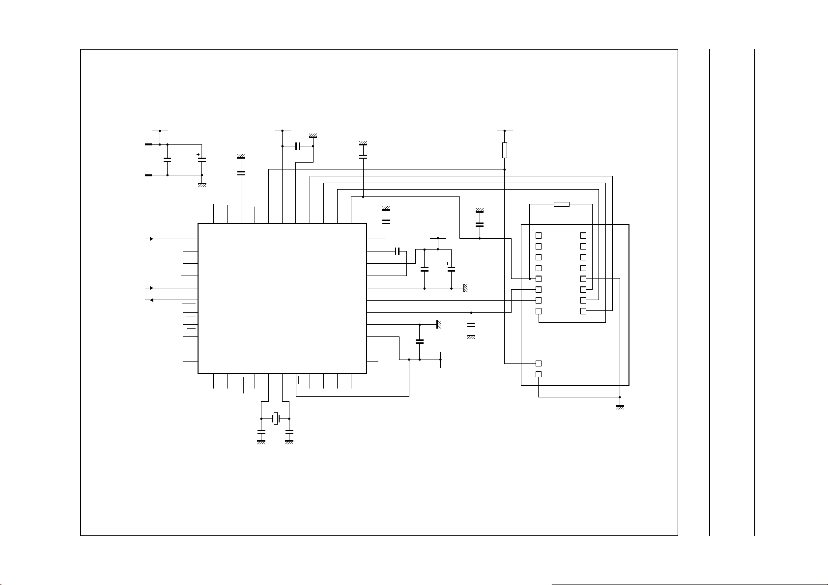
APPLICATION INFORMATION
Philips Semiconductors Product specification
Multiprotocol IC Card coupler TDA8006
+5 V
GND
reset
RX
TX
V
DD
2
J1
C20
100 nF
1
J1
RESET
P10/T2
P11/T2EX
P30/RXD
P31/TXD
P33/INT1
P36/WR
P37/RD
C21
33 µF
TEST
ALARM
33 32 31 30 29 28 27 26 25 24 23
34
35
36
n.c.
37
38
39
40
41
42
P20
43
P21
44
1
3
P222P23
C21
33 pF
C7
4.7
nF
CDELAY
CLKOUT
TDA8006AH
4
5
ALE
PSEN
V
DD
C9
100 nF
PRES
VDDGNDC8C4
6
7EA8
XTAL1
XTAL2
14.745 MHz
Y2
C20
33 pF
10
P039P02
I/O
11
P01
V
22
21
20
19
18
17
16
15
14
13
12
P00
CC
C14
100 nF
VUP
100 nF
S2
V
DDA
S1
AGND
CLK
RST
GNDRAM
V
DDRAM
n.c.
n.c.
C5
100 nF
C1
V
DD
C2
100
nF
C6
100 nF
V
DD
C3
10 µF
C4
100
nF
C10
47 pF
V
DD
R2
100 kΩ
R1
0 Ω
C8
C4
C7
C3
C6
C2
C5
C1
C1I
C5I
C2I
C6I
C3I
C7I
C4I
C8I
CARD READ UNIT
K1
K2
MGR239
Fig.15 Application diagram.
Page 34
Philips Semiconductors Product specification
Multiprotocol IC Card coupler TDA8006
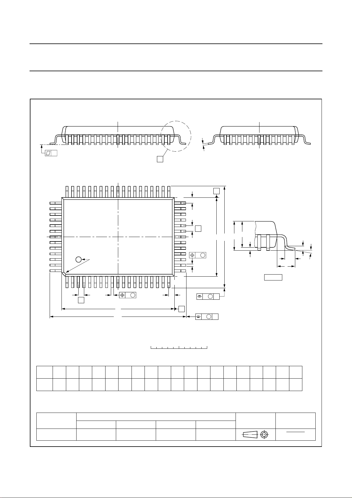
PACKAGE OUTLINES
QFP64: plastic quad flat package; 64 leads (lead length 1.95 mm); body 14 x 20 x 2.8 mm
c
y
X
SOT319-2
51 33
52
pin 1 index
64
1
b
e
p
D
H
D
DIMENSIONS (mm are the original dimensions)
mm
A
max.
3.20
0.25
0.05
2.90
2.65
0.25
cE
p
0.50
0.25
0.35
0.14
UNIT A1A2A3b
A
32
Z
E
e
A
H
E
E
2
A
w M
b
p
20
19
w M
Z
D
v M
A
B
v M
B
0 5 10 mm
scale
(1)
(1) (1)(1)
D
20.1
19.9
eH
H
14.1
13.9
24.2
1
23.6
D
E
18.2
17.6
LL
p
1.0
0.6
0.2 0.10.21.95
(A )
A
1
3
θ
L
p
L
detail X
Zywv θ
Z
E
D
1.2
0.8
o
7
o
0
1.2
0.8
Note
1. Plastic or metal protrusions of 0.25 mm maximum per side are not included.
OUTLINE
VERSION
IEC JEDEC EIAJ
REFERENCES
SOT319-2 MO-112
2000 Oct 30 34
EUROPEAN
PROJECTION
ISSUE DATE
97-08-01
99-12-27
Page 35
Philips Semiconductors Product specification
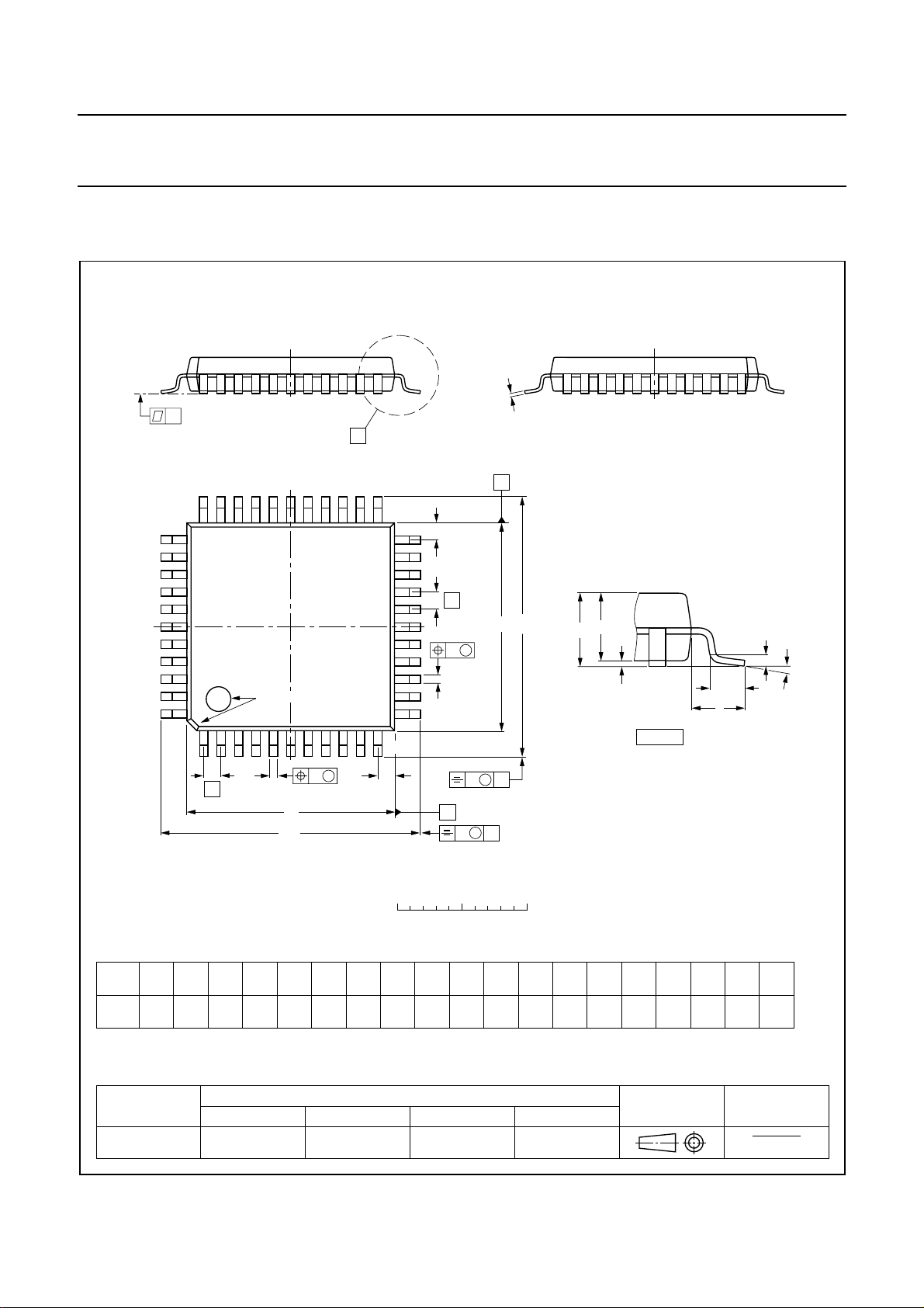
Multiprotocol IC Card coupler TDA8006
QFP44: plastic quad flat package; 44 leads (lead length 1.3 mm); body 10 x 10 x 1.75 mm
c
y
X
A
33 23
34
pin 1 index
44
1
22
Z
E
e
H
E
E
w M
b
p
12
11
A
2
A
A
1
detail X
SOT307-2
(A )
3
θ
L
p
L
w M
b
e
p
D
H
D
Z
D
B
0 2.5 5 mm
scale
DIMENSIONS (mm are the original dimensions)
mm
A
max.
2.10
0.25
0.05
1.85
1.65
0.25
UNIT A1A2A3b
cE
p
0.40
0.25
0.20
0.14
(1)
(1) (1)(1)
D
10.1
9.9
eH
10.1
9.9
12.9
0.8 1.3
12.3
Note
1. Plastic or metal protrusions of 0.25 mm maximum per side are not included.
OUTLINE
VERSION
IEC JEDEC EIAJ
REFERENCES
SOT307-2
2000 Oct 30 35
v M
H
v M
D
A
B
E
12.9
12.3
LL
p
0.95
0.55
0.15 0.10.15
EUROPEAN
PROJECTION
Z
D
1.2
0.8
Zywv θ
E
o
1.2
10
o
0.8
0
ISSUE DATE
95-02-04
97-08-01
Page 36

Philips Semiconductors Product specification
Multiprotocol IC Card coupler TDA8006
SOLDERING
Introduction to soldering surface mount packages
Thistextgivesa very brief insight to acomplextechnology.
A more in-depth account of soldering ICs can be found in
our
“Data Handbook IC26; Integrated Circuit Packages”
(document order number 9398 652 90011).
There is no soldering method that is ideal for all surface
mount IC packages. Wave soldering is not always suitable
for surface mount ICs, or for printed-circuit boards with
high population densities. In these situations reflow
soldering is often used.
Reflow soldering
Reflow soldering requires solder paste (a suspension of
fine solder particles, flux and binding agent) to be applied
totheprinted-circuitboardbyscreenprinting,stencilling or
pressure-syringe dispensing before package placement.
Several methods exist for reflowing; for example,
infrared/convection heating in a conveyor type oven.
Throughput times (preheating, soldering and cooling) vary
between 100 and 200 seconds depending on heating
method.
Typical reflow peak temperatures range from
215 to 250 °C. The top-surface temperature of the
packages should preferable be kept below 230 °C.
• Use a double-wave soldering method comprising a
turbulent wave with high upward pressure followed by a
smooth laminar wave.
• For packages with leads on two sides and a pitch (e):
– larger than or equal to 1.27 mm, the footprint
longitudinal axis is preferred to be parallel to the
transport direction of the printed-circuit board;
– smaller than 1.27 mm, the footprint longitudinal axis
must be parallel to the transport direction of the
printed-circuit board.
The footprint must incorporate solder thieves at the
downstream end.
• Forpackageswith leads on four sides,thefootprintmust
be placed at a 45° angle to the transport direction of the
printed-circuit board. The footprint must incorporate
solder thieves downstream and at the side corners.
During placement and before soldering, the package must
be fixed with a droplet of adhesive. The adhesive can be
applied by screen printing, pin transfer or syringe
dispensing. The package can be soldered after the
adhesive is cured.
Typical dwell time is 4 seconds at 250 °C.
A mildly-activated flux will eliminate the need for removal
of corrosive residues in most applications.
Manual soldering
Wave soldering
Conventional single wave soldering is not recommended
forsurfacemount devices (SMDs) or printed-circuit boards
with a high component density, as solder bridging and
non-wetting can present major problems.
To overcome these problems the double-wave soldering
method was specifically developed.
If wave soldering is used the following conditions must be
observed for optimal results:
Fix the component by first soldering two
diagonally-opposite end leads. Use a low voltage (24 V or
less) soldering iron applied to the flat part of the lead.
Contact time must be limited to 10 seconds at up to
300 °C.
When using a dedicated tool, all other leads can be
soldered in one operation within 2 to 5 seconds between
270 and 320 °C.
2000 Oct 30 36
Page 37

Philips Semiconductors Product specification
Multiprotocol IC Card coupler TDA8006
Suitability of surface mount IC packages for wave and reflow soldering methods
PACKAGE
WAVE REFLOW
(1)
BGA, LFBGA, SQFP, TFBGA not suitable suitable
SOLDERING METHOD
HBCC, HLQFP, HSQFP, HSOP, HTQFP, HTSSOP, SMS not suitable
(3)
PLCC
, SO, SOJ suitable suitable
LQFP, QFP, TQFP not recommended
SSOP, TSSOP, VSO not recommended
(2)
(3)(4)
(5)
suitable
suitable
suitable
Notes
1. All surface mount (SMD) packages are moisture sensitive. Depending upon the moisture content, the maximum
temperature (with respect to time) and body size of the package, there is a risk that internal or external package
cracks may occur due to vaporization of the moisture in them (the so called popcorn effect). For details, refer to the
Drypack information in the
“Data Handbook IC26; Integrated Circuit Packages; Section: Packing Methods”
.
2. These packages are not suitable for wave soldering as a solder joint between the printed-circuit board and heatsink
(at bottom version) can not be achieved, and as solder may stick to the heatsink (on top version).
3. If wave soldering is considered, then the package must be placed at a 45° angle to the solder wave direction.
The package footprint must incorporate solder thieves downstream and at the side corners.
4. Wave soldering is only suitable for LQFP, TQFP and QFP packages with a pitch (e) equal to or larger than 0.8 mm;
it is definitely not suitable for packages with a pitch (e) equal to or smaller than 0.65 mm.
5. Wave soldering is only suitable for SSOP and TSSOP packages with a pitch (e) equal to or larger than 0.65 mm; it is
definitely not suitable for packages with a pitch (e) equal to or smaller than 0.5 mm.
2000 Oct 30 37
Page 38

Philips Semiconductors Product specification
Multiprotocol IC Card coupler TDA8006
DATA SHEET STATUS
DATA SHEET STATUS
Objective specification Development This data sheet contains the design target or goal specifications for
Preliminary specification Qualification This data sheet contains preliminarydata, and supplementary data will be
Product specification Production This data sheet contains final specifications. Philips Semiconductors
Note
1. Please consult the most recently issued data sheet before initiating or completing a design.
DEFINITIONS
Short-form specification The data in a short-form
specification is extracted from a full data sheet with the
same type number and title. For detailed information see
the relevant data sheet or data handbook.
Limiting values definition Limiting values given are in
accordance with the Absolute Maximum Rating System
(IEC 60134). Stress above one or more of the limiting
values may cause permanent damage to the device.
These are stress ratings only and operation of the device
attheseorat any other conditions above those given inthe
Characteristics sections of the specification is not implied.
Exposure to limiting values for extended periods may
affect device reliability.
Application information Applications that are
described herein for any of these products are for
illustrative purposes only. Philips Semiconductors make
norepresentationor warranty that suchapplicationswillbe
suitable for the specified use without further testing or
modification.
PRODUCT
STATUS
DEFINITIONS
product development. Specification may change in any manner without
notice.
published at a later date. Philips Semiconductors reserves the right to
make changes at any time without notice in order to improve design and
supply the best possible product.
reserves the right to make changes at any time without notice in order to
improve design and supply the best possible product.
DISCLAIMERS
Life support applications These products are not
designed for use in life support appliances, devices, or
systems where malfunction of these products can
reasonably be expected to result in personal injury. Philips
Semiconductorscustomersusing or selling theseproducts
for use in such applications do so at their own risk and
agree to fully indemnify Philips Semiconductors for any
damages resulting from such application.
Right to make changes Philips Semiconductors
reserves the right to make changes, without notice, in the
products, including circuits, standard cells, and/or
software, described or contained herein in order to
improve design and/or performance. Philips
Semiconductors assumes no responsibility or liability for
theuseof any of these products,conveysnolicenceor title
under any patent, copyright, or mask work right to these
products,andmakesnorepresentations or warranties that
these products are free from patent, copyright, or mask
work right infringement, unless otherwise specified.
(1)
2000 Oct 30 38
Page 39

Philips Semiconductors Product specification
Multiprotocol IC Card coupler TDA8006
NOTES
2000 Oct 30 39
Page 40

Philips Semiconductors – a w orldwide compan y
Argentina: see South America
Australia: 3 Figtree Drive, HOMEBUSH, NSW 2140,
Tel. +61 2 9704 8141, Fax. +61 2 9704 8139
Austria: Computerstr. 6, A-1101 WIEN, P.O. Box 213,
Tel. +43 1 60 101 1248, Fax. +43 1 60 101 1210
Belarus: Hotel Minsk Business Center, Bld. 3, r. 1211, Volodarski Str. 6,
220050 MINSK, Tel. +375 172 20 0733, Fax. +375 172 20 0773
Belgium: see The Netherlands
Brazil: see South America
Bulgaria: Philips Bulgaria Ltd., Energoproject, 15th floor,
51 James Bourchier Blvd., 1407 SOFIA,
Tel. +359 2 68 9211, Fax. +359 2 68 9102
Canada: PHILIPS SEMICONDUCTORS/COMPONENTS,
Tel. +1 800 234 7381, Fax. +1 800 943 0087
China/Hong Kong: 501 Hong Kong Industrial Technology Centre,
72 Tat Chee Avenue, Kowloon Tong, HONG KONG,
Tel. +852 2319 7888, Fax. +852 2319 7700
Colombia: see South America
Czech Republic: see Austria
Denmark: Sydhavnsgade 23, 1780 COPENHAGEN V,
Tel. +45 33 29 3333, Fax. +45 33 29 3905
Finland: Sinikalliontie 3, FIN-02630 ESPOO,
Tel. +358 9 615 800, Fax. +358 9 6158 0920
France: 51 Rue Carnot, BP317, 92156 SURESNES Cedex,
Tel. +33 1 4099 6161, Fax. +33 1 4099 6427
Germany: Hammerbrookstraße 69, D-20097 HAMBURG,
Tel. +49 40 2353 60, Fax. +49 40 2353 6300
Hungary: see Austria
India: Philips INDIA Ltd, Band Box Building, 2nd floor,
254-D, Dr. Annie Besant Road, Worli, MUMBAI 400 025,
Tel. +91 22 493 8541, Fax. +91 22 493 0966
Indonesia: PT PhilipsDevelopment Corporation, Semiconductors Division,
Gedung Philips, Jl. Buncit Raya Kav.99-100, JAKARTA 12510,
Tel. +62 21 794 0040 ext. 2501, Fax. +62 21 794 0080
Ireland: Newstead, Clonskeagh, DUBLIN 14,
Tel. +353 1 7640 000, Fax. +353 1 7640 200
Israel: RAPAC Electronics, 7 Kehilat Saloniki St, PO Box 18053,
TEL AVIV 61180, Tel. +972 3 645 0444, Fax. +972 3 649 1007
Italy: PHILIPS SEMICONDUCTORS, Via Casati, 23 - 20052 MONZA (MI),
Tel. +39 039 203 6838, Fax +39 039 203 6800
Japan: Philips Bldg 13-37, Kohnan 2-chome, Minato-ku,
TOKYO 108-8507, Tel. +81 3 3740 5130, Fax. +81 3 3740 5057
Korea: Philips House, 260-199 Itaewon-dong, Yongsan-ku, SEOUL,
Tel. +82 2 709 1412, Fax. +82 2 709 1415
Malaysia: No. 76 Jalan Universiti, 46200 PETALING JAYA, SELANGOR,
Tel. +60 3 750 5214, Fax. +60 3 757 4880
Mexico: 5900 Gateway East, Suite 200, EL PASO, TEXAS 79905,
Tel. +9-5 800 234 7381, Fax +9-5 800 943 0087
Middle East: see Italy
Netherlands: Postbus 90050, 5600 PB EINDHOVEN, Bldg. VB,
Tel. +31 40 27 82785, Fax. +31 40 27 88399
New Zealand: 2 Wagener Place, C.P.O. Box 1041, AUCKLAND,
Tel. +64 9 849 4160, Fax. +64 9 849 7811
Norway: Box 1, Manglerud 0612, OSLO,
Tel. +47 22 74 8000, Fax. +47 22 74 8341
Pakistan: see Singapore
Philippines: Philips Semiconductors Philippines Inc.,
106 Valero St. Salcedo Village, P.O. Box 2108 MCC, MAKATI,
Metro MANILA, Tel. +63 2 816 6380, Fax. +63 2 817 3474
Poland: Al.Jerozolimskie 195 B, 02-222 WARSAW,
Tel. +48 22 5710 000, Fax. +48 22 5710 001
Portugal: see Spain
Romania: see Italy
Russia: Philips Russia, Ul. Usatcheva 35A, 119048 MOSCOW,
Tel. +7 095 755 6918, Fax. +7 095 755 6919
Singapore: Lorong 1, Toa Payoh, SINGAPORE 319762,
Tel. +65 350 2538, Fax. +65 251 6500
Slovakia: see Austria
Slovenia: see Italy
South Africa: S.A. PHILIPS Pty Ltd., 195-215 Main Road Martindale,
2092 JOHANNESBURG, P.O. Box 58088 Newville 2114,
Tel. +27 11 471 5401, Fax. +27 11 471 5398
South America: Al. Vicente Pinzon, 173, 6th floor,
04547-130 SÃO PAULO, SP, Brazil,
Tel. +55 11 821 2333, Fax. +55 11 821 2382
Spain: Balmes 22, 08007 BARCELONA,
Tel. +34 93 301 6312, Fax. +34 93 301 4107
Sweden: Kottbygatan 7, Akalla, S-16485 STOCKHOLM,
Tel. +46 8 5985 2000, Fax. +46 8 5985 2745
Switzerland: Allmendstrasse 140, CH-8027 ZÜRICH,
Tel. +41 1 488 2741 Fax. +41 1 488 3263
Taiwan: Philips Semiconductors, 5F, No. 96, Chien Kuo N. Rd., Sec. 1,
TAIPEI, Taiwan Tel. +886 2 2134 2451, Fax. +886 2 2134 2874
Thailand: PHILIPS ELECTRONICS (THAILAND) Ltd.,
60/14 MOO 11, Bangna Trad Road KM. 3, Bagna, BANGKOK 10260,
Tel. +66 2 361 7910, Fax. +66 2 398 3447
Turkey: Yukari Dudullu, Org. San. Blg., 2.Cad. Nr. 28 81260 Umraniye,
ISTANBUL, Tel. +90 216 522 1500, Fax. +90 216 522 1813
Ukraine: PHILIPS UKRAINE, 4 Patrice Lumumba str., Building B, Floor 7,
252042 KIEV, Tel. +380 44 264 2776, Fax. +380 44 268 0461
United Kingdom: Philips Semiconductors Ltd., 276 Bath Road, Hayes,
MIDDLESEX UB3 5BX, Tel. +44 208 730 5000, Fax. +44 208 754 8421
United States: 811 East Arques Avenue, SUNNYVALE, CA 94088-3409,
Tel. +1 800 234 7381, Fax. +1 800 943 0087
Uruguay: see South America
Vietnam: see Singapore
Yugoslavia: PHILIPS, Trg N. Pasica 5/v, 11000 BEOGRAD,
Tel. +381 11 3341 299, Fax.+381 11 3342 553
For all other countries apply to: Philips Semiconductors,
Marketing Communications, Building BE-p, P.O. Box 218, 5600 MD EINDHOVEN,
The Netherlands, Fax. +31 40 27 24825
© Philips Electronics N.V. SCA
All rights are reserved. Reproduction in whole or in part is prohibited without the prior written consent of the copyright owner.
The information presented in this document does not form part of any quotation or contract, is believed to be accurate and reliable and may be changed
without notice. No liability will be accepted by the publisher for any consequence of its use. Publication thereof does not convey nor imply any license
under patent- or other industrial or intellectual property rights.
2000
Internet: http://www.semiconductors.philips.com
70
Printed in The Netherlands 753504/04/pp40 Date of release:2000 Oct 30 Document order number: 9397 750 07622
 Loading...