

Page 1

INTEGRATED CIRCUITS
DATA SH EET
TDA8005
Low-power smart card coupler
Product specification
Supersedes data of 1995 Apr 13
File under Integrated Circuits, IC17
1996 Sep 25
Page 2

Philips Semiconductors Product specification
Low-power smart card coupler TDA8005
FEATURES
• VCC generation (5 V ±5%, 20 mA maximum with
controlled rise and fall times)
• Clock generation (up to 8 MHz), with two times
synchronous frequency doubling
• Clock STOP HIGH, clock STOP LOW or 1.25 MHz (from
internal oscillator) for cards power-down mode
• Specific UART on I/O for automatic direct/inverse
convention settings and error management at
character level
• Automatic activation and deactivation sequences
through an independent sequencer
• Supports the protocol T = 0 in accordance with
ISO 7816, GSM11.11 requirements (Global System for
Mobile communication); and EMV banking specification
approved for Final GSM11.11 Test Approval (FTA)
• Several analog options are available for different
applications (doubler or tripler DC/DC converter, card
presence, active HIGH or LOW, threshold voltage
supervisor, etc.
• Overloads and take-off protections
• Current limitations in the event of short-circuit
• Special circuitry for killing spikes during power-on or off
• Supply supervisor
• Step-up converter (supply voltage from 2.5 to 6 V)
• Power-down and sleep mode for low-power
consumption
• Enhanced ESD protections on card side
(6 kV minimum)
• Control and communication through a standard RS232
full duplex interface
• Optional additional I/O ports for:
– keyboard
– LEDs
– display
– etc.
• 80CL51 microcontroller core with 4 kbytes ROM and
256-byte RAM.
APPLICATIONS
• Portable smart card readers for protocol T = 0
• GSM mobile phones.
GENERAL DESCRIPTION
The TDA8005 is a low cost card interface for portable
smart card readers. Controlled through a standard serial
interface, it takes care of all ISO 7816 and GSM11-11
requirements. It gives the card and the set a very high level
of security, due to its special hardware against ESD,
short-circuiting, power failure, etc. Its integrated step-up
converter allows operation within a supply voltage range of
2.5 to 6 V.
The very low-power consumption in Power-down and
sleep modes saves battery power. A special version where
the internal connections to the controller are fed outside
through pins allows easy development and evaluation,
together with a standard 80CL51 microcontroller.
Development tools, application report and support
(hardware and software) are available.
The device can be supplied either as a masked chip with
standard software handling all communication between
smart card and a master controller in order to make the
application easier, or as a maskable device.
1996 Sep 25 2
Page 3

Philips Semiconductors Product specification
Low-power smart card coupler TDA8005
QUICK REFERENCE DATA
SYMBOL PARAMETER CONDITIONS MIN. TYP. MAX. UNIT
V
DD
I
DD(pd)
I
DD(sm)
I
DD(sm)
I
DD(om)
V
CC
I
CC
SR slew rate on V
t
de
t
act
f
xtal
T
amb
supply voltage doubler and tripler option 2.5 − 6.0 V
supply current in power-down mode VDD= 5 V; card inactive −−100 µA
supply current in sleep mode doubler card powered but clock
−−500 µA
stopped
supply current in sleep mode tripler card powered but clock
−−500 µA
stopped
supply current in operating mode unloaded; f
= 6.5 MHz;
f
µC
f
= 3.25 MHz
card
= 13 MHz;
xtal
card supply voltage including static and
−−5.5 mA
4.75 5.0 5.25 V
dynamic loads on 100 nF
capacitor
card supply current operating −−20 mA
limitation −−30 mA
(rise and fall) maximum load capacitor
CC
0.05 0.1 0.15 V/µs
150 nF (including typical
100 nF decoupling)
deactivation cycle duration −−100 µs
activation cycle duration −−100 µs
crystal frequency 2 − 16 MHz
operating ambient temperature −25 − +85 °C
ORDERING INFORMATION
TYPE
NUMBER
NAME DESCRIPTION VERSION
PACKAGE
TDA8005G LQFP64 plastic low profile quad flat package; 64 leads; body 10 × 10 × 1.4 mm SOT314-2
TDA8005H QFP44 plastic quad flat package; 44 leads (lead length 1.3 mm);
SOT307-2
body 10 × 10 × 1.75 mm
1996 Sep 25 3
Page 4
Philips Semiconductors Product specification
Low-power smart card coupler TDA8005
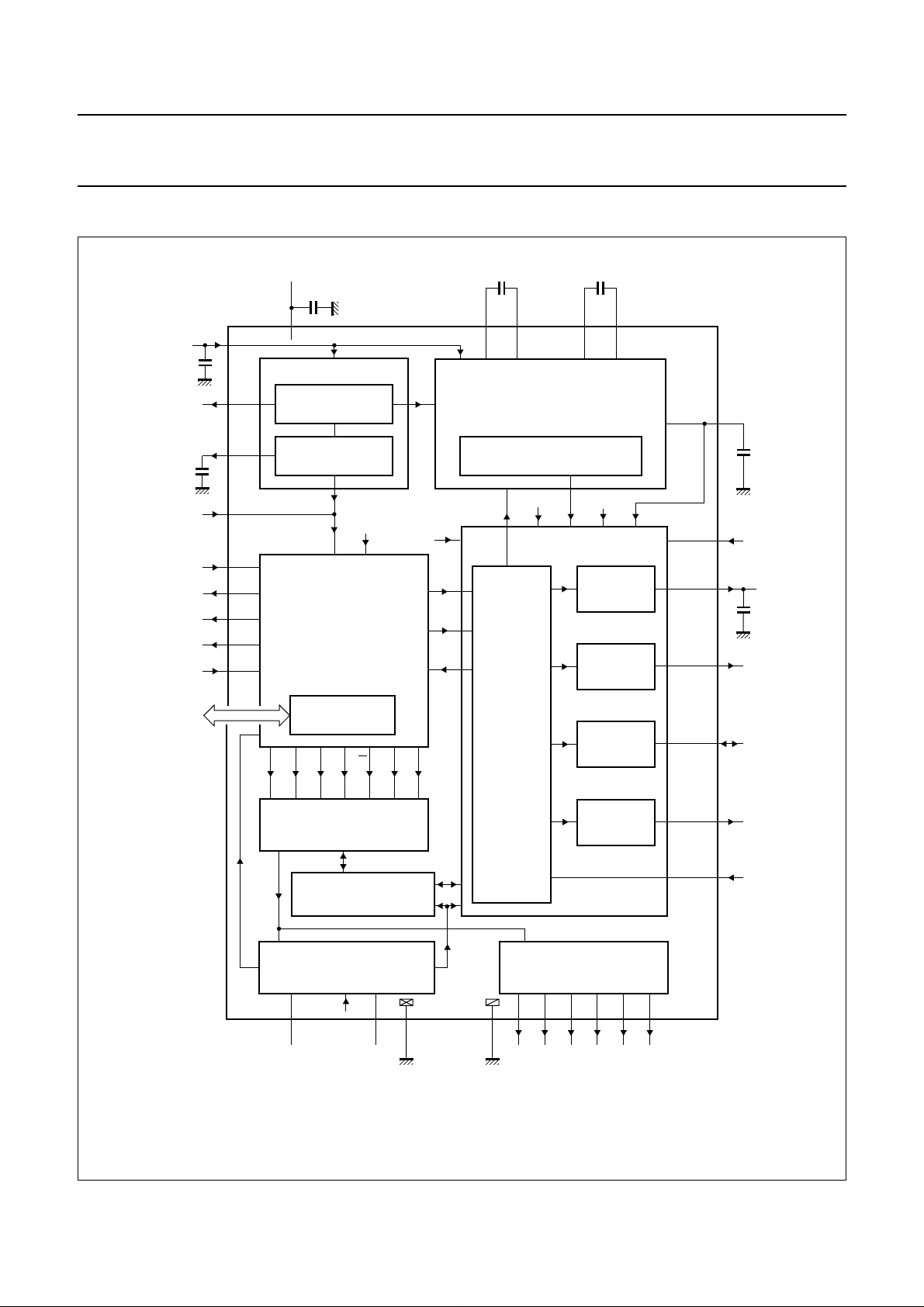
BLOCK DIAGRAM
V
handbook, full pagewidth
V
DDA
2.5 to 6 V
100 nF
ALARM
DELAY
DDD
100 nF
63
44
46
10
SUPPLY
INTERNAL
REFERENCE
VOLTAGE SENSE
2.3 to 2.7 V
ref
47 nF
S1 S2
64 61 3 62
STEP-UP CONVERTER
INTERNAL OSCILLATOR
2.5 MHz
47 nF
S3 S4
V
60
UP S5
47 nF
RESET
RxD
TxD
AUX1
AUX2
INT1
P00
P37
22
28
29
32
33
30
(1)
to
data clk EN S0 S1 R/W
µCclk
alarm
V
CONTROLLER
CL51
4 kbytes ROM
256-byte RAM
OPTIONAL
PORTS
PERIPHERAL
INTERFACE
ISO 7816 UART
TDA8005G
DDD
skill
start
RST
off
SEQUENCER
INT
I/O
V
DDD
SECURITY
EN1
EN2
EN3
EN4
osc ref
V
CC
GENERATOR
RST
BUFFER
I/O
BUFFER
CLOCK
BUFFER
59
58
56
55
57
47
V
LIS
CC
100 nF
RST
I/O
CLK
PRES
CLOCK CIRCUITRY
36 35 37 2 53
XTAL1 XTAL2
(1) For details see Chapter “Pinning”.
osc
DGND AGND
Fig.1 Block diagram (LQFP64; SOT314-2).
1996 Sep 25 4
OUTPUT PORT
EXTENSION
52 51 50 49
K0 K1 K2 K3 K4 K5
4
MLD210
Page 5

Philips Semiconductors Product specification
Low-power smart card coupler TDA8005
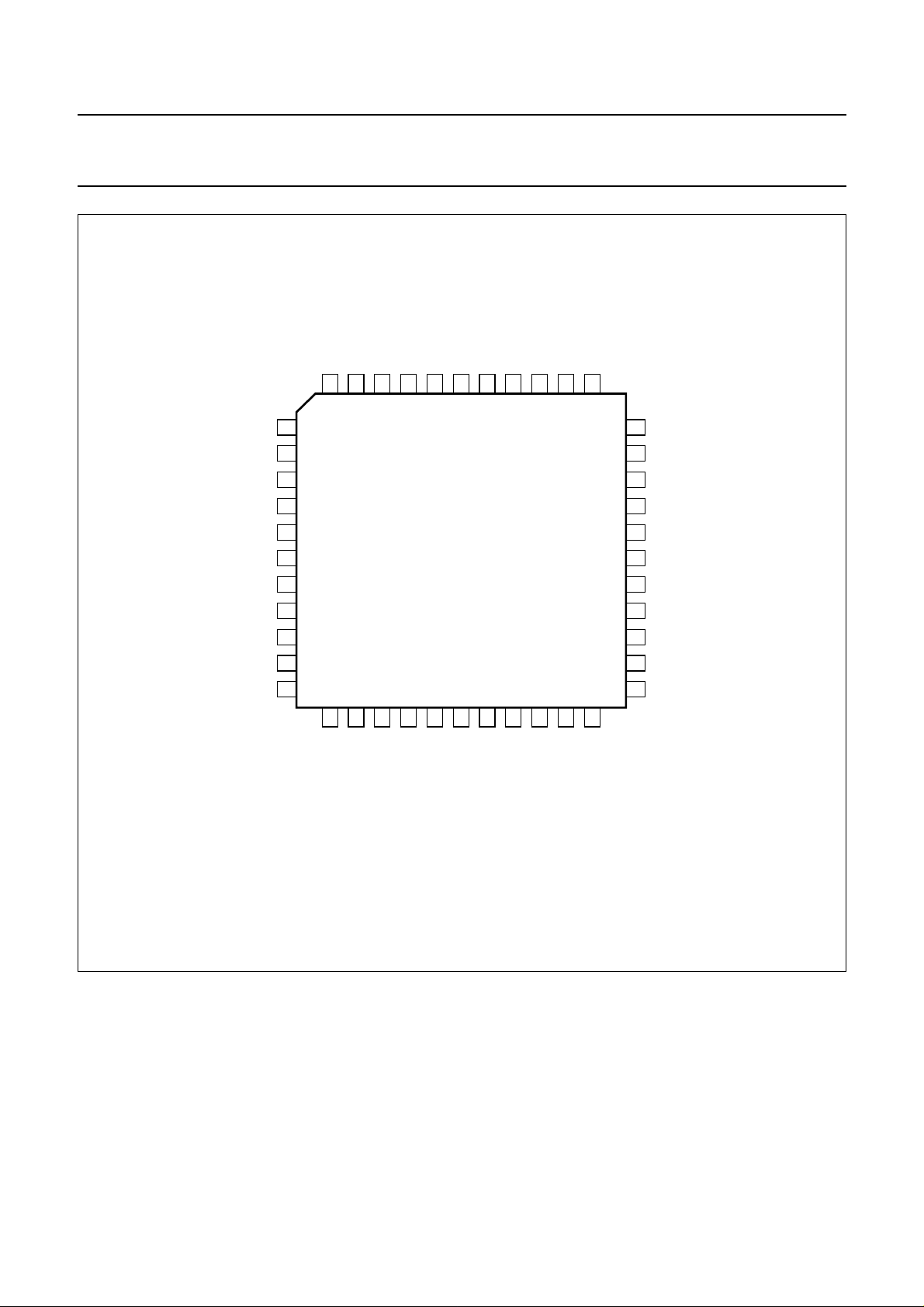
PINNING
PIN
SYMBOL
n.c. 1 − not connected
AGND 2 1 analog ground
S3 3 2 contact 3 for the step-up converter
K5 4 − output port from port extension
P03 5 3 general purpose I/O port (connected to P03)
P02 6 4 general purpose I/O port (connected to P02)
P01 7 5 general purpose I/O port (connected to P01)
n.c. 8 − not connected
P00 9 6 general purpose I/O port (connected to P00)
V
DDD
n.c. 11 − not connected
TEST1 12 8 test pin 1 (connected to P10; must be left open-circuit in the application)
P11 13 9 general purpose I/O port or interrupt (connected to P11)
P12 14 10 general purpose I/O port or interrupt (connected to P12)
P13 15 11 general purpose I/O port or interrupt (connected to P13)
P14 16 12 general purpose I/O port or interrupt (connected to P14)
n.c. 17 − not connected
P15 18 13 general purpose I/O port or interrupt (connected to P15)
P16 19 14 general purpose I/O port or interrupt (connected to P16)
TEST2 20 15 test pin 2 (connected to PSEN; must be left open-circuit in the application)
P17 21 16 general purpose I/O port or interrupt (connected to P17)
RESET 22 17 input for resetting the microcontroller (active HIGH)
n.c. 23 − not connected
n.c. 24 − not connected
n.c. 25 − not connected
n.c. 26 − not connected
n.c. 27 − not connected
RxD 28 18 serial interface receive line
TxD 29 19 serial interface transmit line
INT1 30 20 general purpose I/O port or interrupt (connected to P33)
T0 31 21 general purpose I/O port (connected to P34)
AUX1 32 22 push-pull auxiliary output (±5 mA; connected to timer T1 e.g. P35)
AUX2 33 23 push-pull auxiliary output (±5 mA; connected to timer P36)
P37 34 24 general purpose I/O port (connected to P37)
XTAL2 35 25 crystal connection
XTAL1 36 26 crystal connection or external clock input
DGND 37 27 digital ground
n.c. 38 − not connected
LQFP64
SOT314-2
10 7 digital supply voltage
QFP44
SOT307-2
DESCRIPTION
1996 Sep 25 5
Page 6
Philips Semiconductors Product specification
Low-power smart card coupler TDA8005
PIN
SYMBOL
n.c. 39 − not connected
P20 40 28 general purpose I/O port (connected to P20)
P21 41 − general purpose I/O port (connected to P21)
P22 42 29 general purpose I/O port (connected to P22)
P23 43 30 general purpose I/O port (connected to P23)
ALARM 44 − open-drain output for Power-On Reset (active HIGH or LOW by mask option)
n.c. 45 − not connected
DELAY 46 31 external capacitor connection for delayed reset signal
PRES 47 32 card presence contact input (active HIGH or LOW by mask option)
TEST3 48 33 test pin 3 (must be left open-circuit in the application)
K4 49 − output port from port extension
K3 50 − output port from port extension
K2 51 − output port from port extension
K1 52 − output port from port extension
K0 53 − output port from port extension
TEST4 54 34 test pin 4 (must be left open-circuit in the application)
I/O 55 35 data line to/from the card (ISO C7 contact)
RST 56 36 card reset output (ISO C2 contact)
CLK 57 37 clock output to the card (ISO C3 contact)
V
CC
LIS 59 39 supply for low-impedance on cards contacts
S5 60 40 contact 5 for the step-up converter
S2 61 41 contact 2 for the step-up converter
S4 62 42 contact 4 for the step-up converter
V
DDA
S1 64 44 contact 1 for the step-up converter
LQFP64
SOT314-2
58 38 card supply output voltage (ISO C1 contact)
63 43 analog supply voltage
QFP44
SOT307-2
DESCRIPTION
1996 Sep 25 6
Page 7

Philips Semiconductors Product specification
Low-power smart card coupler TDA8005
handbook, full pagewidth
V
n.c.
AGND
S3
K5
P03
P02
P01
n.c.
P00
DDD
n.c.
TEST1
P11
P12
P13
P14
DDA
VS1S4
64
63
1
2
3
4
5
6
7
8
S2
S5.
62
60
61
LIS
59
CC
V
CLK
RST
I/O
TEST4K0K1
57
56
58
55
53
54
K2
K3
K4
52
51
49
50
TEST3
48
47
PRES
46
DELAY
45
n.c.
ALARM
44
43
P23
42
P22
41
P21
TDA8005G
P20
9
10
11
12
13
14
15
16
40
39
n.c.
38
n.c.
37
DGND
36
XTAL1
35
XTAL2
34
P37
33
AUX2
21
22
17
n.c.
18
P15
19
P16
20
P17
TEST2
23
n.c.
RESET
Fig.2 Pin configuration (LQFP64; SOT314-2).
1996 Sep 25 7
24
n.c.
25
n.c.
26
n.c.
27
n.c.
28
RxD
29
TxD
30
INT1
31
T0
32
AUX1
MLD211
Page 8
Philips Semiconductors Product specification
Low-power smart card coupler TDA8005
handbook, full pagewidth
AGND
S3
P03
P02
P01
P00
V
DDD
TEST1
P11
P12
P13
DDA
S1
V
S4
S2
S5
44
43
42
41
40
1
2
3
4
5
14
P16
TDA8005H
15
16
P17
TEST2
6
7
8
9
10
11
12
13
P14
P15
LIS
39
17
RESET
CC
V
38
18
RxD
CLK
37
19
TxD
RST
36
20
INT1
I/O
35
21
T0
TEST4
34
22
AUX1
33
32
31
30
29
28
27
26
25
24
23
MLD212
TEST3
PRES
DELAY
P23
P22
P20
DGND
XTAL1
XTAL2
P37
AUX2
Fig.3 Pin configuration (QFP44; SOT307-2).
1996 Sep 25 8
Page 9

Philips Semiconductors Product specification
Low-power smart card coupler TDA8005
FUNCTIONAL DESCRIPTION
Microcontroller
The microcontroller is an 80CL51 with 256 bytes of RAM
instead of 128. The baud rate of the UART has been
multiplied by four in modes 1, 2 and 3 (which means that
the division factor of 32 in the formula is replaced by 8 in
both reception and transmission, and that in the reception
modes, only four samples per bit are taken with decision
on the majority of samples 2, 3 and 4) and the delay
counter has been reduced from 1536 to 24.
Remark: this has an impact when getting out of
PDOWN mode. It is recommended to switch to internal
clock before entering PDOWN mode
(see
“application report”
).
All the other functions remain unchanged. Please, refer to
the published specification of the 80CL51 for any further
information. Pins INT0, P10, P04 to P07 and P24 to P27
are used internally for controlling the smart card interface.
Mode 0 is unchanged. The baud rate for modes 1 and 3 is:
SMOD
2
----------------- -
×
--------------------------------------------------
8
12 256 TH1 )–(×
The baud rate for mode 2 is:
f
clk
SMOD
2
----------------- 16
f
×
clk
Table 1 Mode 3 timing
Supply
The circuit operates within a supply voltage range of
2.5 to 6 V. The supply pins are V
Pins V
and AGND supply the analog drivers to the card
DDA
, DGND and AGND.
DDD
and have to be externally decoupled because of the large
current spikes that the card and the step-up converter can
create. An integrated spike killer ensures the contacts to
the card remain inactive during power-up or power-down.
An internal voltage reference is generated which is used
within the step-up converter, the voltage supervisor, and
the V
generator.
CC
The voltage supervisor generates an alarm pulse, whose
length is defined by an external capacitor tied to the
DELAY pin, when V
is too low to ensure proper
DDD
operation (1 ms per 1 nF typical). This pulse is used as a
RESET pulse by the controller, in parallel with an external
RESET input, which can be tied to the system controller.
It is also used in order to either block any spurious card
contacts during controllers reset, or to force an automatic
deactivation of the contacts in the event of supply drop-out
[see Sections “Activation sequence” and “Deactivation
sequence (see Fig.10)”].
In the 64 pin version, this reset pulse is output to the open
drain ALARM pin, which may be selected active HIGH or
active LOW by mask option and may be used as a reset
pulse for other devices within the application.
BAUD
= 6.5 MHz;
clk
VDD=5V
f
= 3.25 MHz;
clk
VDD=5or3V
f
RATE
SMOD TH1 SMOD TH1
135416 1 255 −−
67708 0 255 1 255
45139 1 253 −−
33854 0 254 0 255
27083 1 251 −−
22569 0 253 1 253
16927 −−0 254
13542 −−1 251
11285 0 250 0 253
1996 Sep 25 9
Page 10
Philips Semiconductors Product specification
Low-power smart card coupler TDA8005
handbook, full pagewidth
V
+ V
th1
hys1
V
th1
V
DD
V
th2
V
DEL
ALARM
Fig.4 Supply supervisor.
Low impedance supply (pin LIS)
For some applications, it is mandatory that the contacts to
the card (VCC, RST, CLK and I/O) are low impedance while
the card is inactive and also when the coupler is not
powered. An auxiliary supply voltage on pin LIS ensures
this condition where I
=<5µA for V
LIS
= 5 V. This low
LIS
impedance situation is disabled when VCC starts rising
during activation, and re-enabled when the step-up
converter is stopped during deactivation. If this feature is
not required, the LIS pin must be tied to VDD.
Step-up converter
Except for the V
buffers, the whole circuit is powered by V
generator, and the other cards contacts
CC
and V
DDD
DDA
.
If the supply voltage is 3 V or 5 V, then a higher voltage is
needed for the ISO contacts supply. When a card session
is requested by the controller, the sequencer first starts the
step-up converter, which is a switched capacitors type,
clocked by an internal oscillator at a frequency
approximately 2.5 MHz. The output voltage, VUP, is
regulated at approximately 6,5 V and then fed to the V
CC
generator. VCC and GND are used as a reference for all
other cards contacts. The step-up converter may be
MBH634
chosen as a doubler or a tripler by mask option, depending
on the voltage and the current needed on the card.
ISO 7816 security
The correct sequence during activation and deactivation of
the card is ensured through a specific sequencer, clocked
by a division ratio of the internal oscillator.
Activation (START signal P05) is only possible if the card
is present (PRES HIGH or LOW according to mask
option), and if the supply voltage is correct (ALARM signal
inactive), CLK and RST are controlled by RSTIN (P04),
allowing the correct count of CLK pulses during
Answer-to-Reset from the card.
The presence of the card is signalled to the controller by
the OFF signal (P10).
During a session, the sequencer performs an automatic
emergency deactivation in the event of card take-off,
supply voltage drop, or hardware problems. The OFF
signal falls thereby warning the controller.
1996 Sep 25 10
Page 11

Philips Semiconductors Product specification
Low-power smart card coupler TDA8005
Clock circuitry
The clock to the microcontroller and the clock to the card
are derived from the main clock signal (XTAL from
2 to 16 MHz, or an external clock signal).
Microcontroller clock (f
reduction modes, the microcontroller is clocked with f
) after reset, and during power
clk
INT
/8,
which is always present because it is derived from the
internal oscillator and gives the lowest power
consumption. When required, (for card session, serial
communication or anything else) the microcontroller may
choose to clock itself with
xtal
xtal
or1⁄2f
INT
.
1
⁄2f
,1⁄4f
All frequency changes are synchronous, thereby ensuring
no hang-up due to short spikes etc.
Cards clock: the microcontroller may select to send the
card1⁄2f
xtal
,1⁄4f
xtal
,1⁄8f
xtal
or1⁄2f
(≈1.25 MHz), or to stop
INT
the clock HIGH or LOW. All transition are synchronous,
ensuring correct pulse length during start or change in
accordance with ISO 7816.
After power on, CLK is set at STOP LOW, and f
1
⁄8f
INT.
is set at
clk
Power-down and sleep modes
The TDA8005 offers a large flexibility for defining power
reduction modes by software. Some configurations are
described below.
In the power-down mode, the microcontroller is in
power-down and the supply and the internal oscillator are
active. The card is not active; this is the smallest power
consumption mode. Any change on P1 ports or on PRES
will wake-up the circuit (for example, a key pressed on the
keyboard, the card inserted or taken off).
In the sleep mode, the card is powered, but configured in
the Idle or sleep mode. The step-up converter will only be
active when it is necessary to reactivate V
. When the
UP
microcontroller is in Power-down mode any change on P1
ports or on PRES will wake up the circuit.
In both power reduction modes the sequencer is active,
allowing automatic emergency deactivation in the event of
card take-off, hardware problems, or supply drop-out.
The TDA8005 is set into Power-down or sleep mode by
software. There are several ways to return to normal
mode, Introduction or extraction of the card, detection of a
change on P1 (which can be a key pressed) or a command
from the system microcontroller. For example, if the
system monitors the clock on XTAL1, it may stop this clock
after setting the device into power-down mode and then
wake it up when sending the clock again. In this situation,
the internal clock should have been chosen before the f
clk
Peripheral interface
This block allows synchronous serial communication with
the three peripherals (ISO UART, CLOCK CIRCUITRY
and OUTPUT PORTS EXTENSION).
.
handbook, full pagewidth
RESET
CC0 CC1 CC2 CC3 CC4 CC5 CC6 CC7
UC0
UT0
PE0
P24
DATA
clock configuration
Uart configuration
UC1 UC2 UC3 UC4 UC5 UC6 UC7
Uart transmit
UT1 UT2 UT3 UT4 UT5 UT6 UT7
ports extension
PE1 PE2 PE3 PE4 PE5 PE6 PE7
P06
STROBE
P07
ENABLE
PERIPHERAL CONTROL
P27
REG0
Fig.5 Peripheral interface diagram.
1996 Sep 25 11
P26
REG1
P25
R/W
UR1 UR2 UR3 UR4 UR5 UR6 UR7
UR0
US1 US2 US3 US4 US5 US6 US7
US0
P32
INT
Uart receive
Uart status register
MBH635
Page 12

Philips Semiconductors Product specification
Low-power smart card coupler TDA8005
Table 2 Description of Fig.5
BIT NAME DESCRIPTION
REG0 = 0, REG1 = 0, R/W = 0; CLOCK CONFIGURATION
(Configuration after reset is cards clock STOP LOW, f
CC0 cards clock =
CC1 cards clock =1⁄4f
CC2 cards clock =1⁄8f
CC3 cards clock =1⁄2f
1
⁄2f
xtal
xtal
xtal
INT
CC4 cards clock = STOP HIGH
CC5 f
CC6 f
CC7 f
clk
clk
clk
=1⁄2f
=1⁄4f
=1⁄2f
xtal
xtal
INT
REG0 = 1, REG1 = 0, R/W = 0; UART CONFIGURATION (after reset all bits are cleared)
UC0 ISO UART RESET
UC1 START SESSION
UC2 LCT (Last Character to Transmit)
UC3 TRANSMIT/RECEIVE
UC4 to UC7 not used
clk
=1⁄8f
INT
)
REG0 = 0, REG1 = 1, R/W = 0; UART TRANSMIT
UT0 to UT7 LSB to MSB of the character to be transmitted to the card
REG0 = 1, REG1 = 1, R/W = 0; PORTS EXTENSION (after reset all bits are cleared)
PE0 to PE5 PE0 to PE5 is the inverse of the value to be written on K0 to K5
PE6, PE7 not used
REG0 = 0, REG1 = 0, R/W = 1; UART RECEIVE
UR0 to UR7 LSB to MSB of the character received from the card
REG0 = 1, REG1 = 0, R/W = 1; UART STATUS REGISTER (after reset all bits are cleared)
US0 UART TRANSMIT buffer empty
US1 UART RECEIVE buffer full
US2 first start bit detected
US3 parity error detected during reception of a character (the UART has asked the card to repeat the
character)
US4 parity error detected during transmission of a character. The controller must write the previous
character in UART TRANSMIT, or abort the session.
US5 to US7 not used
1996 Sep 25 12
Page 13

Philips Semiconductors Product specification
Low-power smart card coupler TDA8005
USE OF PERIPHERAL INTERFACE
Write operation:
Select the correct register with R/W, REG0, REG1.
Write the word in the peripheral shift register (PSR) with
DATA and STROBE. DATA is shifted on the rising edge
of STROBE. 8 shifts are necessary.
Give a negative pulse on ENABLE. The data is parallel
loaded in the register on the falling edge of ENABLE.
Table 3 Example of peripheral interface
CHANGE OF CLOCK CONFIGURATION
CLR REG0 CLR REG0
CLR REG1 CLR REG1
CLR R/W SET R/W
MOV R2, #8 CLR ENABLE
LOOP RRC A SET ENABLE
MOV DATA C CLR ENABLE
CLR STROBE SET ENABLE
SET STROBE MOV R2, #8
DJNZ R2, LOOP LOOP MOV C, DATA
CLR ENABLE RRC A
SET ENABLE CLR STROBE
SET DATA SET STROBE
RET DJNZ R2, LOOP
(1)
Read operation:
Select the correct register with R/W, REG0 and REG1.
Give a first negative pulse on ENABLE. The word is
parallel loaded in the peripheral shift register on the
rising edge of ENABLE.
Give a second negative pulse on ENABLE for
configuring the PSR in shift right mode.
Read the word from PSR with DATA and STROBE.
DATA is shifted on the rising edge of STROBE. 7 shifts
are necessary.
READ CHARACTER ARRIVED IN UART RECEIVE
SET DATA
RET
(2)
Notes
1. The new configuration is supposed to be in the accumulator.
2. The character will be in the accumulator.
1996 Sep 25 13
Page 14

Philips Semiconductors Product specification
Low-power smart card coupler TDA8005
ISO UART
The ISO UART handles all the specific requirements
defined in ISO T = 0 protocol type. It is clocked with the
cards clock, which gives the f
/31 sampling rate for start
clk
bit detection (the start bit is detected at the first LOW level
on I/O) and the f
/372 frequency for ETU timing (in the
clk
reception mode the bit is sampled at1⁄2ETU). It also allows
the cards clock frequency changes without interfering with
the baud rate.
This hardware UART allows operating of the
microcontroller at low frequency, thus lowering EM
radiations and power consumption. It also frees the
microcontroller of fastidious conversions and real time jobs
thereby allowing the control of higher level tasks.
The following occurs in the reception mode (see Fig.6):
• Detection of the inverse or direct convention at the begin
of ATR.
• Automatic convention setting, so the microcontroller
only receives characters in direct convention.
• Parity checking and automatic request for character
repetition in case of error (reception is possible at
12 ETU).
In the transmission mode (see Fig.7):
• Transmission according to the convention detected
during ATR, consequently the microcontroller only has
to send characters in direct convention. Transmission of
the next character may start at 12 ETU in the event of no
error or 13 ETU in case of error.
• Parity calculation and detection of repetition request
from the card in the event of error.
• The bit LCT (Last Character to Transmit) allows fast
reconfiguration for receiving the answer 12 ETU after
the start bit of the last transmitted character.
The ISO UART configuration register enables the
microcontroller to configure the ISO UART. cf Peripheral
Interface.
After power-on, all ISO UART registers are reset.
The ISO UART is configured in the reception mode. When
the microcontroller wants to start a session, it sets the bits
START SESSION and RESET ISO UART in UART
CONFIGURATION and then sets START LOW. When the
first start bit on I/O is detected (sampling rate f
/31), the
clk
UART sets the bit US2 (First Start Detect) in the status
register which gives an interrupt on INT0 one CLK pulse
later.
The convention is recognized on the first character of the
ATR and the UART configures itself in order to exchange
direct data without parity processing with the
microcontroller whatever the convention of the card is.
The bit START SESSION must be reset by software. At
the end of every character, the UART tests the parity and
resets what is necessary for receiving another character.
If no parity error is detected, the UART sets the bit US1
(BUFFER FULL) in the STATUS REGISTER which warns
the microcontroller it has to read the character before the
reception of the next one has been completed. The
STATUS REGISTER is reset when read from the
controller.
If a parity error has been detected, the UART pulls the I/O
line LOW between 10.5 and 12 ETU. It also sets the bits
BUFFER FULL and US3 (parity error during reception) in
the STATUS REGISTER which warns the microcontroller
that an error has occurred. The card is supposed to repeat
the previous character.
The ISO UART status register can inform which event has
caused an interrupt. (Buffer full, buffer empty, parity error
detected etc.) cf Peripheral Interface.
This register is reset when the microcontroller reads the
status out of it.
1996 Sep 25 14
Page 15

Philips Semiconductors Product specification
Low-power smart card coupler TDA8005
handbook, full pagewidth
T/R = 0
or
LCT = 1
start session ↑ and T/R = 0
SET ENABLE FSD
clock starts
INHIBIT I/O DURING 200 CLK
SAMPLE I/O EVERY 31 CLK
I/O = 0
SAMPLE I/O AT 186
AND EVERY 372 CLK
10th bit
CONVERT AND LOAD CHARACTER
IN RECEPTION BUFFER AT 10 ETU
CHECK PARITY
DISABLE I/O BUFFER BETWEEN
10 AND 12 ETU
5th bit
parity error
SET FSD STATUS REGISTER
IN FSD IS ENABLED
RESET EN FSD
SET CONVENTION
IF START SESSION = 1
SET BIT RECEPTION PARITY
ERROR AT 10 ETU
PULL I/O LINE LOW FROM
10.5 TILL 11.75 ETU
(1)
SET BIT BUFFER FULL AT 10 ETU
RESET RECEPTION PART AT 12 ETU
T/R =1
(1) The start session is reset by software.
(2) The software may load the received character in the peripheral
control at any time without any action on the ISO UART.
Fig.6 ISO UART reception flow chart.
When the controller needs to transmit data to the card, it
first sets the bit UC3 in the UART CONFIGURATION
which configures the UART in the transmission mode.
As soon as a character has been written in the UART
TRANSMIT register, the UART makes the conversion,
1996 Sep 25 15
(2)
MBH636
calculates the parity and starts the transmission on the
rising edge of ENABLE. When the character has been
transmitted, it surveys the I/O line at 11 ETU in order to
know if an error has been detected by the card.
Page 16

Philips Semiconductors Product specification
Low-power smart card coupler TDA8005
If no error has occurred, the UART sets the bit US0
(BUFFER EMPTY) in the STATUS REGISTER and waits
for the next character. If the next character has been
written before 12 ETU, the transmission will start at
12 ETU. If it was written after 12 ETU it will start on the
rising edge of ENABLE.
If an error has occurred, it sets the bits BUFFER EMPTY
and US4 (parity error during transmission) which warns
the microcontroller to rewrite the previous character in the
UART TRANSMIT register. If the character has been
rewritten before 13 ETU, the transmission will start at
handbook, full pagewidth
transmit register selected
CONVERT, CALCULATE PARITY
T/R ↑
SET TRANSMIT ENABLE
AND LOAD IN TRANSMIT
SHIFT REGISTER
13 ETU. If it has been written after 13 ETU it will start on
the rising edge of ENABLE.
When the transmission is completed, the microcontroller
may set the bit LCT (Last Character to Transmit) so that
the UART will force the reception mode into ready to get
the reply from the card at 12 ETU. This bit must be reset
before the end of the first reception. The bit T/R must be
reset to enable the reception of the following characters.
When the session is completed, the microcontroller
re-initializes the whole UART by resetting the bit RESET
ISO UART.
(1)
SHIFT EVERY ETU IF TRANSMIT
ENABLE IS SET
10th bit shifted
SET I/O BUFFER IN
RECEPTION AT 10 ETU
SAMPLE I/O AT 11 ETU
SET BIT BUFFER EMPTY
AT 11 ETU
LCT = 1
RESET TRANSMIT PART AT 11 ETU
FORCE RECEPTION MODE
(1) The transmit register may be loaded just after reading from the status register.
(2) The software must reset the last character but before completion of the first received character.
RESET TRANSMIT PART AND
ENABLE TRANSMIT AT 12 ETU
T/R = 0
parity error
(2)
Fig.7 ISO UART transmission flow chart.
SET BIT TRANSMISSION PARITY
ERROR AND BUFFER EMPTY
AT 11 ETU
RESET TRANSMIT PART AND
ENABLE TRANSMIT AT 13 ETU
MBH637
1996 Sep 25 16
Page 17

Philips Semiconductors Product specification
Low-power smart card coupler TDA8005
I/O buffer modes (see Fig.8) The following are the I/O buffer modes:
1. I/O buffer disabled by ENIO.
2. I/O buffer in input, 20 kΩ pull-up resister connected
between I/O and VCC, I/O masked till 200 clock pulses.
3. I/O buffer in input, 20 kΩ pull-up resister connected
between I/O and VCC, I/O is sampled every 31 clock
pulses.
4. I/O buffer in output, 20 kΩ pull-up resister connected
between I/O and VCC.
5. I/O buffer in output, I/O is pulled LOW by the N
transistor of the buffer.
6. I/O buffer in output, I/O is strongly HIGH or LOW by the
P or N transistor.
Output ports extension
In the LQFP64 version, 6 auxiliary output ports may be
used for low frequency tasks (for example, keyboard
scanning). These ports are push-pull output types (cf use
in software document).
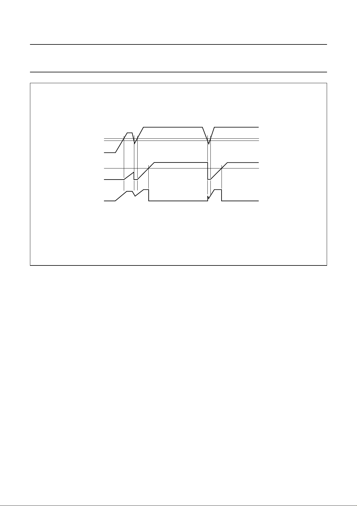
Activation sequence
When the card is inactive, V
, CLK, RST and I/O are
CC
LOW, with low impedance with respect to GND. The
step-up converter is stopped. The I/O is configured in the
reception mode with a high impedance path to the ISO
UART, subsequently no spurious pulse from the card
during power-up will be taken into account until I/O is
enabled. When everything is satisfactory (voltage supply,
card present, no hardware problems), the microcontroller
may initiate an activation sequence by setting START
LOW (t0):
• The step-up converter is started (t1)
• LIS signal is disabled by ENLI, and VCC starts rising from
0 to 5 V with a controlled rise time of 0.1 V/µs typically
(t2)
• I/O buffer is enabled (t3)
• Clock is sent to the card (t4)
• RST buffer is enabled (t5).
In order to allow a precise count of clock pulses during
ATR, a defined time window (t
; t5) is opened where the
3
clock may be sent to the card by means of RSTIN. Beyond
this window, RSTIN has no more action on clock, and only
monitors the cards RST contact (RST is the inverse of
RSTIN).
The sequencer is clocked by f
/64 which leads to a time
INT
interval T of 25 µs typical. Thus t1=0to1⁄64T,
t2=t1+1⁄23T, t3=t1+ 4T, t4=t3to t5 and t5=t1+7T
(see Fig.9).
Deactivation sequence (see Fig.10) When the session is completed, the microcontroller sets
START HIGH. The circuit then executes an automatic
deactivation sequence:
• Card reset (RST falls LOW) at t
• Clock is stopped at t
11
10
• I/O becomes high impedance to the ISO UART (t12)
• VCC falls to 0 V with typical 0.1 V/µs slew rate (t13)
• The step-up converter is stopped and CLK, RST, V
CC
and I/O become low impedance to GND (t14).
• t10<1⁄64T; t11=t10+1⁄2T; t12=t10+ T; t13=t10+1⁄23T;
t14=t10+ 5T.
Protections
Main hardware fault conditions are monitored by the circuit
• Overcurrent on V
CC
• Short circuits between VCC and other contacts
• Card take-off during transaction.
When one of these problems is detected, the security logic
block pulls the interrupt line OFF LOW, in order to warn the
microcontroller, and initiates an automatic deactivation of
the contacts. When the deactivation has been completed,
the OFF line returns HIGH, except if the problem was due
to a card extraction in which case it remains LOW till a card
is inserted.
1996 Sep 25 17
Page 18

Philips Semiconductors Product specification
Low-power smart card coupler TDA8005
handbook, full pagewidth
I/O
MODE
OUT
IN
T
R
PRES
I/O BUFFER
ISO UART
handbook, full pagewidth
activation character
12 34543416363343 1
character
reception
with error
character
reception
without
error
character
transmission
with error
character
transmission
without
error
reception
without
error
forced
deactivation
MBH638
Fig.8 I/O buffer modes.
t
act
OFF
START
f
/64
INT
V
UP
V
CC
I/O
ENRST
RSTIN
CLK
RST
ENLI
internal
internal
t
3
t
5
Fig.9 Activation sequence.
MBH639
1996 Sep 25 18
Page 19

Philips Semiconductors Product specification
Low-power smart card coupler TDA8005
handbook, full pagewidth
PRES
OFF
START
f
/64
INT
RST
CLK
I/O
V
CC
V
UP
ENLI
internal
t10t11t12t
13
t
de
t
14
Fig.10 Emergency deactivation sequence after a card take-off.
MBH640
1996 Sep 25 19
Page 20

Philips Semiconductors Product specification
Low-power smart card coupler TDA8005
LIMITING VALUES
In accordance with the Absolute Maximum Rating System (IEC 134).
SYMBOL PARAMETER CONDITIONS MIN. MAX. UNIT
V
DDA
V
DDD
V
n
I
n1
I
n2
I
n3
I
n4
I
n5
I
n6
I
n7
P
tot
T
stg
V
es
T
j
analog supply voltage −0 6.5 V
digital supply voltage −0 6.5 V
all input voltages −0V
DC current into XTAL1, XTAL2, RX, TX,
− 5mA
+ 0.5 V
DD
RESET, INT1, P34, P37, P00 to P03,
P11 to P17, P20 to P23 and
TEST1 to TEST4
DC current from or to AUX1, AUX2 −10 +10 mA
DC current from or to S1 to S5 −30 +30 mA
DC current into DELAY −5 +10 mA
DC current from or to PRES −5+5mA
DC current from and to K0 to K5 −5+5mA
DC current from or into ALARM
−5+5mA
(according to option choice)
continuous total power dissipation T
IC storage temperature −55 +150
electrostatic discharge on pins I/O, VCC,
= −20 to +85°C − 500 mW
amb
−6+6kV
o
C
RST, CLK and PRES
on other pins −2+2kV
Operating Junction Temp. −−125 °C
HANDLING
Inputs and outputs are protected against electrostatic discharge in normal handling. However, to be totally safe, it is
desirable to take normal precautions appropriate to handling MOS devices.
THERMAL CHARACTERISTICS
SYMBOL PARAMETER VALUE UNIT
R
th j-a
from junction to ambient in free air
LQFP64 70 K/W
QFP44 60 K/W
1996 Sep 25 20
Page 21

Philips Semiconductors Product specification
Low-power smart card coupler TDA8005
CHARACTERISTICS
V
=5V; VSS=0V; T
DD
SYMBOL PARAMETER CONDITIONS MIN. TYP. MAX. UNIT
Supply
V
DD
I
DD(pd)
supply voltage Option dependant 2.5 − 6.0 V
supply current power-down
mode
I
DD(sm)
I
DD(om)
V
th1
supply current sleep mode card powered, but with clock
supply current operating mode unloaded; f
threshold voltage on V
(falling)
V
V
V
I
DEL
t
W
hys1
th2
DEL
hysteresis on V
threshold voltage on DELAY − 1.38 − V
voltage on pin DELAY 4.6 − V
output current at DELAY pin grounded (charge) −1.5 −1 −0.4 µA
ALARM pulse width C
ALARM (open drain active HIGH or LOW output)
I
V
I
V
OH
OL
OL
OH
HIGH level output current active LOW option; VOH=5V −−10 µA
LOW level output voltage active LOW option; IOL=2mA −−0.4 V
LOW level output current active HIGH option, VOL=0V −−−10 µA
HIGH level output voltage active HIGH option, IOH= −2mA VDD− 1 −− V
Crystal oscillator (note 1)
f
xtal
f
EXT
crystal frequency 2 − 16 MHz
external frequency applied on
XTAL1
=25°C; for general purpose I/O ports see 80CL51 data sheet; unless otherwise specified.
amb
VDD= 5 V; card inactive
− 90 −µA
VDD=3V; “ “
− 500 −µA
stopped
DD
= 13 MHz;
xtal
f
= 6.5 MHz; f
clk
V
=3V; f
DD
f
= 3.25 MHz; f
clk
xtal
= 3.25 MHz
card
= 13 MHz;
= 3.25 MHz
card
supervisor option 2 − 2.3 V
− 5.5 − mA
− 3 − mA
2.45 − 3V
3.8 − 4.5 V
th1
V
DEL=VDD
DEL
(discharge) 4 6.8 10 mA
=10nF − 10 − ms
40 − 350 mV
DD
0 − 16 MHz
V
Step-up converter
f
V
INT
UP
oscillation frequency 2 − 3 MHz
voltage on S5 − 6.5 − V
Low impedance supply (LIS)
V
I
LIS
LIS
voltage on LIS 0 − V
current at LIS −−7µA
1996 Sep 25 21
DD
V
Page 22

Philips Semiconductors Product specification
Low-power smart card coupler TDA8005
SYMBOL PARAMETER CONDITIONS MIN. TYP. MAX. UNIT
Reset output to the card (RST)
V
inactive
I
inactive
V
OL
V
OH
t
r
t
f
Clock output to the card (CLK)
V
inactive
I
inactive
V
OL
V
OH
t
r
t
f
f
clk
δ duty cycle CL=30pF 45 − 55 %
output voltage when inactive −0.3 − 0.4 V
when LIS is used; I
current from RST when
=1mA −0.3 − 0.4 V
inactive
−−−1mA
inactive and pin grounded
LOW level output voltage IOL= 200 µA −0.25 − 0.4 V
HIGH level output voltage IOH<−200 µA4−V
+ 0.3 V
CC
rise time CL=30pF −−1µs
fall time CL=30pF −−1µs
output voltage when inactive −0.3 − 0.4 V
when LIS is used; I
current from CLK when
=1mA −0.3 − 0.4 V
inactive
−−−1mA
inactive and pin grounded
LOW level output voltage IOL= 200 µA −0.25 − 0.4 V
HIGH level output voltage IOH<−200 µAV
−0.5 − VCC+0.25 V
CC
rise time CL=30pF −−15 ns
fall time CL=30pF −−15 ns
clock frequency 1 MHz Idle configuration 1 − 1.5 MHz
low operating speed −−2 MHz
middle operating speed −−4 MHz
high operating speed −−8 MHz
Card supply voltage (V
V
inactive
output voltage when inactive −0.3 − 0.4 V
CC
)
when LIS is used; I
I
inactive
current from VCC when
inactive and pin grounded
V
cc
output voltage in active mode
with 100 nF capacitor;
I
= 200 mA, f
max
duration <400 ns
static load (up to 20 mA)
dynamic current of 40 nA
I
CC
output current VCC = 5V −−−20 mA
V
shorted to GND −−−40 mA
CC
SR slew rate up or down
(max capacitance is 150 nF)
1996 Sep 25 22
inactive
= 5 MHz, and
max
=1mA −0.3 − 0.4 V
−−−1mA
−
4.75
4.5
−−
5.25
5.5
0.04 0.1 0.16 V/µs
V
Page 23

Philips Semiconductors Product specification
Low-power smart card coupler TDA8005
SYMBOL PARAMETER CONDITIONS MIN. TYP. MAX. UNIT
Data line (I/O)
V
inactive
I
inactive
V
OL
V
OH
V
IL
V
IH
t
r
t
f
R
pu
output voltage when inactive −0.3 − 0.4 V
when LIS is used; I
current from I/O when inactive
=1mA −0.3 − 0.4 V
inactive
−−−1mA
and pin grounded
LOW level output voltage (I/O
IOL=1mA −0.25 − 0.3 V
configured as an output)
HIGH level output voltage (I/O
IOH<−100 µAV
+0.8 − VCC+0.25 V
CC
configured as an output)
input voltage LOW (I/O
IIL= 1 mA 0 − 0.5 V
configured as an input)
input voltage HIGH (I/O
IIL= 100 µAV
+0.6 − V
CC
CC
V
configured as an input)
rise time CL=30pF −−1µs
fall time CL=30pF −−1µs
pull-up resistor connected to
see Table 4 for options −−−
VCC when I/O is input
Protections
I
CC(sd)
shutdown current at V
CC
Timing
t
act
t
de
activation sequence duration −−225 µs
deactivation sequence
duration
t
3(start)
start of the window for sending
clock to the card
t
5(end)
end of the window for sending
clock to the card
Auxiliary outputs (AUX1, AUX2)
V
OL
V
OH
LOW level output voltage IOL=5mA −−0.4 V
HIGH level output voltage IOH= −5mA VDD− 1 −− V
Output ports from extension (K0 to Kn)
V
OL
V
OH
LOW level output voltage IOL=2mA −−0.4 V
HIGH level output voltage IOH= −2mA VDD− 1 −− V
Card presence input (PRES)
V
IL
V
IH
I
IH
LOW level input voltage IIL= −1mA −−0.6 V
HIGH level input voltage IIH= 100 µA 0.7V
HIGH level input current VIH=+5V 0.2 − 3 µA
Note
1. The crystal oscillator is the same as OPTION 3 of the 80CL51.
−−30 − mA
−−150 µs
−−130 µs
140 −− µs
DD
−− V
1996 Sep 25 23
Page 24

1996 Sep 25 24
KEYBOARD
5 V
(analog)
1615141312111098765432
100 nF
5 V(analog)
1
100 nF
APPLICATION INFORMATION
Philips Semiconductors Product specification
Low-power smart card coupler TDA8005
5 V(logic)
MMI-CLK
MMI-REQ
from
system
controller
RESET
RX
TX
MMI-EN
LIS
LED2
LED1
R7
1.5 Ω
1.5 Ω
R8
17
18
19
20
21
22
23
24
25
26
27
28
29
30
31
32
333435363738394041424344454647
TDA8005G
4.7
nF
64
63
62
61
60
59
58
57
56
55
54
53
52
51
50
49
48
47 nF
4.7
nF
100
nF
5 V(logic)
100
kΩ
NC8
NC7
NC6
NC5
C1
C2
C3
C4
CARD-READ-C702
K1
K2
NC1
NC2
NC3
NC4
C5
C6
C7
C8
MGC440
handbook, full pagewidth
Fig.11 Possible GSM application.
Page 25

1996 Sep 25 25
n
KEYBOARD
dbook, full pagewidth
Philips Semiconductors Product specification
Low-power smart card coupler TDA8005
V
DD
4.7
nF
47 nF
1
48
100 nF
64
63
62
61
60
59
58
57
56
55
54
53
52
51
50
49
47 nF
47
nF
3 V
100
nF
C8
C7
C6
C5
NC1
NC2
NC3
NC4
CARD-READ-LM01
K1
K2
C4
C3
C2
C1
NC5
NC6
NC7
NC8
MGC439
100 nF
1615141312111098765432
17
18
19
20
21
22
23
24
25
26
27
28
29
30
31
32
333435363738394041424344454647
33
pF
7.15
MHz
DD
LED1
LED2
R6
R7
V
TDA8005G
33
pF
R/W
AS E D7 D6 D5 D4 D3 D2 D1 D8
DISPLAY DRIVER
AND DISPLAY
Fig.12 Possible stand-alone application.
Page 26

Philips Semiconductors Product specification
Low-power smart card coupler TDA8005
Table 4 TDA8005 option choice form
FUNCTION DESCRIPTION OPTION
Ports
P00
P01
P02
P03
P04 RSTIN (fixed) 3 S
P05 START (fixed) 3 S
P06 STR (fixed) 3 S
P07 EN (fixed) 3 S
P10 OFF (fixed) 2 S
P11
P12
P13
P14
P15
P16
P17
P20
P21
P22
P23
P24 DATA (fixed) 1 S
P25 R/W (fixed) 3 S
P26 REG1 (fixed) 3 S
P27 REG0 (fixed) 3 S
P30
P31
P32 INT (fixed) 1 S
P33
P34
P35 AUXI (fixed) 3 S
P36 AUX2 (fixed) 3 S
P37
FUNCTION DESCRIPTION OPTION
Analog options
Step-up doubler (updo) or tripler
(uptri)
Supervisor 2.3 (supervb, 3 (supervtr) or
4.5 (superVCI)
I/O low impedance (UARTl) or
high impedance (UARTZ)
I/O pull-up 10, 20 or 30 kΩ
R_CLK 0, 50, 100, 150 or 200 Ω
R_RST 0, 50, 80, 130 or 180 Ω
ALARM active HIGH (alarmbufp) or
active LOW (alarmbufn)
PRES active HIGH (prestopp) or
active LOW (prestopn)
1996 Sep 25 26
Page 27

Philips Semiconductors Product specification
Low-power smart card coupler TDA8005
PACKAGE OUTLINES
LQFP64: plastic low profile quad flat package; 64 leads; body 10 x 10 x 1.4 mm
c
y
X
A
48 33
49
64
pin 1 index
1
16
Z
32
E
e
H
E
E
A
2
A
A
1
w M
b
p
17
detail X
SOT314-2
(A )
3
θ
L
p
L
Z
e
w M
b
p
D
D
H
D
v M
B
v M
0 2.5 5 mm
scale
DIMENSIONS (mm are the original dimensions)
UNIT
mm
A
A1A2A3b
max.
0.20
1.60
0.05
1.45
1.35
0.25
cE
p
0.27
0.18
0.17
0.12
(1)
(1) (1)(1)
D
10.1
9.9
eH
10.1
9.9
0.5
12.15
11.85
Note
1. Plastic or metal protrusions of 0.25 mm maximum per side are not included.
OUTLINE
VERSION
IEC JEDEC EIAJ
REFERENCES
SOT314-2
1996 Sep 25 27
A
B
E
12.15
11.85
LL
p
0.75
0.45
0.12 0.11.0 0.2
H
D
EUROPEAN
PROJECTION
Z
1.45
1.05
D
Zywv θ
E
o
1.45
7
o
1.05
0
ISSUE DATE
95-12-19
97-08-01
Page 28

Philips Semiconductors Product specification
Low-power smart card coupler TDA8005
QFP44: plastic quad flat package; 44 leads (lead length 1.3 mm); body 10 x 10 x 1.75 mm
c
y
X
A
33 23
34
pin 1 index
44
1
22
Z
E
e
H
E
E
w M
b
p
12
11
A
2
A
A
1
detail X
SOT307-2
(A )
3
θ
L
p
L
w M
b
e
p
D
H
D
Z
D
B
0 2.5 5 mm
scale
DIMENSIONS (mm are the original dimensions)
mm
A
max.
2.10
0.25
0.05
1.85
1.65
0.25
UNIT A1A2A3b
cE
p
0.40
0.25
0.20
0.14
(1)
(1) (1)(1)
D
10.1
9.9
eH
10.1
9.9
12.9
0.8 1.3
12.3
Note
1. Plastic or metal protrusions of 0.25 mm maximum per side are not included.
OUTLINE
VERSION
IEC JEDEC EIAJ
REFERENCES
SOT307-2
1996 Sep 25 28
v M
H
v M
D
A
B
E
12.9
12.3
LL
p
0.95
0.55
0.15 0.10.15
EUROPEAN
PROJECTION
Z
D
1.2
0.8
Zywv θ
E
o
1.2
10
o
0.8
0
ISSUE DATE
95-02-04
97-08-01
Page 29

Philips Semiconductors Product specification
Low-power smart card coupler TDA8005
SOLDERING
Introduction
There is no soldering method that is ideal for all IC
packages. Wave soldering is often preferred when
through-hole and surface mounted components are mixed
on one printed-circuit board. However, wave soldering is
not always suitable for surface mounted ICs, or for
printed-circuits with high population densities. In these
situations reflow soldering is often used.
This text gives a very brief insight to a complex technology.
A more in-depth account of soldering ICs can be found in
our
“IC Package Databook”
Reflow soldering
Reflow soldering techniques are suitable for all LQFP and
QFP packages.
The choice of heating method may be influenced by larger
plastic QFP packages (44 leads, or more). If infrared or
vapour phase heating is used and the large packages are
not absolutely dry (less than 0.1% moisture content by
weight), vaporization of the small amount of moisture in
them can cause cracking of the plastic body. For more
information, refer to the Drypack chapter in our
Reference Handbook”
Reflow soldering requires solder paste (a suspension of
fine solder particles, flux and binding agent) to be applied
to the printed-circuit board by screen printing, stencilling or
pressure-syringe dispensing before package placement.
Several techniques exist for reflowing; for example,
thermal conduction by heated belt. Dwell times vary
between 50 and 300 seconds depending on heating
method. Typical reflow temperatures range from
215 to 250 °C.
(order code 9398 652 90011).
“Quality
(order code 9397 750 00192).
Wave soldering
Wave soldering is not recommended for LQFP or QFP
packages. This is because of the likelihood of solder
bridging due to closely-spaced leads and the possibility of
incomplete solder penetration in multi-lead devices.
If wave soldering cannot be avoided, the following
conditions must be observed:
• A double-wave (a turbulent wave with high upward
pressure followed by a smooth laminar wave)
soldering technique should be used.
• The footprint must be at an angle of 45° to the board
direction and must incorporate solder thieves
downstream and at the side corners.
Even with these conditions:
• Do not consider wave soldering LQFP packages
LQFP48 (SOT313-2), LQFP64 (SOT314-2) or
LQFP80 (SOT315-1).
• Do not consider wave soldering QFP packages
QFP52 (SOT379-1), QFP100 (SOT317-1),
QFP100 (SOT317-2), QFP100 (SOT382-1) or
QFP160 (SOT322-1).
During placement and before soldering, the package must
be fixed with a droplet of adhesive. The adhesive can be
applied by screen printing, pin transfer or syringe
dispensing. The package can be soldered after the
adhesive is cured.
Maximum permissible solder temperature is 260 °C, and
maximum duration of package immersion in solder is
10 seconds, if cooled to less than 150 °C within
6 seconds. Typical dwell time is 4 seconds at 250 °C.
A mildly-activated flux will eliminate the need for removal
of corrosive residues in most applications.
Preheating is necessary to dry the paste and evaporate
the binding agent. Preheating duration: 45 minutes at
45 °C.
1996 Sep 25 29
Repairing soldered joints
Fix the component by first soldering two diagonallyopposite end leads. Use only a low voltage soldering iron
(less than 24 V) applied to the flat part of the lead. Contact
time must be limited to 10 seconds at up to 300 °C. When
using a dedicated tool, all other leads can be soldered in
one operation within 2 to 5 seconds between
270 and 320 °C.
Page 30

Philips Semiconductors Product specification
Low-power smart card coupler TDA8005
DEFINITIONS
Data sheet status
Objective specification This data sheet contains target or goal specifications for product development.
Preliminary specification This data sheet contains preliminary data; supplementary data may be published later.
Product specification This data sheet contains final product specifications.
Limiting values
Limiting values given are in accordance with the Absolute Maximum Rating System (IEC 134). Stress above one or
more of the limiting values may cause permanent damage to the device. These are stress ratings only and operation
of the device at these or at any other conditions above those given in the Characteristics sections of the specification
is not implied. Exposure to limiting values for extended periods may affect device reliability.
Application information
Where application information is given, it is advisory and does not form part of the specification.
LIFE SUPPORT APPLICATIONS
These products are not designed for use in life support appliances, devices, or systems where malfunction of these
products can reasonably be expected to result in personal injury. Philips customers using or selling these products for
use in such applications do so at their own risk and agree to fully indemnify Philips for any damages resulting from such
improper use or sale.
1996 Sep 25 30
Page 31

Philips Semiconductors Product specification
Low-power smart card coupler TDA8005
NOTES
1996 Sep 25 31
Page 32

Philips Semiconductors – a worldwide company
Argentina: see South America
Australia: 34 Waterloo Road, NORTH RYDE, NSW 2113,
Tel. +61 2 9805 4455, Fax. +61 2 9805 4466
Austria: Computerstr. 6, A-1101 WIEN, P.O. Box 213,
Tel. +43 1 60 101, Fax. +43 1 60 101 1210
Belarus: Hotel Minsk Business Center, Bld. 3, r. 1211, Volodarski Str. 6,
220050 MINSK, Tel. +375 172 200 733, Fax. +375 172 200 773
Belgium: see The Netherlands
Brazil: see South America
Bulgaria: Philips Bulgaria Ltd., Energoproject, 15th floor,
51 James Bourchier Blvd., 1407 SOFIA,
Tel. +359 2 689 211, Fax. +359 2 689 102
Canada: PHILIPS SEMICONDUCTORS/COMPONENTS,
Tel. +1 800 234 7381
China/Hong Kong: 501 Hong Kong Industrial Technology Centre,
72 Tat Chee Avenue, Kowloon Tong, HONG KONG,
Tel. +852 2319 7888, Fax. +852 2319 7700
Colombia: see South America
Czech Republic: see Austria
Denmark: Prags Boulevard 80, PB 1919, DK-2300 COPENHAGEN S,
Tel. +45 32 88 2636, Fax. +45 31 57 1949
Finland: Sinikalliontie 3, FIN-02630 ESPOO,
Tel. +358 615 800, Fax. +358 615 80920
France: 4 Rue du Port-aux-Vins, BP317, 92156 SURESNES Cedex,
Tel. +33 1 40 99 6161, Fax. +33 1 40 99 6427
Germany: Hammerbrookstraße 69, D-20097 HAMBURG,
Tel. +49 40 23 53 60, Fax. +49 40 23 536 300
Greece: No. 15, 25th March Street, GR 17778 TAVROS,
Tel. +30 1 4894 339/911, Fax. +30 1 4814 240
Hungary: see Austria
India: Philips INDIA Ltd, Shivsagar Estate, A Block, Dr. Annie Besant Rd.
Worli, MUMBAI 400 018, Tel. +91 22 4938 541, Fax. +91 22 4938 722
Indonesia: see Singapore
Ireland: Newstead, Clonskeagh, DUBLIN 14,
Tel. +353 1 7640 000, Fax. +353 1 7640 200
Israel: RAPAC Electronics, 7 Kehilat Saloniki St, TEL AVIV 61180,
Tel. +972 3 645 0444, Fax. +972 3 649 1007
Italy: PHILIPS SEMICONDUCTORS, Piazza IV Novembre 3,
20124 MILANO, Tel. +39 2 6752 2531, Fax. +39 2 6752 2557
Japan: Philips Bldg 13-37, Kohnan 2-chome, Minato-ku, TOKYO 108,
Tel. +81 3 3740 5130, Fax. +81 3 3740 5077
Korea: Philips House, 260-199 Itaewon-dong, Yongsan-ku, SEOUL,
Tel. +82 2 709 1412, Fax. +82 2 709 1415
Malaysia: No. 76 Jalan Universiti, 46200 PETALING JAYA, SELANGOR,
Tel. +60 3 750 5214, Fax. +60 3 757 4880
Mexico: 5900 Gateway East, Suite 200, EL PASO, TEXAS 79905,
Tel. +9-5 800 234 7381
Middle East: see Italy
Netherlands: Postbus 90050, 5600PB EINDHOVEN, Bldg. VB,
Tel. +31 40 27 82785, Fax. +31 40 27 88399
New Zealand: 2 Wagener Place, C.P.O. Box 1041, AUCKLAND,
Tel. +64 9 849 4160, Fax. +64 9 849 7811
Norway: Box 1, Manglerud 0612, OSLO,
Tel. +47 22 74 8000, Fax. +47 22 74 8341
Philippines: Philips Semiconductors Philippines Inc.,
106 Valero St. Salcedo Village, P.O. Box 2108 MCC, MAKATI,
Metro MANILA, Tel. +63 2 816 6380, Fax. +63 2 817 3474
Poland: Ul. Lukiska 10, PL 04-123 WARSZAWA,
Tel. +48 22 612 2831, Fax. +48 22 612 2327
Portugal: see Spain
Romania: see Italy
Russia: Philips Russia, Ul. Usatcheva 35A, 119048 MOSCOW,
Tel. +7 095 926 5361, Fax. +7 095 564 8323
Singapore: Lorong 1, Toa Payoh, SINGAPORE 1231,
Tel. +65 350 2538, Fax. +65 251 6500
Slovakia: see Austria
Slovenia: see Italy
South Africa: S.A. PHILIPS Pty Ltd., 195-215 Main Road Martindale,
2092 JOHANNESBURG, P.O. Box 7430 Johannesburg 2000,
Tel. +27 11 470 5911, Fax. +27 11 470 5494
South America: Rua do Rocio 220, 5th floor, Suite 51,
04552-903 São Paulo, SÃO PAULO - SP, Brazil,
Tel. +55 11 821 2333, Fax. +55 11 829 1849
Spain: Balmes 22, 08007 BARCELONA,
Tel. +34 3 301 6312, Fax. +34 3 301 4107
Sweden: Kottbygatan 7, Akalla, S-16485 STOCKHOLM,
Tel. +46 8 632 2000, Fax. +46 8 632 2745
Switzerland: Allmendstrasse 140, CH-8027 ZÜRICH,
Tel. +41 1 488 2686, Fax. +41 1 481 7730
Taiwan: PHILIPS TAIWAN Ltd., 23-30F, 66,
Chung Hsiao West Road, Sec. 1, P.O. Box 22978,
TAIPEI 100, Tel. +886 2 382 4443, Fax. +886 2 382 4444
Thailand: PHILIPS ELECTRONICS (THAILAND) Ltd.,
209/2 Sanpavuth-Bangna Road Prakanong, BANGKOK 10260,
Tel. +66 2 745 4090, Fax. +66 2 398 0793
Turkey: Talatpasa Cad. No. 5, 80640 GÜLTEPE/ISTANBUL,
Tel. +90 212 279 2770, Fax. +90 212 282 6707
Ukraine: PHILIPS UKRAINE, 4 Patrice Lumumba str., Building B, Floor 7,
252042 KIEV, Tel. +380 44 264 2776, Fax. +380 44 268 0461
United Kingdom: Philips Semiconductors Ltd., 276 Bath Road, Hayes,
MIDDLESEX UB3 5BX, Tel. +44 181 730 5000, Fax. +44 181 754 8421
United States: 811 East Arques Avenue, SUNNYVALE, CA 94088-3409,
Tel. +1 800 234 7381
Uruguay: see South America
Vietnam: see Singapore
Yugoslavia: PHILIPS, Trg N. Pasica 5/v, 11000 BEOGRAD,
Tel. +381 11 825 344, Fax.+381 11 635 777
For all other countries apply to: Philips Semiconductors, Marketing & Sales Communications,
Building BE-p, P.O. Box 218, 5600 MD EINDHOVEN, The Netherlands, Fax. +31 40 27 24825
© Philips Electronics N.V. 1996 SCA51
All rights are reserved. Reproduction in whole or in part is prohibited without the prior written consent of the copyright owner.
The information presented in this document does not form part of any quotation or contract, is believed to be accurate and reliable and may be changed
without notice. No liability will be accepted by the publisher for any consequence of its use. Publication thereof does not convey nor imply any license
under patent- or other industrial or intellectual property rights.
Internet: http://www.semiconductors.philips.com
Printed in The Netherlands 647021/1200/02/pp32 Date of release: 1996 Sep 25 Document order number: 9397 750 01154
 Loading...