

Page 1
MULTIFUNCTION DUAL BRIDGE POWER AMPLIFIER
WITH INTEGRATED DIGITAL DIAGNOSTICS
■
DMOS POWER OUTPUT
■
NON-SWITCHING HI-EFFICIENCY
■
SINGLE-CHANNEL 1Ω DRIVING CAPABILITY
■
HIGH OUTPUT POWER CAPABI L ITY 2x28W/
4Ω @ 14.4V, 1KHZ, 10% THD, 2x40W/4Ω EIAJ
■
MAX. OUTPUT POWER 2x75W/2
■
SINGLE-CHANNEL 1Ω DRIVING CAPABILITY
– 84W UNDISTORTED POWER
– FULL I
2
C BUS DRIVING WITH 4 ADDRESS
POSSIBILITIES:
– ST-BY, PLAY/MUTE, GAIN 12/26dB, FULL
DIGITAL DIAGNOSTIC
■
POSSIBILITY TO DISABLE THE I2C
■
DIFFERENTAL INPUTS
■
FULL FAULT PROTECTION
■
DC OFFSET DETECTION
■
TWO INDEPENDENT SHORT CIRCUIT
PROTECTIONS
■
CLIPPING DETECTOR PIN WITH
SELECTABLE THRESHOLD (2%/10%)
■
ST-BY/MUTE PINS
DESCRIPTION
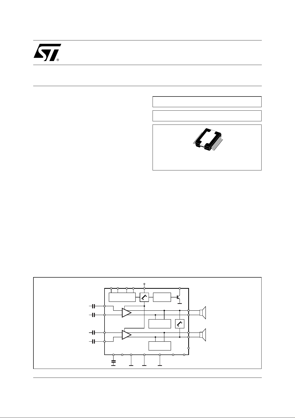
The TDA7575 is a new BCD technology DUAL
BRIDGE type of car radio amplifier in PowerSO36
package specially i ntended for car radio applicati ons.
Ω,
1x150W/1
Ω
TDA7575
MULTIPOWER BCD TECHNOLOGY
MOSFET OUTPUT POWER STAGE
PowerSO36 (Slug up)
ORDERING NUMBER: TDA7575
Thanks to the DMOS output stage the TDA7575 has
a very low distortion allowing a clear powerful sound.
Among the features, its superior efficiency performance coming from the internal exclusive structure,
makes it the most suitabl e devic e to si mplify the ther mal management in high power sets.The dissipated
output power under average listening condition is in
fact reduced up to 50% when compared to the level
provided by conventional class AB solutions.
This device is equipped with a full diagnostic array
that communicates the status of each speaker
through the I
bility of driving loads down to 1
into a single channel. It is also possible to disable the
I2C and co ntrol the TDA7 575 by mean s of t he u sual STBY and MUTE pins.
2
C bus.
The TDA7575 has al so the possi-
Ω
paralleling the outputs
BLOCK DIAGRAM
V
ADDRESS
A B CLK
I2CBUS
IN1+
IN1-
IN2+
IN2-
SVR S_GND
ST-BY/HE 1Ω MUTE
October 2002
This is preliminary information on a new product now in development. Details are subject to change without notice.
S
DAT A VCC CD_OUT
CLIP
DETECTOR
SHORT CIRCUIT
PROTECTION
SHORT CIRCUIT
PROTECTION
PW_GND TAB
OUT1+
OUT1-
OUT2+
OUT2-
2
C EN
I
D01AU1269
1/17
Page 2
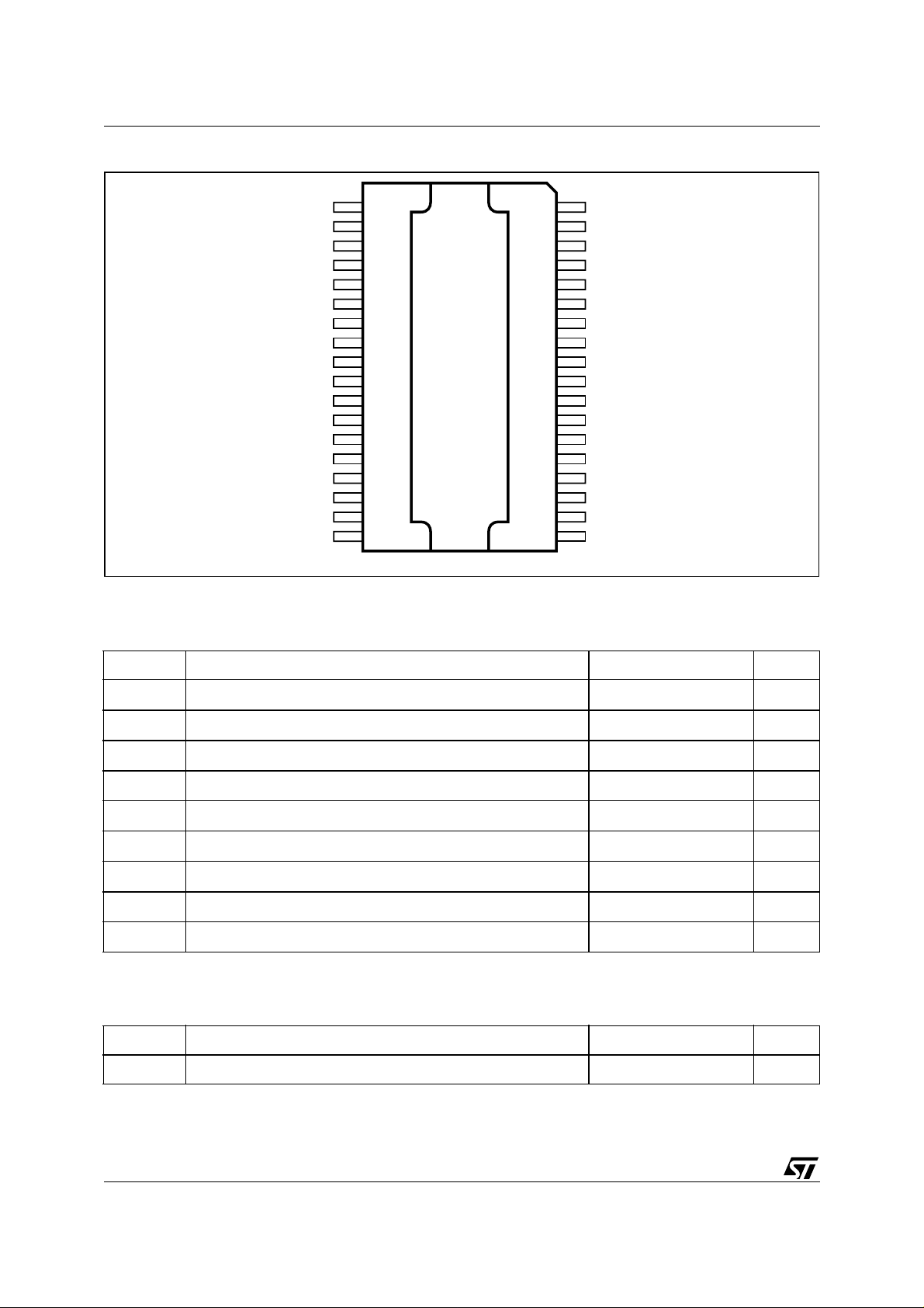
TDA7575
PIN CONNECTION
(Top view)
OUT1+
OUT1+
PWGND
PWGND
PWGND
PWGND
OUT2+
OUT2+
VCC
VCC
OUT1OUT1OUT2OUT2-
VCC
VCC
36
35
34
33
B
A
32
31
30
29
28
26
25
23
22
21
20
19
D01AU1270
1
2
3
4
5
6
7
8
9
1027
11
12
1324
14
15
16
17
18
TAB
IN1+
IN1MUTE
ST_BY
SGND
DATA
CK
N.C.
N.C.
N.C.
N.C.
SVR
CD-OUT
1-OHM
I2C-EN
IN2IN2+
ABSOLUTE MAXIMUM RATINGS
Symbol Parameter Value Unit
V
op
V
V
peak
V
CK
V
DA TA
I
O
I
O
P
tot
T
stg
Operating Supply Voltage 18 V
DC Supply Voltage 28 V
S
Peak Supply Voltage (for t = 50ms) 50 V
CK pin Voltage 6 V
Data Pin Voltage 6 V
Output Peak Current (not repetitive t = 100ms) 8 A
Output Peak Current (repetitive f > 10Hz) 6 A
Power Dissipation T
= 70°C 86 W
case
, TjStorage and Junction Temperature -55 to 150 °C
THERMAL DATA
Symbol Parameter Value Unit
Rth j-case Thermal Resistance Junction-case Max 1 °C/W
2/17
Page 3
TDA7575
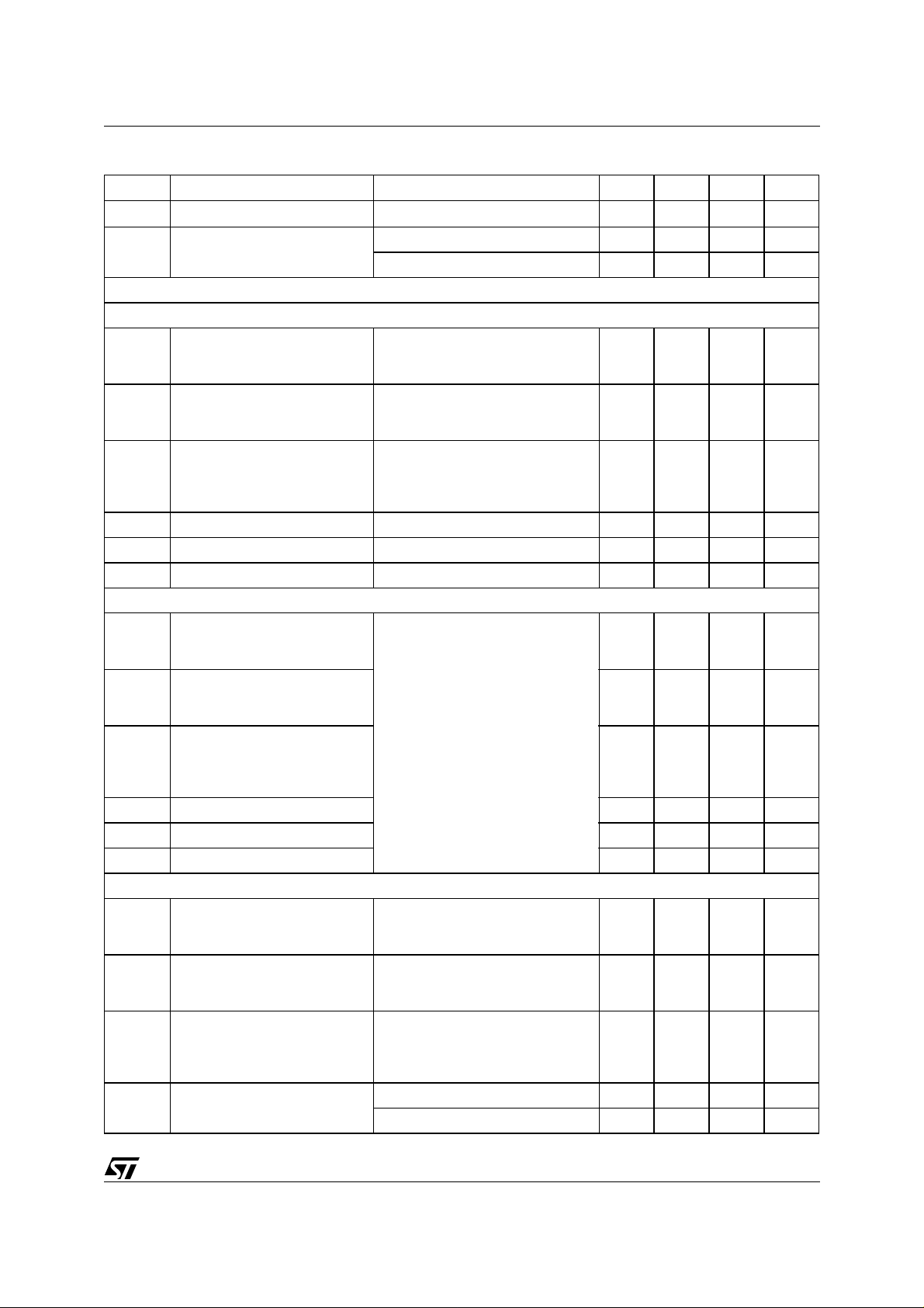
ELECTRICAL CHARACTERISTCS:
(VS=14.4V; f=1KHz; RL=4Ω; Tamb= 25°C unless otherwise specified)
Symbol Parameter Test Condition Min. Typ. Max. Unit
POWER AMPLIFIER
V
Po Output Power EIAJ (V
Supply Voltage Range 8 18 V
S
I
Total Quiescent Drain Current 50 130 200 mA
d
= 13.7V) 35 40 W
S
THD = 10%
THD = 1%; BTL MODE
RL = 2Ω; EIAJ (VS = 13.7V)
RL = 2Ω; THD 10%
RL = 2Ω; THD 1%
RL = 2Ω; MAX POWER
25 28
22
60
45
65
50
37
70
75
Single channel configuration
= 1Ω;
L
= 4-8W
O
= 1; PO = 4-30W
L
125
80
140
130
84
150
0.03
0.03
0.1
0.1
0.5
0.02 0.1 %
40 60 µV
THD Total Harmonic Distortion P
C
R
G
∆G
G
∆G
E
Cross Talk Rg = 600Ω; PO = 1W 60 75 dB
T
Input Impedance 60 100 13 0 KΩ
IN
Voltage Gain 1 (default) 25 26 27 dB
V1
Voltage Gain Match 1 -1 0 1 dB
V1
Voltage Gain 2 11 12 13 dB
V2
Voltage Gain Match 2 -1 0 1 dB
V2
Output Noise Voltage Gain 1 Rg = 600Ω; Gv = 26dB
IN1
(1Ω pin >2.5V); R
EIAJ (VS = 13.7V)
THD 3%
MAX POWER
= 1-12W; STD MODE
O
HE MODE; PO = 1-2W
HE MODE; P
= 1-12W, f = 10kHz 0.15 0.5 %
P
O
R
= 2; HE MODE; Po = 3W 0.03 0.5 %
L
Single channel configuration
(1Ω pin >2.5V); R
filter 20 to 22kHz
E
Output Noise Voltage Gain 2 Rg = 600Ω; Gv = 12dB
IN2
15 25 µV
filter 20 to 22kHz
SVR Supply Voltage Rejection f = 100Hz to 10kHz; V
= 1Vpk;
r
50 60 dB
Rg = 600Ω
W
W
W
W
W
W
W
W
W
%
%
%
BW Power Bandwidth (-3dB) 100 KHz
A
I
A
V
V
CMRR Input CMRR V
Stand-by Attenuation 90 100 dB
SB
Stand-by Current Consumption 2 20 µA
SB
Mute Attenuation 80 90 dB
M
Offset Voltage Mute & Play -100 0 100 mV
OS
Min. Supply Mute Threshold 7 7.5 8 V
AM
= 1Vpk-pk; Rg = 0 Ω 50 60 dB
CM
3/17
Page 4
TDA7575
ELECTRICAL CHARACTERISTCS:
(continued)
Symbol Parameter Test Condition Min. Typ. Max. Unit
V
Maximum common mode input
MC
f = 1kHz 1 Vrms
level
SR Slew Rate 1.5 4 V/µs
∆V
∆V
T
T
V
V
V
V
V
V
V
I2C I2C pin current (stby) 0V < I2C EN < 18V, V
I2C I2C pin current (operative) I2C EN <18V, V
V
1OHM
V
1OHM
Mute/Unmute Transient A-weighted -100 0 10 0 mVpp
PM
Mute/Stand-by Transient A-weighted -100 0 100 mVpp
TO
Turn on Delay D2 (IB1) 0 to 1 15 40 ms
ON
Turn off Delay D2 (IB1) 1 to 0 15 40 ms
OFF
St-By pin for St-By 0 1.5 V
OFF
St-By pin for standard bridge 3.5 5 V
SB
St-By pin for Hi-eff 7 1 8 V
HE
I
St-By pin Current 1.5 < V
O
St-By Pin Current V
Mute pin voltage for mute mode 0 1.5 V
m
Mute pin voltage for play mode 3.5 18 V
m
I
Mute pin current (ST_BY) V
m
I
Mute pin current (operative) 0V < V
m
I2C pin voltage for I2C disabled 0 1.5 V
I2C
I2C pin voltage for I2C enabled 2.5 18 V
I2C
< 1.5V -10 0 10 µA
stby
= 0V, V
mute
< 18V 7 160 200 µA
stby/HE
< 1.5V -5 0 5 µA
stby
mute
< 18V, V
> 3.5V 65 100 µA
stby
< 1.5V -5 0 5 µA
stby
>3.5V 7 11 15 µA
stby
1OHM pin voltage for 2ch mode 0 1.5 V
1OHM pin voltage for 1ohm
2.5 18 V
mode
I
1OHM
I
1OHM
1OHM pin current (stby) 0V < 1OHM <18V, V
1OHM pin current (operative) 1OHM <18V, V
stby
< 1.5V -5 0 5 µA
stby
> 3.5V 7 11 15 µA
La A Pin Voltage Low logic level 0 1.5 V
Ha High logic level 2.5 18 V
Ia A Pin Current (ST-BY) 0V < A < 18V, V
Ia A Pin Current (Operative) A<18V, V
stby
< 1.5V -5 0 5 µA
stby
> 3.5V 7 11 15 µA
Lb B Pin Voltage Low logic level 0 1.5 V
Hb High logic level 2.5 18 V
Ib B Pin Current (ST-BY) 0V < B < 18V, V
Ib B Pin Current (Operative) B < 18V, V
T
T
I
CDH
Thermal warning 150 °C
W
Thermal Protection intervention 170 °C
PI
Clip Pin High Leakage Current CD off, 0V < VCD < 5.5V -15 0 15 µA
stby
< 1.5V -5 0 5 µA
stby
> 3.5V 7 11 15 µA
4/17
Page 5
TDA7575
ELECTRICAL CHARACTERISTCS:
(continued)
Symbol Parameter Test Condition Min. Typ. Max. Unit
I
CDL
Clip Pin Low Sink Current CD on; VCD < 300mV 1 mA
CD Clip detect THD level D0 (IB1) = 0 0.8 1.3 2.5 %
D0 (IB1) = 1 5 10 15 %
(*) ST-BY Pin high enables I2C bus; ST-BY Pin low puts the device in ST-BY condition.(see “prog” for more details)
TURN ON DIAGNOSTICS
Pgnd Short to GND det. (below this
(Power Amplifier Mode)
Power Amplifier in st-by condition 1.2 V
limit, the Output is considered in
Short Circuit to GND)
Pvs Short to Vs det. (above this
V
-0.9 V
s
limit, the Output is considered in
Short Circuit to VS)
Pnop Normal operation
1.8 V
-1.5 V
s
thresholds.(Within these limits,
the Output is considered
without faults).
Lsc Shorted Load det. 0.5 Ω
Lop Open Load det. 130 Ω
Lnop Normal Load det. 1.5 70 Ω
TURN ON DIAGNOSTICS
Pgnd Short to GND det. (below this
(Line Driver Mode)
Power Amplifier in st-by 1.2 V
limit, the Output is considered in
Short Circuit to GND)
Pvs Short to Vs det. (above this
-0.9 V
V
s
limit, the Output is considered in
Short Circuit to VS)
Pnop Normal operation
1.8 V
-1.5 V
s
thresholds.(Within these limits,
the Output is considered
without faults).
Lsc Shorted Load det. 1.5 Ω
Lop Open Load det. 400 Ω
Lnop Normal Load det. 4.5 200 Ω
PERMANENT DIAGNOSTICS
Pgnd Short to GND det. (below this
limit, the Output is considered in
Short Circuit to GND)
Pvs Short to Vs det. (above this
(Power Amplifier Mode or Line Driver Mode)
Power Amplifier in Mute or Play
condition, one or more short circuits
protection activated
1.2 V
Vs - 0.9
limit, the Output is considered in
Short Circuit to VS)
Pnop Normal operation
1.8 V
-1.5 V
s
thresholds.(Within these limits,
the Output is considered
without faults).
Lsc Shorted Load det. Pow. Amp. mode 0.5 Ω
Line Driver mode 1.5 Ω
V
5/17
Page 6

TDA7575
ELECTRICAL CHARACTERISTCS:
Symbol Parameter Test Condition Min. Typ. Max. Unit
V
2
C BUS INTERFACE
I
f
SCL
V
V
Offset Detection Power Amplifier in play condition
O
Clock Frequency 400 KHz
Input Low Voltage 1.5 V
IL
Input High Voltage 2.3 V
IH
(continued)
±1.5 ±2 ±2.5 V
AC Input signals = 0
I2C BUS INTERFACE
Data transm ission f rom mic roproc esso r to the TDA7575 an d viceve rsa take s place t hr ough the 2 wi res I2C BUS interface, consisting of the two lines SDA and SCL (pull-up resistors to positi ve supply voltage must be connected).
Data Validity
As shown by fig. 1, the data on the SDA line must be stable during the high period of the clock.
The HIGH and LOW state of the data line can only change when the clock signal on the SCL line is LOW.
Start and Stop Conditions
As shown by fig. 2 a start condition is a HIGH to LOW transition of the SDA line while SCL is HIGH.
The stop condition is a LOW to HIGH transition of the SDA line while SCL is HIGH.
Byte Format
Every byte transferred to the SDA line must contain 8 bits. Each byte must be followed by an acknowledge bit.
The MSB is transferred first.
Acknowledge
The transmitter* puts a resistive HIGH level on the SDA line during the acknowledge c lock pulse ( see fig.3). The
receiver** the acknowledges has to pull- down (LOW) the SDA line during the acknowledge cloc k pulse, so that
the SDAline is stable LOW during this clock pulse.
* Transmitter
= master (
= slave (TDA7575) when the
µ
P) when it writes an address to the TDA7575
µ
P reads a data byte from TDA7575
** Receiv er
= slave (TDA7575) when the
µ
P writes an address to the TDA7575
= master (mP) when it reads a data byte from TDA7575
6/17
Page 7

Figure 1. Dat a Va li di t y on t he I2CBUS
SDA
SCL
TDA7575
DATA LINE
STABLE, DATA
Figure 2. Timin g D i agramon the I
SCL
SDA
START
Figure 3.
VALID
2
CBUS
CHANGE
DATA
ALLOWED
D99AU1032
D99AU1031
2
I
STOP
CBUS
SCL
SDA
START
1
MSB
23789
D99AU1033
ACKNOWLEDGMENT
FROM RECEIVER
1 Ohm Capability Setting
It is possible to drive 1OHM load paralleling the outputs into a single channel.
In order to implement this feature, outputs are to be connected on the board as follows:
OUT1+ (PIN35 and PIN36) shorted to OUT2+ (PIN19 and PIN20)
OUT1- (PIN28 and PIN29) shorted to OUT2- (PIN26 and PIN27).
7/17
Page 8

TDA7575
It is recommended to minimize the impedance on the board betw een OUT2 and the load in order to minimize
THD distortion. It is also recommended to control the maximum mismatch impedance between VCC pins
(PIN21/PIN22 respect to PIN33/PIN34) and between PWGND pins (PIN24/PIN25 respect to PIN30/PIN31),
mismatch that must not exceed a value of 20 mOhm.
With 1OHM feature settled the active input is IN2 (PIN17 and PIN18), therefore IN1 pins should be let floating.
It is possible to set the load capability acting on 1OHM pin as follows:
1OHM PIN (PIN15) < 1.5V: two channels mode (for a minimum load of 2 OHM)
1OHM PIN (PIN15) > 2.5V: one channel mode (for 1 OHM load).
IT IS TO REMEMBER THAT 1 0HM FUNCTION IS A HARDWARE SELECTION.
Therefore it is recommended to leave 1OHM PIN fl oating or shorted to G ND to set the two channels mode con-
figuration, or to short 1OHM PIN to VCC to set the one channel (1OHM) configuration.
I2C Abilitation Setting
It is possible to disable the I2C interface by acting on I2C PIN (PIN16) and contr ol the TDA7575 by means of the
usual ST-BY and MUTE pins. In order to activate or deactivate this feature, I
2
I2C PIN (PIN16) < 1.5V: I
I2C PIN (PIN16) > 2.5V: I
It is also possible to let I
C bus interface deactivated
2
C bus interface activated
2
C PIN floating to deactivate the I2C bus interface, or to short I2C PIN to VCC to activate
it.
C PIN must be set as follows:
2
In particular:
2
C ENABLED: I2C pin (PIN16) > 2.5V
I
– STD MODE: Vstby (PIN5) > 3.5V, IB2 (D1)=0
– HE MODE: Vstby (PIN5) > 3.5V, IB2(D1)=1
– PLAY MODE: Vmute (pin 4) >3.5V, IB1 (D2) = 1
The amplifier can always be sw itched off by putting Vstby to 0V, but with I2C enabled it can be turn on only
through I
2
C DISABLED: I2C pin (PIN16) < 1.5V
I
2
C (with Vstby > 3.5V).
– STD MODE: 3.5V < stby (PIN5) < 5
– HE MODE : Vstby ( PIN5 ) > 7 V
– PLAY MODE: Vmute (pin 4) >3.5V
For both STD and HE MODE the play/mute mode can be set acting on Vmute pin.
8/17
Page 9

SOFTWARE SPECIFICATIONS
All the functions of the TDA7575 are activated by I2C interface.
The bit 0 of the "ADDRESS BYTE" defines if the next bytes are write instruction (fr o m
instruction (from TDA7575 to
µ
P).
ADDRESS SELECTION
A6
A5
A4
A3
A2
A1
A0
R/W
1
1
0
1
0
B
A
X
If R/W = 0, the µP sends 2 "Instruction Bytes": IB1 and IB2.
IB1
D7
D6
D5
D4
D3
D2
D1
D0
X
Diagnostic enable (D6 = 1)
Diagnostic defeat (D6 = 0)
Offset Detection enable (D5 = 1)
Offset Detection defeat (D5 = 0)
Gain = 26dB (D4 = 0)
Gain = 12dB (D4 = 1)
X
Mute (D2 = 0)
Unmute (D2 = 1)
X
CD 2% (D0 = 0)
CD 10% (D0 = 1)
TDA7575
µ
P to TDA7575) or read
IB2
D7
D6
D5
D4
D3
D2
D1
D0
X
used for testing
used for testing
Stand-by on - Amplifier not working - (D4 = 0)
Stand-by off - Amplifier working - (D4 = 1)
Power Amplifier Mode Diagnostic (D3 = 0);
Line Driver Mode Diagnostic (D3 = 1)
X
Power amplifier working in standard mode (D1 = 0)
Power amplifier working in high efficiency mode (D1 = 1)
X
9/17
Page 10

TDA7575
If R/W = 1, the TDA7575 sends 2 "Diagnostics Bytes" to µP: DB1 and DB2.
DB1
D7
Thermal warming (if Tchip ≥ 150°C, D7 = 1)
DB2
D6
D5
D4
D3
D2
D1
D0
D7
Diag. cycle not activated or not terminated (D6 = 0)
Diag. cycle terminated (D6 = 1)
X
Channel 1
Turn-on diagnostic (D4 = 0)
Permanent diagnostic (D4 = 1)
Channel 1
Normal load (D3 = 0)
Short load (D3 = 1)
Channel 1
Turn-on diag.: No open load (D2 = 0)
Offset diag.: No output offset (D2 = 0)
Channel 1
No short to V
Short to Vcc (D1 = 1)
Channel 1
No short to GND (D1 = 0)
Short to GND (D1 = 1)
Offset detection not activated (D7 = 0)
Offset detection activated (D7 = 1)
Open load detection (D2 = 1)
Output offset detection (D2 = 1)
(D1 = 0)
cc
10/17
D6
D5
D4
D3
D2
D1
D0
X
X
Channel 2
Turn-on diagnostic (D4 = 0)
Permanent diagnostic (D4 = 1)
Channel 2
Normal load (D3 = 0)
Short load (D3 = 1)
Channel 2
Turn-on diag.: No open load (D2 = 0)
Permanent diag.: No output offset (D2 = 0)
Channel 2
No short to V
Short to V
Channel 2
No short to GND (D1 = 0)
Short to GND (D1 = 1)
Open load detection (D2 = 1)
Output offset detection (D2 = 1)
(D1 = 0)
cc
(D1 = 1)
cc
Page 11

TDA7575
Examples of bytes sequence
1
- Turn-On diagnostic - Write operation
Start Address byte with D0 = 0 ACK IB1 with D6 = 1 ACK IB2 ACK STOP
2
- Turn-On diagnostic - Read operation
Start Address byte with D0 = 1 ACK DB1 ACK DB2 ACK STOP
The delay from 1 to 2 can be selected by software, starting from T.B.D. ms
3a
- Turn-On of the power amplifier with mute on, diagnostic defeat.
Start Address byte with D0 = 0 ACK IB1 ACK IB2 ACK STOP
X000XXXX XXX1XX1X
3b
- Turn-Off of the power amplifier
Start Address byte with D0 = 0 ACK IB1 ACK IB2 ACK STOP
X0XXXXXX XXX0XXXX
4
- Offset detection procedure enable
Start Address byte with D0 = 0 ACK IB1 ACK IB2 ACK STOP
XX1XX1XX XXX1XXXX
5
- Offset detection procedure stop and reading operation (the results are valid only for the offset detection bits
(D2 of the bytes DB1, DB2, DB3, DB4).
Start Address byte with D0 = 1 ACK DB1 ACK DB2 ACK STOP
■
The purpose of this test is to check i f a D.C. offset (2V typ.) is present on the outputs, produced by input
capacitor with anomalous leackage current or humidity between pins.
■
The delay from 4 to 5 can be selected by software, starting from T.B.D. ms
DIAGNO STICS FUNCTIO NAL DESCRIPTION:
a) TURN-ON DIAGNOSTIC.
It is activated at the turn-on (stand-by out) under I2C bus request. Detectable output faults are:
–SHORT TO GND
–SHORT TO Vs
– SHORT ACROSS THE SPEAKER
– OPEN SPEAKER
To verify if any of the above misconnections are in plac e, a subsonic (inaudi ble) current pulse (fig. A ) is internall y
generated, sent through the speaker(s) and su nk back.The Tur n On diagnostic s t atus is i nternally sto red unti l a
successive diagnostic pulse is requested (after a I2C reading).
If the "stand-by ou t" and "diag. ena ble" c ommands ar e both given through a single programming step, the pulse
takes place first (power stage still in stand-by mode, low, outputs= high impedance).
11/17
Page 12

TDA7575
Afterwards, when the Amplifier i s bi ased, the P ERMANENT diagnostic takes plac e. The prev ious Turn On state
is kept until a short appears at the outputs.
Fig A: Turn - On diagnostic:
working principle
Vs~5V
Isource
CH+
I (mA)
Isource
Isink
CH-
Isink
~100mS
t (ms)
Measure time
Fig. B and C show SVR and OUTPUT waveforms at the turn-on (stand-by out) with and without TURN-ON DIAGNOSTIC.
Fig B: SVR and Output behaviour
CASE 1:
without turn-on diagnostic
Vsvr
Out
Permanent diagnostic
acquisition time (100mS Typ)
Bias (power amp turn-on)
I2CB DATA
FIG. C: SVR and Output pin behaviour
CASE 2:
with turn-on diagnostic
Vsvr
Out
I2CB D AT A
acquisit i on tim e ( 100mS Typ)
Diagnostic Enable
(Turn-on)
Turn-on diagnost ic
Bias (power am p tu r n-o n)
permitted time
Diagnostic Enable
(Permanent)
Permanent Diagnostics data (output)
Turn-on Diagnost i cs data (output)
permitted time
FAULT
event
Read Data
permitted time
Diagnostic Enable
(Permanent)
t
Read Data
Permane nt diagnostic
acquisit i on tim e (100mS Typ)
FAULT
event
Perman ent Dia gnost ics data (output)
permitted time
t
12/17
Page 13

TDA7575
The information related to the outputs status is read and memorized at the end of the current pulse top. The
acquisition time is 100 ms (typ.). No audibl e noise is generated in the process . As for SHORT TO GND / Vs the
fault-detection thresholds remain unchanged from 26 dB to 12 dB gain setting. They are as follows:
S.C. to GND x S.C. to Vs
0V 1.8V VS-1.5V V
1.2V VS-0.9V
xNormal Operation
D02AU1341
S
Concerning SHORT ACROSS THE SPEAKER / OPEN SPEAKER, the threshold varies from 26 dB to 12 dB
gain setting, since different loads are expected (either normal speaker's impedance or high impedance). The
values in case of 26 dB gain are as follows:
S.C. across Load x Open Load
0V 1.5Ω 70Ω Infinite
0.5Ω
xNormal Operation
130Ω
D01AU1254
If the Line-Driver mode (Gv= 12 dB and Line Driver Mode diagnostic = 1) is selected, the same thresholds will
change as follows:
S.C. across Load x Open Load
0Ω 4.5Ω 200Ω infinite
1.5Ω 400Ω
xNormal Operation
D01AU1252
b) PERMANENT DIAGNOSTICS
.
Detectable conventional faults are:
–SHORT TO GND
–SHORT TO Vs
– SHORT ACROSS THE SPEAKER
The following additional features are provided:
– OUTPUT OFFSET DETECTION
The TDA7575 has 2 operating statuses:
1) RESTART mode. The diagnostic is not enabled. Each audio channel oper ates independe ntly from each other. If any of the a.m. faults occurs, only the channel(s) interested is shut down. A check of the output status is
made every 1 ms (fig. G). Restart takes place when the overload is removed.
2) DIAGNOSTIC mode. It is enabled via I
2
C bus and self activates if an output overload (such to cause the intervention of the short-circuit protection) occurs to the speakers outputs . Once activated, the diagnostics procedure develops as follows (fig. H):
– To avoid momentary re-circulation spikes from giving erroneous diagnostics, a check of the output
status is made after 1ms: if normal situation (no overloads) is detected, the diagnostic is not performed and the channel returns back active.
– Instead, if an overload is det ected during the c heck afte r 1 m s, then a diagnostic cycle having a du-
ration of about 100 ms is started.
– After a diagnostic cycle, the audio channel interested by the fault is switched to RESTART mode. The
13/17
Page 14

TDA7575
relevant data are stored inside the device and can be read by the m icroprocessor. When one cycle
has terminated, the next one is activated by an I
2
C reading. This is to ensure continuous diagnostics
throughout the car-radio operating time.
– To check the status of the device a sampling system is needed. The timing is chosen at microproces-
sor level (over than half a second is recommended).
Fig. G: Restart timing without Diagnostic Enable (Permanent)
Each 1mS time, a sampling of the fault is done
Out
1mS
t
Short circuit removed
Overcurrent and short
circuit protection intervention
(i.e. short circuit to GND)
1-2mS
1mS 1mS 1mS
Fig H: Restart timing with Diagnostic Enable (Permanent)
1mS 100mS 1mS1mS
t
Overcurrent and short
circuit protection intervention
(i.e. short c ircuit to GND)
Short circuit removed
OUTPUT DC OFFSET DETECTION.
Any DC output offset exceeding +/- 2 V are signalled out. This inconvenient might occur as a consequence of
initially defective or aged and worn-out input capacitors feeding a DC component to the inputs, so putting the
speakers at risk of overheating.
This diagnostic has to be performed with low-level output AC signal (or Vin = 0).
The test is run with selectable time duration by microprocessor (from a "start" to a "stop" command):
– START = Last reading operation or setting IB1 - D5 - (OFFSET enable) to 1
– STOP = Actual reading operation
Excess offset is signalled out if persistent throughout the assigned testing time. This feature is disabled if any
overloads leading to activation of the short-circuit protection occurs in the process.
14/17
Page 15

TDA7575
MULTIPLE FAULTS.
When more misconnections are simultaneously in place at the audio outputs, it is guaranteed that at least one
of them is initially read out. The others are notified after successive cycles of I
provided that the diagnostic is enabled. This is true for both kinds of diagnostic (Turn on and Permanent).
The table below shows all the coupl es of double-fault po ssible. It sh ould be taken into account that a shor t circuit
with the 4 ohm speaker unconnected is considered as double fault.
Double fault table for Turn On Diagnostic
S. GND (sc) S. GND (sk) S. Vs S. Across L. Open L.
S. GND (sc)
S. GND (sk)
S. Vs
S. Across L.
Open L.
S. GND S. GND S. Vs + S. GND S. GND S. GND
/ S. GND S. Vs S. GND Open L. (*)
/ / S. Vs S. Vs S. Vs
/ / / S. Across L. N.A.
/ / / / Open L. (*)
S. GND (so) / S. GND (sk) in the above table make a distinction according to which of the 2 outputs is shorted
to ground (test-current source side= so, test-current sink side = sk). More precisely, in both the Channels SO =
CH+, and SK = CH-.
In Permanent Diagnostic the table is the same, with only a difference concerning Open Load(*) , which is not
among the recognisable faults. Should an Open Load be present during the device's normal working, it would
be detected at a subsequent Turn on Diagnostic cycle (i.e. at the successive Car Radio Turn on).
2
C reading and faults removal,
FAULTS AVAILABILITY
All the resul ts c oming from I2Cbus, by read operati ons, are the cons equence of measurements inside a defined
period of time. If the fault is stable throughout the whole period, it will be sent out. This is true for DC diagnostic
(Turn on and Permanent), for Offset Detector.
To guarantee always resident functions, every kind of diagnostic cycles (Turn on, Permanent, Offset) will be
reactivate after any I2C reading operation. So, when the micro reads the I
2
C, a new cycle will be able to start,
but the read data will come from the previ ous diag. cycle (i.e . The device i s in Turn On state, with a short to Gnd,
then the short is removed and mi cr o reads I2C . The short to Gnd is sti ll present in bytes, because it is the result
of the previous cycle. If another I2C reading operation occurs, the bytes do not show the short). In general to
observe a change in Diagnostic bytes, two I2C reading operations are necessary.
I2C PROGRAMMING/READING SEQUENCES
A correct turn on/off sequenc e respectful of the diagnostic timings and producing no audible noises could be as
follows (after battery connection):
– TURN-ON: (STAND-BY OUT + DIAG ENABLE) --- 500 ms (min) --- MUTING OUT
– TURN-OFF: MUTING IN --- 20 ms --- (DIAG DISABLE + STAND-BY IN)
Car Radio Installation: DIAG ENABLE (write) --- 200 ms --- I2C read (repeat until All faults disappear).
– OFFSET TEST: Device in Play (no signal) --
2
– OFFSET ENABLE - 30ms - I
C reading
(repeat I2C reading until high-offset message disappears).
15/17
Page 16

TDA7575
DIM.
(1) “D and E1” do not include mold flash or protusions.
(2) No intrusion allowed inwards the leads.
MIN. TYP. MAX. MIN. TYP. MAX.
A 3.25 3.5 0.128 0.138
A2 3.3 0.13
A4 0.8 1 0.031 0.039
A5 0.2 0.008
a1 0 0.075 0 0.003
b 0.22 0.38 0.008 0.015
c 0.23 0.32 0.009 0.012
D 15.8 16 0.622 0.6 30
D1 9.4 9.8 0.37 0.38
D2 1 0.039
E 13.9 14.5 0.547 0.57
E1 1 0.9 11.1 0.429 0.437
E2 2.9 0.114
E3 5.8 6.2 0.228 0.244
E4 2.9 3.2 0.114 1.259
e
e3 11.05 0.435
G 0 0.075 0 0.003
H 15.5 15.9 0.61 0.625
h 1.1 0.043
L 0.8 1.1 0.031 0.043
N 10˚ (max)
s 8˚ (max)
Mold flash or protusions shall not exce ed 0.15mm (0.006”)
mm inch
0.65 0.026
OUTLINE AND
MECHANICAL DA TA
PowerSO36 (SLUG UP)
16/17
7183931
Page 17

TDA7575
Information furnished is believed to be accurate and reliable. However, STMicroelectronics assumes no responsibility for the consequences
of use of such information nor for any infringement of patents or other rights of third parties which may result from its use. No license is granted
by implic ation or otherwise under any patent or p atent right s of STMicroelectr oni cs. Spec i fications mentioned i n this publication are subje ct
to change without notice. This publication supersedes and replaces all information previously supplied. STMicroelectronics products are not
authorized for use as cri tical comp onents in life support dev i ces or systems wi thout express written approval of STMicroe l ectronics.
The ST logo is a registered trademark of STMicroelectronics
2002 STMi croelectronics - All Ri ghts Rese rved
Australia - Brazil - Canada - China - Finla nd - France - G erm any - Hong K ong - India - Israel - Italy - J apan -Malaysia - Malta - Morocco -
Singap ore - Spain - Sw eden - Switze rl and - Unit ed K i ngdom - United States .
STMicroelectronics GROUP OF COMPANIES
http://www.s t. com
17/17
 Loading...