

Page 1

®
y
q
DIGITAL AM/FM SIGNAL PROCESSOR
FULL SOFTWARE FLEXIBILITY WITH TWO
24X24 BIT DSP CORES
AM/FM PROCESSING
AUDIO-PROCESSING AND SOUND-PROC-
ESSING
HARDWARE RDS FILTER, DEMODULATOR
& DECODER
INTEGRATED CODEC
IIC AND SPI CONTROL INTERFACES
SPI DEDICATED TO DISPLAY MICRO
6 CHANNEL SERIAL AUDIO INTERFACE SAI
SPDIF RECEIVER WITH SAMPLE RATE
CONVERTER
EXTERNAL MEMORY INTERFACE
DOUBLE DEBUG INTERFACE
ON-CHIP PLL
5V-TOLERANT 3V I/O INTERFACE
MULTIFUNCTION GENERAL PURPOSE I/O PORTS
TDA7500
PRODUCT PREVIEW
TQFP100 Power with Slug Down
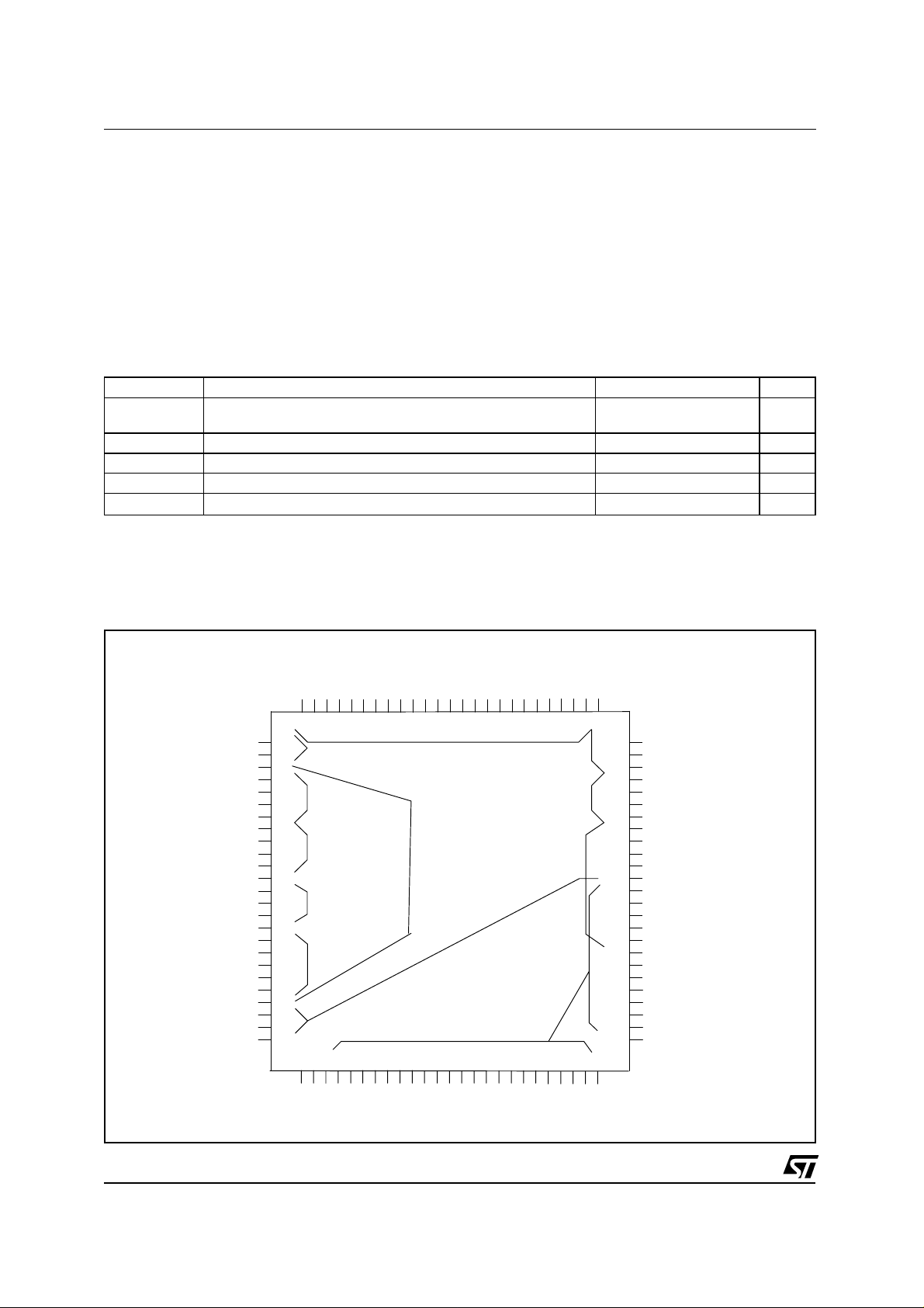
DESCRIPTION
The TDA7500 is an integrated circuit implementing a fully digital, integrated and advanced solution to perform the signal processing in front of
the power amplifier and behind the AM/FM tuner
or any other audio sources. The chip integrates
two 43 MIPs DSP cores: one for stereo decoding,
noise blanking, weak signal processing and multi-
BLOCK DIAGRAM
analog audio in
AM-IF
CC
CD
tel,navi
AM/FM lev.
AM/FM mpx
RDS mpx
uP control
Main micro
Display uP
Spectrum Analyser
CLK in
8.55MHz
Data, ctl
128k (4M) x 8
(1 I/O)
Address
Audio Bus 6 ch.
dig. aud. out
clkt, wst, clkr, wsr
dig. aud. in
CD input
CDC input
MD input
RDS bit/blk Int.
RDS
Error corrected RDS blocks
alternativel
RDS clk, dat,
1
2
3
4
2
3
1
(4 I/O's)
(4 I/O's)
Audio Bus Synch.
8+3
(2 I/O's)
(2 I/O's)
(1 I/O)
(4 I/O's)
:
ual, ARI
4
4
17
3
4
2
4
4
RDS
Mute
Input Multiplexer,
Analog Level Adjus t
Σ∆
Modulator
Σ∆
Modulator
Σ∆
Modulat or
Σ∆
Modulat or
IIC / SPI
SPI
XTAL Osc.,
PLL
Ext. Memory
Interface
Serial A u d io
Interface
SPDIF
Interface
Mux
Grp & blk
sync., error
SPI
correction
supply
Cref
2
2
AM
Noise
Detector
VDD GND
32
Decimation
Filter
Decimation
Filter
1 stereo channel
Sample Rate
Converter
Demod.
2 channel analog bypass
Exchange
Interface
RDS
Filter
3
IIC
CODEC-ref
Voltage
Ref.
Codec
Ctl Reg.
Test I/F
DSP Orpheus Core
including 12 GPIO•s including 12 GPIO•s
FM processing,
AM proc es sing ,
Traffic mem., Dolby,
Speech synth., etc...
Debug, Test Interface
Oversampling
Filter
Oversampling
Filter
Oversampling
Filter
X Register
Ram 512
Y Register
Ram 512
Program
Ram 1024
Rom 256
DSP1
VS SigGnd
Output
Analog Volume Co nt rol,
select.
Line Drive r
Noise
Shaper
Noise
Shaper
Noise
Shaper
X bus 0X bus 1
DSP Orpheus Core
Audi o processing ,
Sound pro c es s ing
Debug, Test Interface
DSP0
X Register
Ram 512
Y Register
Ram 512
Program
Ram 5632
Rom 256
RefOut
DAC-ref
SC Filter
SC Filter
SC Filter
SC Filter
SC Filter
SC Filter
6
6
5
5
2
4
4
signal/line out
Int
Reset
VDD
GND
Test
(3 I/O's)
(3 I/O's)
September 1999
1/14
This is preliminary information on a new product foreseen to be developed. Details are subject to change without notice.
Page 2
y
g
TDA7500
path detection and one for sound processing. An
I2C/SPI interface is implemented for control and
communication with the main micro.
A separate SPI is available to interface the display micro.
The DSP cores are integrated with their associated data and program memories. The peripherals and interfaces I
2
C, SPI, Serial Audio Interface
(SAI), PLL Oscillator, External Memory Interface,
(EMI), General Purpose I/O register (Port A) and
by DSP0, whereas the A/D registers, the SPDIF
and the General Purpose I/O register (Port B) are
connected to and controlled by DSP1. The Debug
and Test Interface are connected to both DSP
cores.
The TDA7500 is supposed to be used in kit with
the TDA7501 or any other device of the same
family. Thanks to the serial audio interface also
digital sources can be processed and a direct
output to a digital bus is also available.
the D/A registers are connected to and controlled
ABSOLUTE MAXIMUM RATINGS
Symbol Parameter Value Unit
VDD
VCC
Power supplies Digital
Analog
4.6
4.6
Analog Input Voltage -0.5 to (VDD+0.5) V
Digital Input Voltage -0.5 to (VCC+0.5) V
T
amb
T
stg
Warning: Operation at or beyond these limit may result in permanent damage to the device.
Normal operation is not guaranteed at these extremes.
Operating Temperature Range -40 to 85 °C
Storage Temperature -55 to 150 °C
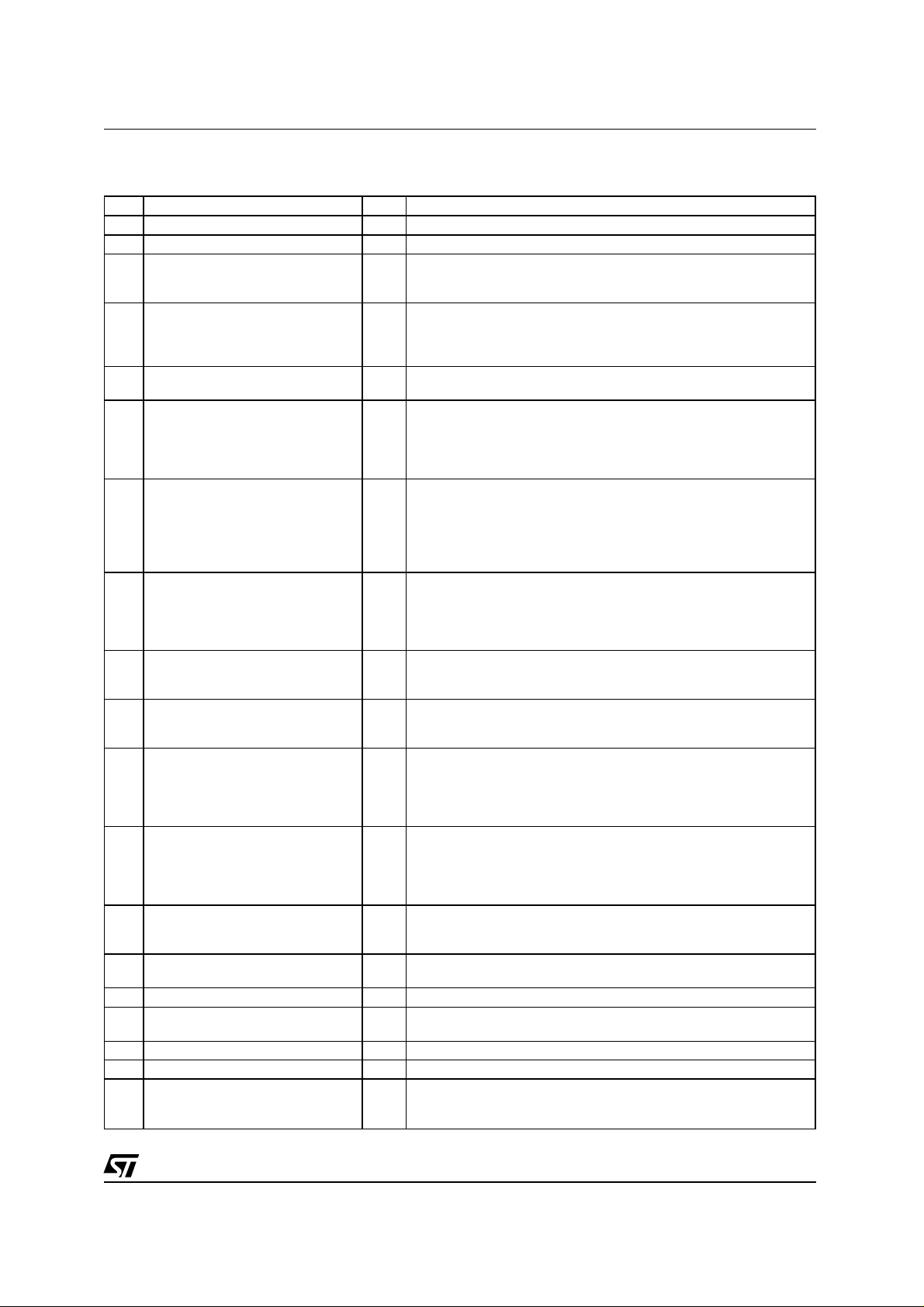
PIN CONNECTION
CODEC0
CODEC2
COUT<5>
COUT<4>
COUT<3>
COUT<2>
COUT<1>
CODEC1
CVDD0
CGND0
COUT<0>
S2DREF
COIN<3>
COIN<2>
COIN<1>
VREF0
VREF1
VREF2
COVDD1
COIN<0>
COGND1
COVDD2
DBRQN0
GND2
VDD2
V
V
2/14
DSP0 GPIO0
DSP0 GPIO1
DSP0 GPIO2
DSP0 GPIO3
DSP0 GPIO4
DSP0 GPIO5
DSP0 GPIO6
DSP0 GPIO7
DSP1 GPIO4
DSP1 GPIO3
DSP1 GPIO2
DSP1 GPIO1
DSP1 GPIO0
TESTEN
TESTSE
NRESET
SCKM
MISOM
MOSIM
SSM
SCKD
MISOD
MOSID
SSD
AVDD
XTI
XTO
CLKIN
AGND
RDSINT
RDSARI_SCLK
RDSQAL_SO
RDSDAT_SI
RDSCLK_SS
INT
SRCCD
SRCMD
GND1
999897
100
1
2
3
4
5
6
7
8
9
10
11
12
13
14
15
16
17
18
19
20
21
22
23
24
25
26
VDD1
9695949392
Test
IIC/SPI master
SPI displa
PLL oscillator
RDS
SPDIF + Sample Rate Converter
272829
3031323334
CGND1
DSRA<7>
DSRA<6>
DSRA<5>
CVDD1
898887
373839
SRA<0>
SRA<1>
8685848382
4041424344
SRA<2>
SRA<3>
SRA<4>
90
91
CODEC
Control Inputs
35
36
DSRA<4>
DSRA<3>
DSRA<2>
DSRA<1>
DSRA<0>
SRA<5>
SRA<6>
SRA<7>
8180797877
Debug DSP0
DSP1
Debu
SAI
EMI
4546474849
SRA<8>
SRA<9>
SRA<10>
SRA<11>
SRA<12>
76
75
74
73
72
71
70
69
68
67
66
65
64
63
62
61
60
59
58
57
56
55
54
53
52
51
50
CGND2
DBCK0OS01
DBIN0OS00
DBOUT0
DBRQN1
DBCK1_OS11
DBIN1_OS10
DBOUT1
LRCKR
SCKR
LRCKT
SCKT
SDI0
SDI1 / SRA<21>
SDI2 / SRA<20>
SDO0 / SRA<19>
SDO1 / SRA<18>
SDO2 / SRA<17>
CASALE
DRD
DWR
SRA<16>
SRA<15>
SRA<14>
SRA<13>
CVDD2
DSP0 GPIO9
DSP0 GPIO11
DSP0 GPIO10
DSP1 GPIO9
DSP1 GPIO11
DSP1 GPIO10
SRCCDC
DSP1 GPIO5
DSP1 GPIO6
DSP1 GPIO7
DSP1 GPIO8
DSP0 GPIO8
Page 3
TDA7500
PIN DESCRIPTION
N° NAME TYPE DESCRIPTION
1 GND1 Ground pin dedicated to the digital periphery.
2 VDD1 Supply pin dedicated to the digital periphery.
3 TESTEN I Test Enable (Input). When active, puts the chip into test mode and
4 TESTSE I SCAN Enable (Input). When active with TESTEN also active,
5 NRESET I System Reset (Input). A low level applied to NRESET input
6 SCKM/DSP0_GPIO0 I/O I
7 MISOM/DSP0_GPIO1 I/O I
8 MOSIM/DSP0_GPIO2 I/O SPI Master Output Slave Input Serial Data (Input/Output)/General
9 SSM/DSP0_GPIO3 I SPI Slave Select (Input)/General Purpose I/O (Input/Output). If SPI
10 SCKD/DSP0_GPIO4 I SPI Bit Clock (Input)/General Purpose I/O (Input/Output). SPI bit
11 MISOD/DSP0_GPIO5 I/O SPI Master Input Slave Output Serial Data (Input/Output)/General
12 MISOD/DSP0_GPIO6 I/O SPI Master Output Slave Input Serial Data (Input/Output)/General
13 SSD/DSP0_GPIO7 I SPI Slave Select (Input)/General Purpose I/O (Input/Output).
14 CLKIN I Clock Input pin (Input). Clock from external digital audio source to
15 AVDD audio source to synchronize the internal PLL.
16 XTI I Crystal Oscillator Input (Input). External Clock Input or crystal
17 XTO O Crystal Oscillator Output (Output). Crystal Oscillator output drive.
18 AGND Ground pin dedicated to the PLL
19 RDSINT/DSP1_GPIO4 O RDS bit/block interrupt (Output)/General Purpose I/O
muxes the XTI clock to all flip-flops. When TEST_SE is also
active, the scan chain shifting is enabled.
controls the shifting of the internal scan chains. When active with
TESTEN not active, sets all tri-state outputs into hi-impedance
mode
initializes the IC.
2
C Serial Clock Line (Input/Output)/SPI Bit Clock (Input)/General
Purpose I/O (Input/Output). Clock line for I
2
C bus. Schmitt trigger
input. If SPI interface is enabled, behaves as SPI bit clock.
Optionally it can be used as general purpose I/O controlled by
DSP0.
2
C Serial Data Line (Input/Output)/SPI Master Input Slave Output
Serial Data (Input/Output)/General Purpose I/O (Input/Output).
Data line for I
2
C bus. Schmitt trigger input. If SPI is enabled,
behaves as Serial Data Input when in SPI Master Mode and Serial
Data Output when in SPI Slave Mode. Optionally it can be used as
general purpose I/O controlled by DSP0.
Purpose I/O (Input/Output). Serial Data Output when in SPI
Master Mode and Serial Data Input when in SPI Slave Mode.
Optionally it can be used as general purpose I/O controlled by
DSP0.
is enabled, behaves as Slave Select line for SPI bus. Optionally it
can be used as general purpose I/O controlled by DSP0.
clock. Schmitt trigger input. Optionally it can be used as general
purpose I/O controlled by DSP0.
Purpose I/O (Input/Output). Schmitt trigger input. Behaves as
Serial Data Input when in SPI Master Mode and Serial Data
Output when in SPI Slave Mode. Optionally it can be used as
general purpose I/O controlled by DSP0.
Purpose I/O (Input/Output). Serial Data Output when in SPI
Master Mode and Serial Data Input when in SPI Slave Mode.
Optionally it can be used as general purpose I/O controlled by
DSP0.
Behaves as Slave Select line for SPI bus. Optionally it can be
used as general purpose I/O controlled by DSP0.
synchronize the internal PLL.
Oscillator input.
(Input/Output). Provides an interrupt to the main micro. Optionally
it can be used as general purpose I/O controlled by DSP1.
3/14
Page 4
TDA7500
PIN DESCRIPTION
N° NAME TYPE DESCRIPTION
20 RDSARI_SCK/DSP1_GPIO3 O SPI Bit Clock (Input)/ARI indicator (Output)/General Purpose I/O
21 RDSQAL_SO/DSP1_GPIO2 O SPI Slave Output Serial Data (Output)/RDS Bit Quality
22 RDSDAT_SI/DSP1_GPIO1 I SPI Slave Input Serial Data (Input)/RDS Bit Data (Output)/General
23 RDSCLK_SS/DSP1_GPIO0 I SPI Chip Select (Input)/RDS Bit Clock (Output)/General Purpose
24 INT I External interrupt line (Input). When this line is asserted low, the
25 CGND1 Ground pin dedicated to the digital core part.
26 CVDD1 Supply pin dedicated to the digital core part.
27 SCRCCD I SPDIF Input 1 (Input). Stereo SPDIF input to connect a digital
28 SCRCMD I SPDIF Input 2 (Input). Stereo SPDIF input to connect a digital
29 DSRA<7> I/O DSP SRAM Data Lines<7> (Input/Output). When in SRAM Mode
30 DSRA<6> I/O DSP SRAM Data Lines<6> (Input/Output). When in SRAM Mode
31 DSRA<5> I/O DSP SRAM Data Lines<5> (Input/Output). When in SRAM Mode
32 DSRA<4> I/O DSP SRAM Data Lines<4> (Input/Output). When in SRAM Mode
33 DSRA<3> I/O DSP SRAM Data Line<3> (Input/Output)/DSP DRAM Data
34 DSRA<2> I/O DSP SRAM Data Line<2> (Input/Output)/DSP DRAM Data
35 DSRA<1> I/O DSP SRAM Data Line<1> (Input/Output)/DSP DRAM Data
36 DSRA<0> I/O DSP SRAM Data Line<0> (Input/Output)/DSP DRAM Data
37 SRA<0> O DSP SRAM Address Line<0> (Output)/DSP DRAM Address
38 SRA<1> O DSP SRAM Address Line<1> (Output)/DSP DRAM Address
(continued)
(Input/Output). Schmitt trigger input. If SPI interface is enabled,
behaves as SPI bit clock. Optionally it provides the ARI indication
bit. Optionally it can be used as general purpose I/O controlled by
DSP1.
(Output)/General Purpose I/O (Input/Output). If SPI is enabled,
behaves as Serial Data Output. Optionally it provides the RDS
serial data quality information. Optionally it can be used as general
purpose I/O controlled by DSP1.
Purpose I/O (Input/Output). If SPI is enabled, behaves as Serial
Data Input. Optionally it provides the RDS serial data stream.
Optionally it can be used as general purpose I/O controlled by
DSP1.
I/O (Input/Output). If SPI is enabled, behaves as Chip Select line
for SPI bus. Optionally it provides the 1187.5Hz RDS Bit Clock.
Optionally it can be used as general purpose I/O controlled by
DSP1.
DSP may be interrupted.
audio source like a CD.
audio source like a MD.
this pin act as the EMI data line 7.
this pin act as the EMI data line 6.
this pin act as the EMI data line 5.
this pin act as the EMI data line 4.
Line<3> (Input/Output). This pin act as the EMI data line 3 in both
SRAM Mode and DRAM Mode.
Line<2> (Input/Output). This pin act as the EMI data line 2 in both
SRAM Mode and DRAM Mode.
Line<1> (Input/Output). This pin act as the EMI data line 1 in both
SRAM Mode and DRAM Mode.
Line<0> (Input/Output). This pin act as the EMI data line 0 in both
SRAM Mode and DRAM Mode.
Line<0> (Output). This pin act as the EMI address line 0 in both
SRAM Mode and DRAM Mode.
Line<1> (Output). This pin act as the EMI address line 1 in both
SRAM Mode and DRAM Mode.
4/14
Page 5
TDA7500
PIN DESCRIPTION
N° NAME TYPE DESCRIPTION
39 SRA<2> O DSP SRAM Address Line<2> (Output)/DSP DRAM Address
40 SRA<3> O DSP SRAM Address Line<3> (Output)/DSP DRAM Address
41 SRA<4> O DSP SRAM Address Line<4> (Output)/DSP DRAM Address
42 SRA<5> O DSP SRAM Address Line<5> (Output)/DSP DRAM Address
43 SRA<6> O DSP SRAM Address Line<6> (Output)/DSP DRAM Address
44 SRA<7> O DSP SRAM Address Line<7> (Output)/DSP DRAM Address
45 SRA<8> O DSP SRAM Address Line<8> (Output)/DSP DRAM Address
46 SRA<9> O DSP SRAM Address Line<9> (Output)/DSP DRAM Address
47 SRA<10> O DSP SRAM Address Line<10> (Output)/DSP DRAM Address
48 SRA<11> O DSP SRAM Address Line<11> (Output)/DSP DRAM Address
49 SRA<12> O DSP SRAM Address Line<12> (Output)/DSP DRAM Address
50 CGND2 Ground pin dedicated to the digital core part.
51 CVDD2 Supply pin dedicated to the digital core part.
52 SRA<13> O DSP SRAM Address Line<13> (Output)/DSP DRAM Address
53 SRA<14> O DSP SRAM Address Line<14> (Output)/DSP DRAM Address
54 SRA<15> O DSP SRAM Address Line<15> (Output)/DSP DRAM Address
55 SRA<16>/DSP0_GPIO8 O DSP SRAM Address Line<16> (Output)/DSP DRAM Address
56 DWR O DSP SRAM Write Enable (Output)/DRAM Write Enable (Output).
57 DRD O DSP SRAM Read Enable(Output)/DRAM Read Enable (Output).
(continued)
Line<2> (Output). This pin act as the EMI address line 2 in both
SRAM Mode and DRAM Mode.
Line<3> (Output). This pin act as the EMI address line 3 in both
SRAM Mode and DRAM Mode.
Line<4> (Output). This pin act as the EMI address line 4 in both
SRAM Mode and DRAM Mode.
Line<5> (Output). This pin act as the EMI address line 5 in both
SRAM Mode and DRAM Mode.
Line<6> (Output). This pin act as the EMI address line 6 in both
SRAM Mode and DRAM Mode.
Line<7> (Output). This pin act as the EMI address line 7 in both
SRAM Mode and DRAM Mode.
Line<8> (Output). This pin act as the EMI address line 8 in both
SRAM Mode and DRAM Mode.
Line<9> (Output). This pin act as the EMI address line 9 in both
SRAM Mode and DRAM Mode.
Line<10> (Output). This pin act as the EMI address line 10 in both
SRAM Mode and DRAM Mode.
Line<11> (Output). This pin act as the EMI address line 11 in both
SRAM Mode and DRAM Mode.
Line<12> (Output). This pin act as the EMI address line 12 in both
SRAM Mode and DRAM Mode.
Line<13> (Output). This pin act as the EMI address line 13in both
SRAM Mode and DRAM Mode.
Line<14> (Output). This pin act as the EMI address line 14 in both
SRAM Mode and DRAM Mode.
Line<15> (Output). This pin act as the EMI address line 15 in both
SRAM Mode and DRAM Mode.
Line<16> (Output)/General Purpose I/O (Input/Output). This pin
acts as the EMI address line 16 in both SRAM Mode and DRAM
Mode. Optionally it can be used as general purpose I/O controlled
by DSP0.
This pin serves as the write enable for the EMI in both DRAM and
SRAM Mode.
This pin serves as the read enable for the EMI in both DRAM and
SRAM Mode.
5/14
Page 6

TDA7500
PIN DESCRIPTION
N° NAME TYPE DESCRIPTION
58 CASALE O DSP DRAM Column Address Strobe (Output). When in DRAM
59 SDO<2>/SRA<17>/DSP1_GPIO<8>O SAI Outputs (Output)/EMI SRAM Address Line<17>
60 SDO<2>/SRA<18>/DSP1_GPIO<7>O SAI Outputs (Output)/EMI SRAM Address Line<18>
61 SDO<0>/SRA<19> O SAI Output (Output)/EMI SRAM Address Line<19> (Output). One
62 SDI<2>/SRA<20>/DSP1_GPIO<6> I SAI Input (Input)/EMI SRAM Address Line<20> (Output)/General
63 SDI<1>/SRA<21>/RAS/DSP1_GPIO<5> I SAI Input (Input)/EMI SRAM Address Line<21> (Output)/DRAM
64 SDI<0>/SRCCDC I SAI Input (Input)/SPDIF Input 3 (Input). One stereo channel SAI
65 SCKT I/O SAI transmitter Bit Clock (Input/Output). SAI transmitter bit clock.
66 LRCKT I/O SAI transmitter Left-Right Clock (Input/Output). SAI transmitter
67 SCKR I/O SAI receiver Bit Clock (Input/Output). SAI receiver bit clock.
68 LRCKR I/O SAI receiver Left-Right Clock (Input/Output). SAI receiver Left-
69 DBOUT1/DSP1_GPIO10 I/O Debug Port Serial Output (Input/Output)/ General Purpose I/O
70 DBIN1/OS10/DSP1_GPIO11 I/O Debug Port Serial Input/Chip Status 0 (Input/Output)/ General
71 DBCK1/OS11/DSP1_GPIO9 I/O Debug Port Bit Clock/Chip Status 1 (Input/Output)/General
72 DBRQN1 I Debug Port Request Input (Input). Means of entering the Debug
73 DBOUT0/DSP0_GPIO10 I/O Debug Port Serial Output (Input/Output)/ General Purpose I/O
74 DBIN0/OS00/DSP0_GPIO11 I/O Debug Port Serial Input/Chip Status 0 (Input/Output)/ General
(continued)
Mode this pin acts as the column address strobe.
(Output)/General Purpose I/O (Input/Output). One stereo channel
SAI data output in SAI mode. EMI address line 17 in SRAM Mode.
Optionally it can be used as a general purpose I/O.
(Output)/General Purpose I/O (Input/Output). One stereo channel
SAI data output in SAI mode. EMI address line 18 in SRAM Mode.
Optionally it can be used as a general purpose I/O.
stereo channel SAI data output in SAI mode. EMI address line 19
in SRAM Mode.
Purpose I/O (Input/Output). One stereo channel SAI data input in
SAI mode. EMI address line 20 in SRAM Mode. Optionally it can
be used as a general purpose I/O.
Row Address Strobe (Output)/General Purpose I/O (Input/Output).
One stereo channel SAI data input in SAI mode. EMI address line
21 in SRAM Mode. When in DRAM Mode this pin acts as the row
address strobe. Optionally it can be used as a general purpose I/O.
data input in SAI mode. Stereo SPDIF input intended to connect a
digital audio source like a CD changer in SPDIF mode.
Master or slave.
Left-Right clock. Can be master or slave mode.
Right clock.
(Input/Output). The serial data output for the Debug Port.
Optionally it can be used as a general purpose I/O.
Purpose I/O (Input/Output). The serial data input for the Debug
Port is provided when an input. When an output, together with
OS1 provides information about the chip status. Optionally it can
be used as a general purpose I/O.
Purpose I/O (Input/Output). The serial clock for the Debug Port is
provided when an input. When an output, together with OS0
provides information about the chip status. Optionally it can be
used as a general purpose I/O.
mode of operation.
(Input/Output). The serial data output for the Debug Port.
Optionally it can be used as a general purpose I/O.
Purpose I/O (Input/Output). The serial data input for the Debug
Port is provided when an input. When an output, together with
OS1 provides information about the chip status. Optionally it can
be used as a general purpose I/O.
6/14
Page 7

TDA7500
PIN DESCRIPTION
N° NAME TYPE DESCRIPTION
75 DBCK0/OS01/DSP0_GPIO9 I/O Debug Port Bit Clock/Chip Status 1 (Input/Output)/General
76 DBRQN0 I Debug Port Request Input (Input). Means of entering the Debug
77 VDD2 Supply pin dedicated to the digital periphery.
78 GND2 Ground pin dedicated to the digital periphery.
79 ADC<0> I Analog Inputs (Input). Single ended analog signal inputs to the
80 ADC<1> I Analog Inputs (Input). Single ended analog signal inputs to the
81 ADC<2> I Analog Inputs (Input). Single ended analog signal inputs to the
82 ADC<3> I Analog Inputs (Input). Single ended analog signal inputs to the
83 S2DREF I Voltage Reference (Input). External decoupling of the analog
84 ADCVDDREF I Voltage Reference (Input). Analog voltage reference input. Signal
85 ADCREF<2> I Voltage Reference (Input). External decoupling of the analog
86 ADCREF<1> I Voltage Reference (Input). External decoupling of the analog
87 ADCREF<0> I Voltage Reference (Input). External decoupling of the analog
88 ADCVDD Analog Supply pin dedicated to the A/D converter.
89 ADCGND Analog Ground pin dedicated to the A/D converter.
90 DAC<0> O Analog Outputs (Output). Analog signal outputs of the DAC
91 DAC<1> O Analog Outputs (Output). Analog signal outputs of the DAC
92 DAC<2> O Analog Outputs (Output). Analog signal outputs of the DAC
93 DAC<3> O Analog Outputs (Output). Analog signal outputs of the DAC
94 DAC<4> O Analog Outputs (Output). Analog signal outputs of the DAC
95 DAC<5> O Analog Outputs (Output). Analog signal outputs of the DAC
96 DACREF<2> I Voltage Reference (Input). External decoupling of the analog
97 DACREF<1> I Voltage Reference (Input). External decoupling of the analog
98 DACREF<0> I Voltage Reference (Input). External decoupling of the analog
99 DACGND Analog Ground pin dedicated to the D/A converter.
100 DACVDD Analog Supply pin dedicated to the D/A converter.
(continued)
Purpose I/O (Input/Output). The serial clock for the Debug Port is
provided when an input. When an output, together with OS0
provides information about the chip status. Optionally it can be
used as a general purpose I/O.
mode of operation.
ADC.
ADC.
ADC.
ADC.
reference used for the single to differential ended converter.
is supplied by A354.
references used for the sigma delta modulator.
references used for the sigma delta modulator.
references used for the sigma delta modulator.
references of the CODEC.
references of the CODEC.
references of the CODEC.
7/14
Page 8

TDA7500
RECOMMENDED DC OPERATING CONDI TIONS
Symbol Parameter Test Condition Min. Typ. Max. Unit
V
DDC
T
j
POWER CONSUMPTION
Symbol Parameter Value Unit
I
dd
Note: 43MHz internal DSP clock at Tamb
3.3V Power Supply Voltage 3 3.3 3.6 V
Operating Junction Temperature -40 125 °C
Maximum current for core power supply @3.3V 450 mA
ADC PERFORMANCE
(T = 25°C, AV
Symbol Parameter Test Condition Min. Typ. Max. Unit
(1) Corresponding to 2VRMS Maximum Differential Input.
DD
Maximum input level (1) 1 Vrms
Sample rate 32 48 KHz
Frequency Response @ 20KHz with f
Instant Dynamic Range -60dB analog input 90 93 dB
SNR 1KHz; -3dB analog input 90 93 dB
(THD + N)/S -3dB analog input -85 dB
PSRR 0.1Vp @ 1KHz 45 dB
Input Impedance 10 30 K
Crosstalk 1Vrms input @ 15KHz 70 dB
Gain mismatch between four
input
CMRR @ 1KHz 40 dB
CM Input range 100 mV
DAC PERFORMANCE
(T = 25°C, AV
DD
Some of the relevant ADC parameters are reported in the following table:
= 3.3V, measurement bandwidth 10Hz to 20KHz, A-Weighted Filter.)
= 44.1KHz -3 dB
s
@ 1KHz -0.5 0.5 dB
Some of the relevant DAC parameters are reported in the following table:
= 3.3V, measurement bandwidth 10Hz to 20KHz, A-Weighted Filter 0dB gain, output
load 30kΩ)
Symbol Parameter Test Condition Min. Typ. Max. Unit
Maximum output level (1) 1 Vrms
Sample rate 32 48 KHz
Frequency Response @ 20KHz with f
Dynamic Range -60dB analog input 90 93 dB
SNR 1KHz -3dB analog output 90 93 dB
Total D R 100 dB
Digital Silence 0000$ digital input 93 dB
(THD + N)/S -3dB analog input -85 dB
PSRR 0.1Vp @ 1KHz 45 dB
Output Impedance 30 k
Crosstalk 1Vrms output @ 15KHz 70 dB
Gain mismatch between six
outputs
(1) Corresponding to 2VRMS Maximum Differential Output.
@ 1KHz -0.5 0.5 dB
= 44.1KHz -3 dB
s
Ω
Ω
8/14
Page 9

FUNCTIONAL DESCRIPTION.
The TDA7500 IC broken up into two distinct
blocks. One block contains the two DSP Cores
and their associated peripherals. The other contains the ADC, DAC and the RDS filter, demodulator and decoder.
24-BIT DSP CORE.
The two DSP cores are used to process the
audio and FM/AM data, coming from the ADC,
either any kind of digital data coming via SPDIF
or SAI. After the digital signal processing these
data are sent to the DAC for analog c onversion.
Functions such as volume, tone, balance, and
fader control, as well as spatial enhancement and
general purpose signal processing may be performed by the DSP0. When FM/AM mode is selected, DSP1 is fully devoted to AM/FM processing. Nevertheless it can be used for any kind of
different application, when a different input
source is selected.
Some capabilities of the DSPs are listed below:
Single cycl e multiply and a ccumulate with c onvergent rounding and condition code generation
2 x 56-bit Accumulators
Double precision multiply
Scaling and saturation arithmetic
48-bit or 2 x 24-bit parallel moves
64 interrupt vector locations
Fast or long interrupts possible
Programmable interrupt priorities and masking
8 each of Address Registers, Address Offset
Registers and Address Modulo Registers
Linear, Reverse Carry, Multiple Buffer Modulo,
Multiple Wrap-around Modulo address arithmetic
Post-increment or decrement by 1 or by offset,
Index by offset, predecrement address
Repeat instruction and zero overhead DO
loops
Hardware stack capable of nesting combinations of 7 DO loops or 15 interrupts/subroutines
Bit manipulation instructions possible on all
registers and memory locations. Also Jump on
bit test.
4 pin serial debug interface
Debug ccess to all internal registers, buses
and memory locations
5 word deep program address history FIFO
Hardware and software breakpoints for both
program and data memory accesses
Debug Single stepping, Instruction injection
and Disassembly of program memory
TDA7500
DSP PERI PH E R A L S
There are a number of peripherals that are tightly
coupled to the two DSP Cores. Same of the peripherals are connected to DSP 0 others are connected to DSP1.
512 x 24-Bit X-RAM.
512 x 24-Bit Y-RAM.
1024 x 24-Bit Program RAM (5.5K x 24 for
DSP1)
128 x 24-Bit Boot ROM for each DSP.
Serial Audio Interface (SAI)
SPDIF receiver with sampling rate conversion
I2C and SPI interface
XCHG Interface for DSP to DSP communica-
tion.
External Memory Interface (DRAM/SRAM) for
time-delay and traffic information.
Double Debug Port
DATA AND PROGRAM MEMORY
Both DSP0 and DSP1 have an identical set of
Data and Program memories attached to them.
Each of the memories are described below and it
is implied that there ar e two of each type, one set
connected to DSP0 and the ot her to DSP1. The
only exception is the case of the P-RAM where
DSP0 has a 1024 x 24-Bit P RAM and DSP1 has
a 5.5K x 24-Bit PRAM.
512 x 24-Bit X-RAM (XRAM)
This is a 512 x 24-Bit Single Port SRAM used for
storing coefficients. The 16-Bit XRAM address,
XABx(15:0) is generated by the Address Generation Unit of the DSP core. The 24-Bit XRAM Data,
XDBx(23:0), may be written to and read from the
Data ALU of the DSP core. The XDBx Bus is also
connected to the Internal Bus Switch so that it
can be routed to and from all peripheral blocks.
512 x 24 Bit Y-RAM (YRAM)
This is a 512 x 24-Bit Single Port SRAM used for
storing coefficients. The 16-Bit address,
YABx(15:0) is generated by the Address Generation Unit of the DSP core. The 24-Bit Data,
YDBx(23:0), is written to and read from the Data
ALU of the DSP core. The YDBx Bus is also connected to the Internal Bus Switch so that it can be
routed to and from other blocks.
1024 x 24-Bit Program RAM (PRAM 5.5K x 24-bit
for DSP1)
This is a 1024 x 24-Bit Single Port SRAM used
for storing and executing program code. The 16-
9/14
Page 10

TDA7500
Bit PRAM Address, PABx(15:0) is generated by
the Program Address Generator of the DSP core
for Instruction Fetching, and by the AGU in the
case of the Move Program Memory (MOVEM) Instruction. The 24-Bit PRAM Data (Program
Code), PDBx(23:0), can only be written to using
the MOVEM instruction. During instruction fetching the PDBx Bus is routed to the Program Decode Controller of the DSP core for instruction
decoding.
256 x 24-Bit Bootstrap ROM (PROM)
This is a 256 x 24- Bi t fa ctor y pr ogr amm ed Boot RO M
used for storing the pro gra m s eque nc e and f or init ializing the DSP. Essent ia lly thi s cons is ts of reading the
data via I
2
C, SPI or EMI interface and store it in
PRAM, XRAM , YRAM, and/or exter nal DRA M.
Serial Audio Interface (SAI)
The SAI is used to deliver digital audio to the
DSPs from an external source. Once processed
by the DSPs, it can be returned through this interface either sent to the DAC for D/A conversion.
The features of the SAI are listed below.
3 Synchronized Stereo Data Transmission
Lines
3 Synchronized Stereo Data Reception Lines
Master and Slave operating mode: clock lines
can be both master and slave.
Receive and Transmit Data Registers have
two locations to hold left and right data.
XCHG Interface (DSP to DSP Exchange Interface)
The Exchange Interface peripheral provides bidirectional communication between DSP0 and
DSP1. Both 24 bit word data and four bit Flag
data can be exchanged. A FIFO is utilized for received data. It minim izes the number of t imes an
Exchange Interrupt Service Routine would have
to be called if multi-word blocks of data were to
be received. The Transmit FIFO is in effect the
Receive FIFO of the other DSP and is written directly by the transmitting DSP. The features of
the XCHG are listed below.
10 Word XCHG Receive FIFO on both DSPs
Four Flags for each XCHG for DSP to DSP
signaling
Condition flags can optionally trigger interrupts
on both DSPs
DRAM/SRAM Interface (EMI)
The External DRAM/SRAM Interface is viewed as
a memory mapped peripheral. Data transfers are
performed by moving data into/from data registers and the control is exercised by polling status
flags in the control/status r egister or by servicing
interrupts. An external memory write is executed
by writing data into the EMI Data Write Register.
An external memory read operation is executed
by either writing to the offset register or reading
the EMI Data Read Register, depending on the
configuration.
The features of the EMI are listed below.
Data bus width fixed at 4 bits for DRAM and 8
bits for SRAM.
Data word length 16 or 24 bits for DRAM.
Data word length 8or 16 or 24 bits for SRAM.
Thirteen DRAM address lines means 226 =
32MB addressable DRAM.
Refresh rate for DRAM can be chosen among
eight divider factor.
SRAM relative addressing mode; 222 = 4MB
addressable SRAM.
Four SRAM Timing choices.
Two Read Offset Registers.
Debug Interface
A dedicated Debug Port is available for each DSP
Cores. The debug logic is contained in the core
design of the DSP. The features of the Debug
Port are listed below:
Breakpoint Logic
Trace Logic
Single stepping
Instruction Injection
Program Disassembly
Serial Peripheral Interface
The DSP core requires a serial interface to receive commands and data over the LAN. During
an SPI transfer, data is transmitted and received
simultaneously. A serial clock line synchronizes
shifting and sampling of the information on the
two serial data lines. A slave select line allows individual selection of a slave SPI device.
When an SPI transfer occurs an 8-bit word is
shifted out one data pin while another 8-bit character is simultaneously shifted in a second data
pin.
The central element in the SPI system is the shift
register and the read data buffer. The system is
single buffered in the trans fer direction and double buffered in the receive direction.
2
C Interface
I
The inter Integrated Circuit bus is a single bidirectional two-wire bus used for efficient inter IC control. All I
an on-chip interface which allows them communicate directly with each other via the I
2
C bus compatible devices incorporate
2
C bus.
10/14
Page 11

TDA7500
Every component hooked up to the I2C bus has
its own unique address whether it is a CPU,
memory or some other complex function chip.
Each of these chips can act as a receiver and /or
transmitter on its functionality.
General Purpose Input/Output
The DSP requires a set of external general purpose input/output lines, and a reset line. These
signals are used by external devices to signal
events to the DSP. The GPIO lines are implemented as DSP ’s peripherals. The GPIO lines
are grouped in Port A which is connected to DSP
0, and Port B, which is connected to DSP1.
PLL Clock Oscillator
The PLL Clock Oscillator can accept an external
clock at XTI or it can be configured to run an internal oscillator when a crystal is connected
across pins XTI & XTO. There is an input divide
block IDF (1 -> 32) at the XTI clock input and a
multiply block MF (9 -> 128) in the PLL loop.
Hence the PLL can multiply the external input
clock by a ratio MF/IDF to generate the internal
clock. This allows the internal clock to be within 1
MHz of any desired frequency even when XTI is
much greater than 1 MHz. It is recommended that
the input clock is not divided down to le ss than 1
MHz as this reduces the Phase Detector’s update
rate.
The clocks to the DSP can be selected to be
either the VCO output divided by 2 to 16, or be
driven by the XTI pin directly.
The crystal oscillator and the PLL will be gated off
when entering the power-down mode (by setting
a register on DSP0).
93dB D/A Dynamic Range (A-Weighted)
93dB A/D Dynamic Range (A-Weighted)
85dB D/A (THD+N/S)
85dB A/D (THD+N/S)
Internal Differential Analog Architecture
+3.3V Power Supply
SOFTWARE FEATURES
A great flexibility is guaranteed by the two programmable DSP cores. A list of th e main software functions wh ich can be imple men te d in the TDA750 0 is
enclosed hereafter. A block diagram of the audio
proce s s ing fl ow is sh ow n in Fi g . 1 below.
AM/FM Baseband Signal Processing
FM weak signal processing
Integrated 19 kHz MPX filter and deemphasis
flexible noise cancellation
flexible multipath detector
Generic Audio Signal Processsing
Loudness
Bass, treble, fader control
Volume control
Distortion Limiting
Premium Equalization
Soft mute
TAPE Signal Processsing
Dolby B Noise Reduction
Automatic Mu sic Search
CD Signal Proceessing
Dynamic Range Compression
Codec
The CODEC is composed of four AD mono converters, three DA stereo converters. The ADC
can operate both in audio mode and in FM/AM
mode. When in audio mode, it converts the audio
bandwidth from 20 to 20KHz. The A to D is a third
order Sigma-Delta converter, the converter resolutions is 20 bit with 93 dB of dynamic range and
85dB of total harmonic distortion. When in FM
mode, the converted bandwidth is up t o 192KHz.
The D to A is a third order Sigma-Delta converter
with a low noise reconstructing analog filter, the
converter resolution is 20 bit with 93 dB of dynamic range and 85dB of total harmonic distortion. All the reference voltages are generated inside the chip.
Some capabilities of the CODEC are listed below:
20-Bit Resolution
Digital Anti-Alias Filtering embedded
Adjustable System Sampling Rates
Audiophile (optional)
Parametric Equalization
Crossover Patters
Channel Delays
Center Channel Imaging Output
Audio Noise Reduction
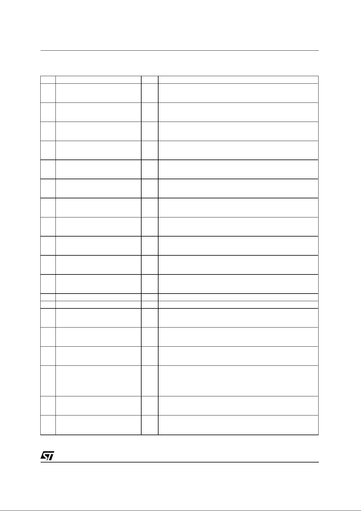
Application Scheme
The TDA7500 can operate as a standalone device either it can interface the TDA7501 which
contains the analog input multiplexer, analog volume control and the line-driver. The FM_MPX
and FM_LEVEL signals coming from the tuner
and other signals supplied by analog sour ces are
adapted by the TDA7501 and fed to the
TDA7500. A block diagram of the system is
shown in Fig.2 below.
The TDA7500 converts all the analog signals into
11/14
Page 12

y
g
g
TDA7500
digital domain and performs AM/FM processing
and audio/sound processing. Thanks to this, it is
possible to process any audio source as well analog as digital in parallel, to record FM mono for
tion and RDS. Finally the digital signals are D/A
converted and sent to the TDA7501 for the final
level adjustment and for the analog volume control.
traffic information, telephone response, naviga-
Figure 1. Software Block Diagram of Audio & Sound Processing
ANR SM
Stereo
input
Audio
noise
reduction
D
namic
e
Loudness
ran
compression
Bass Treble Parametric
equaliser
Soft
mute
Figure 2. Block Diagram of Car Amplifier Audio Sub-System.
DLY
HPPEQTBLDDRC
+
HPPEQTBLDDRCANR SM
RM
DLY
DLY
DLY
DLY
Delay
LP
Routin
matrix
RF
CF
LF
RR
LR
SW
FRONT END
TDA7421
MAIN
MICRO
2
I
C/SPI
EEPROM/
FLASH
ANALOG INPUT
TDA7501
A/D D/A
TDA7500
SPDIF
DIGITAL IN
DRAM/
SRAM
AUDIO POWER
DISPLAY
MICRO
DIGITAL OUT
D98AU946A
12/14
Page 13

TDA750 0
DIM.
MIN. TYP. MAX. MIN. TYP. MAX.
mm inch
A 1.60 0.063
A1 0.05 0.15 0.002 0.006
A2 1.35 1.40 1.45 0.053 0.055 0.057
B 0.17 0.22 0.27 0.007 0.009 0.011
C 0.09 0.20 0.003 0.008
D 16.00 0.630
D1 14.00 0.551
D3 12.00 0.472
e 0.50 0.020
E 16.00 0.630
E1 14.00 0.551
E3 12.00 0.472
H 9.85 0.388
L 0.45 0.60 0.75 0.018 0.024 0.030
L1 1.00 0.039
S 8.80 0.346
S1 8.80 0.346
K 0˚ (min.), 3.5˚ (typ.), 7˚(max.)
ccc 0.080 0.003
OUTLIN E AND
MECHANI CAL DATA
TQFP100 (14x14x1.40mm)
with Slug Down (10x10mm)
D
D1
D3
76
e
S1
B
PIN 1
IDENTIFICATION
100
1
H
S
5175
50
E3 E1 E
0.25mm
.010 inch
GAGE PLANE
26
25
TQFP100M
K
L
SEATING
C
PLANE
ccc
C
L1
A
A2
A1
C
13/14
Page 14

TDA7500
Information furnished is believ ed to be accurate and reliable. How ever, STMicroelectr onics assumes no res ponsibility for the co nsequences
of use of such informati on nor for any infringement of patents or other ri ghts of third parties which may result from its use. No license is
granted by im plica tion or otherw ise under any patent or pa tent right s of STMicr oelectronic s. Speci fication mentioned in this publication are
subject to c hange without notice. T hi s publication supersedes and replac es all information prev i ously supplied. STMic roel ectronics produc ts
are not authorized for use as critical components in life support devices or systems without express written approval of STMicroelectronics.
The ST logo is a registered trademark of STMicroelectronics
© 1999 STMicroelectronics – Printed in Italy – All Rights Reserved
STMicroelectronics GROUP OF COMPANIES
Australia - Brazil - China - Finland - France - Germany - Hong Kong - India - Italy - Japan - Malaysia - Malta - Morocco -
Singapore - Spain - Sweden - Switzerland - United Kingdom - U.S.A.
http://www.st.com
14/14
 Loading...