

Page 1

100-watt + 100-watt dual BTL class-D audio amplifier
Features
■ 100-W + 100-W output power at
THD = 10% with R
■ 80-W + 80-W output power at
THD = 10% with R
■ Wide-range single-supply operation (14 - 39 V)
■ High efficiency (η = 90%)
■ Four selectable, fixed gain settings of
nominally 25.6 dB, 31.6 dB, 35.1 dB and
37.6 dB
■ Differential inputs minimize common-mode
noise
■ Standby and mute features
■ Short-circuit protection
■ Thermal overload protection
■ Externally synchronizable
= 6 Ω and V
L
= 8 Ω and V
L
CC
CC
= 36 V
= 34 V
TDA7498
PowerSSO36
with exposed pad up
Description
The TDA7498 is a dual BTL class-D audio
amplifier with single power supply designed for
home systems and active speaker applications.
It comes in a 36-pin PowerSSO package with
exposed pad up (EPU) to facilitate mounting a
separate heatsink.
Table 1. Device summary
Order code Operating temp. range Package Packaging
TDA7498 -40 to 85 °C PowerSSO36 (EPU) Tube
TDA7498TR -40 to 85 °C PowerSSO36 (EPU) Tape and reel
September 2011 Doc ID 16107 Rev 8 1/28
www.st.com
28
Page 2

Contents TDA7498
Contents
1 Pin description . . . . . . . . . . . . . . . . . . . . . . . . . . . . . . . . . . . . . . . . . . . . . 6
1.1 Pinout . . . . . . . . . . . . . . . . . . . . . . . . . . . . . . . . . . . . . . . . . . . . . . . . . . . . . 6
1.2 Pin list . . . . . . . . . . . . . . . . . . . . . . . . . . . . . . . . . . . . . . . . . . . . . . . . . . . . . 7
2 Electrical specifications . . . . . . . . . . . . . . . . . . . . . . . . . . . . . . . . . . . . . . 8
2.1 Absolute maximum ratings . . . . . . . . . . . . . . . . . . . . . . . . . . . . . . . . . . . . . 8
2.2 Thermal data . . . . . . . . . . . . . . . . . . . . . . . . . . . . . . . . . . . . . . . . . . . . . . . 8
2.3 Recommended operating conditions . . . . . . . . . . . . . . . . . . . . . . . . . . . . . 8
2.4 Electrical specifications . . . . . . . . . . . . . . . . . . . . . . . . . . . . . . . . . . . . . . . 8
3 Characterizations . . . . . . . . . . . . . . . . . . . . . . . . . . . . . . . . . . . . . . . . . . 11
3.1 Test circuit . . . . . . . . . . . . . . . . . . . . . . . . . . . . . . . . . . . . . . . . . . . . . . . . 11
3.2 Characterization curves . . . . . . . . . . . . . . . . . . . . . . . . . . . . . . . . . . . . . . 13
3.2.1 For RL = 6 Ω . . . . . . . . . . . . . . . . . . . . . . . . . . . . . . . . . . . . . . . . . . . . . . . . . . .13
3.2.2 For R
= 8 Ω . . . . . . . . . . . . . . . . . . . . . . . . . . . . . . . . . . . . . . . . . . . . . . . . . . .16
L
4 Applications information . . . . . . . . . . . . . . . . . . . . . . . . . . . . . . . . . . . . 19
4.1 Applications circuit . . . . . . . . . . . . . . . . . . . . . . . . . . . . . . . . . . . . . . . . . . 19
4.2 Mode selection . . . . . . . . . . . . . . . . . . . . . . . . . . . . . . . . . . . . . . . . . . . . . 20
4.3 Gain setting . . . . . . . . . . . . . . . . . . . . . . . . . . . . . . . . . . . . . . . . . . . . . . . 21
4.4 Input resistance and capacitance . . . . . . . . . . . . . . . . . . . . . . . . . . . . . . . 21
4.5 Internal and external clocks . . . . . . . . . . . . . . . . . . . . . . . . . . . . . . . . . . . 22
4.5.1 Master mode (internal clock) . . . . . . . . . . . . . . . . . . . . . . . . . . . . . . . . . 22
4.5.2 Slave mode (external clock) . . . . . . . . . . . . . . . . . . . . . . . . . . . . . . . . . . 22
4.6 Output low-pass filter . . . . . . . . . . . . . . . . . . . . . . . . . . . . . . . . . . . . . . . . 23
4.7 Protection functions . . . . . . . . . . . . . . . . . . . . . . . . . . . . . . . . . . . . . . . . . 24
4.8 Diagnostic output . . . . . . . . . . . . . . . . . . . . . . . . . . . . . . . . . . . . . . . . . . . 24
5 Package mechanical data . . . . . . . . . . . . . . . . . . . . . . . . . . . . . . . . . . . . 25
6 Revision history . . . . . . . . . . . . . . . . . . . . . . . . . . . . . . . . . . . . . . . . . . . 27
2/28 Doc ID 16107 Rev 8
Page 3

TDA7498 List of figures
List of figures
Figure 1. Internal block diagram (showing one channel only) . . . . . . . . . . . . . . . . . . . . . . . . . . . . . . . 5
Figure 2. Pin connections (top view, PCB view) . . . . . . . . . . . . . . . . . . . . . . . . . . . . . . . . . . . . . . . . . 6
Figure 3. Test circuit for characterizations . . . . . . . . . . . . . . . . . . . . . . . . . . . . . . . . . . . . . . . . . . . . 11
Figure 4. Test board . . . . . . . . . . . . . . . . . . . . . . . . . . . . . . . . . . . . . . . . . . . . . . . . . . . . . . . . . . . . . 12
Figure 5. Output power (THD = 10%) vs. supply voltage . . . . . . . . . . . . . . . . . . . . . . . . . . . . . . . . . 13
Figure 6. THD vs. output power . . . . . . . . . . . . . . . . . . . . . . . . . . . . . . . . . . . . . . . . . . . . . . . . . . . . 13
Figure 7. THD vs. frequency (1 W) . . . . . . . . . . . . . . . . . . . . . . . . . . . . . . . . . . . . . . . . . . . . . . . . . . 14
Figure 8. THD vs. frequency (100 mW) . . . . . . . . . . . . . . . . . . . . . . . . . . . . . . . . . . . . . . . . . . . . . . 14
Figure 9. Frequency response . . . . . . . . . . . . . . . . . . . . . . . . . . . . . . . . . . . . . . . . . . . . . . . . . . . . . 14
Figure 10. FFT performance (0 dBFS) . . . . . . . . . . . . . . . . . . . . . . . . . . . . . . . . . . . . . . . . . . . . . . . . 15
Figure 11. FFT performance (-60 dBFS) . . . . . . . . . . . . . . . . . . . . . . . . . . . . . . . . . . . . . . . . . . . . . . 15
Figure 12. Output power (THD = 10%) vs. supply voltage . . . . . . . . . . . . . . . . . . . . . . . . . . . . . . . . . 16
Figure 13. THD vs. output power . . . . . . . . . . . . . . . . . . . . . . . . . . . . . . . . . . . . . . . . . . . . . . . . . . . . 16
Figure 14. THD vs. frequency (1 W) . . . . . . . . . . . . . . . . . . . . . . . . . . . . . . . . . . . . . . . . . . . . . . . . . . 17
Figure 15. THD vs. frequency (100 mW) . . . . . . . . . . . . . . . . . . . . . . . . . . . . . . . . . . . . . . . . . . . . . . 17
Figure 16. Frequency response . . . . . . . . . . . . . . . . . . . . . . . . . . . . . . . . . . . . . . . . . . . . . . . . . . . . . 17
Figure 17. FFT performance (0 dB) . . . . . . . . . . . . . . . . . . . . . . . . . . . . . . . . . . . . . . . . . . . . . . . . . . 18
Figure 18. FFT performance (-60 dB) . . . . . . . . . . . . . . . . . . . . . . . . . . . . . . . . . . . . . . . . . . . . . . . . . 18
Figure 19. Applications circuit for 6- or 8-Ω speakers . . . . . . . . . . . . . . . . . . . . . . . . . . . . . . . . . . . . . 19
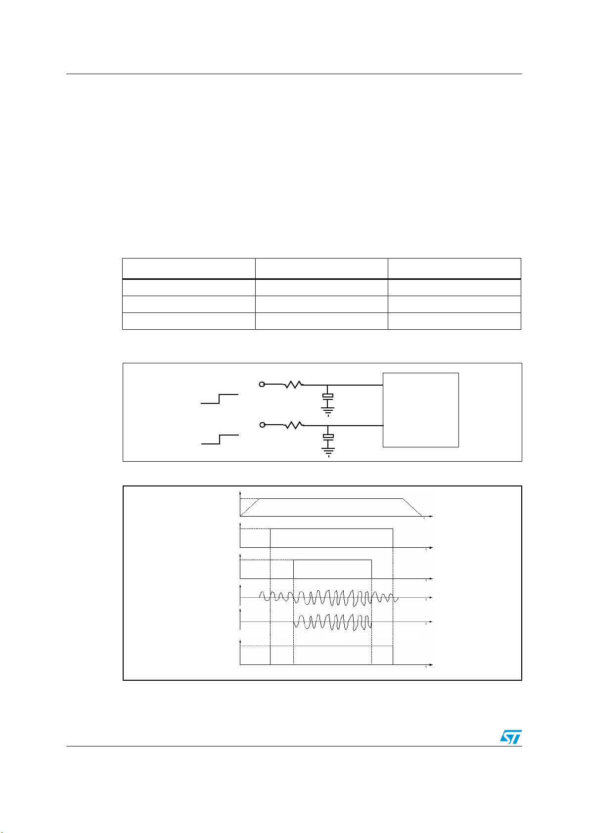
Figure 20. Standby and mute circuits . . . . . . . . . . . . . . . . . . . . . . . . . . . . . . . . . . . . . . . . . . . . . . . . . 20
Figure 21. Turn on/off sequence for minimizing speaker “pop” . . . . . . . . . . . . . . . . . . . . . . . . . . . . . 20
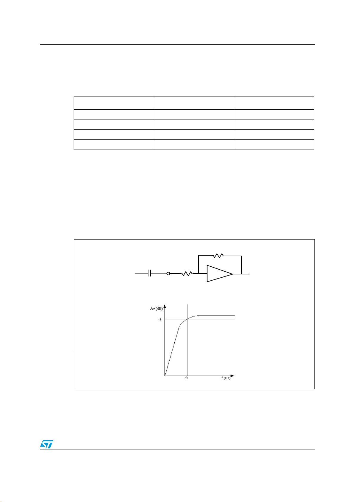
Figure 22. Input circuit and frequency response . . . . . . . . . . . . . . . . . . . . . . . . . . . . . . . . . . . . . . . . . 21
Figure 23. Master and slave connection . . . . . . . . . . . . . . . . . . . . . . . . . . . . . . . . . . . . . . . . . . . . . . . 22
Figure 24. Typical LC filter for a 8-Ω speaker . . . . . . . . . . . . . . . . . . . . . . . . . . . . . . . . . . . . . . . . . . . 23
Figure 25. Typical LC filter for a 6-Ω speaker . . . . . . . . . . . . . . . . . . . . . . . . . . . . . . . . . . . . . . . . . . . 23
Figure 26. Behavior of pin DIAG for various protection conditions . . . . . . . . . . . . . . . . . . . . . . . . . . . 24
Figure 27. PowerSSO36 EPU outline drawing . . . . . . . . . . . . . . . . . . . . . . . . . . . . . . . . . . . . . . . . . . 26
Doc ID 16107 Rev 8 3/28
Page 4

List of tables TDA7498
List of tables
Table 1. Device summary . . . . . . . . . . . . . . . . . . . . . . . . . . . . . . . . . . . . . . . . . . . . . . . . . . . . . . . . . . 1
Table 2. Pin description list . . . . . . . . . . . . . . . . . . . . . . . . . . . . . . . . . . . . . . . . . . . . . . . . . . . . . . . . . 7
Table 3. Absolute maximum ratings . . . . . . . . . . . . . . . . . . . . . . . . . . . . . . . . . . . . . . . . . . . . . . . . . . 8
Table 4. Thermal data. . . . . . . . . . . . . . . . . . . . . . . . . . . . . . . . . . . . . . . . . . . . . . . . . . . . . . . . . . . . . 8
Table 5. Recommended operating conditions . . . . . . . . . . . . . . . . . . . . . . . . . . . . . . . . . . . . . . . . . . 8
Table 6. Electrical specifications. . . . . . . . . . . . . . . . . . . . . . . . . . . . . . . . . . . . . . . . . . . . . . . . . . . . . 8
Table 7. Mode settings . . . . . . . . . . . . . . . . . . . . . . . . . . . . . . . . . . . . . . . . . . . . . . . . . . . . . . . . . . . 20
Table 8. Gain settings . . . . . . . . . . . . . . . . . . . . . . . . . . . . . . . . . . . . . . . . . . . . . . . . . . . . . . . . . . . . 21
Table 9. How to set up SYNCLK . . . . . . . . . . . . . . . . . . . . . . . . . . . . . . . . . . . . . . . . . . . . . . . . . . . 22
Table 10. PowerSSO36 EPU dimensions . . . . . . . . . . . . . . . . . . . . . . . . . . . . . . . . . . . . . . . . . . . . . 25
Table 11. Document revision history . . . . . . . . . . . . . . . . . . . . . . . . . . . . . . . . . . . . . . . . . . . . . . . . . 27
4/28 Doc ID 16107 Rev 8
Page 5

TDA7498 Device block diagram
Device block diagram
Figure 1 shows the block diagram of one of the two identical channels of the TDA7498.
Figure 1. Internal block diagram (showing one channel only)
Doc ID 16107 Rev 8 5/28
Page 6

Pin description TDA7498
1 Pin description
1.1 Pinout
Figure 2. Pin connections (top view, PCB view)
36
35
34
33
32
31
30
29
28
27
26
25
24
VSS
SVCC
VREF
INNB
INPB
GAIN1
GAIN0
SVR
DIAG
SGND
VDDS
SYNCLK
ROSC
SUB_GND
OUTPB
OUTPB
PGNDB
PGNDB
PVCCB
PVCCB
OUTNB
OUTNB
OUTNA
OUTNA
PVCCA
PVCCA
1
2
3
4
5
6
7
8
9
10
11
12
13
23
INNA
22
INPA
21
MUTE
20
STBY
19
VDDPW
6/28 Doc ID 16107 Rev 8
EP, exposed pad
Connect to ground
PGNDA
PGNDA
OUTPA
OUTPA
PGND
14
15
16
17
18
Page 7

TDA7498 Pin description
1.2 Pin list
Table 2. Pin description list
Number Name Type Description
1 SUB_GND PWR Connect to the frame
2,3 OUTPB O Positive PWM for right channel
4,5 PGNDB PWR Power stage ground for right channel
6,7 PVCCB PWR Power supply for right channel
8,9 OUTNB O Negative PWM output for right channel
10,11 OUTNA O Negative PWM output for left channel
12,13 PVCCA PWR Power supply for left channel
14,15 PGNDA PWR Power stage ground for left channel
16,17 OUTPA O Positive PWM output for left channel
18 PGND PWR Power stage ground
19 VDDPW O
3.3-V (nominal) regulator output referred to ground for power
stage
20 STBY I Standby mode control
21 MUTE I Mute mode control
22 INPA I Positive differential input of left channel
23 INNA I Negative differential input of left channel
24 ROSC O Master oscillator frequency-setting pin
25 SYNCLK I/O Clock in/out for external oscillator
26 VDDS O
3.3-V (nominal) regulator output referred to ground for signal
blocks
27 SGND PWR Signal ground
28 DIAG O Open-drain diagnostic output
29 SVR O Supply voltage rejection
30 GAIN0 I Gain setting input 1
31 GAIN1 I Gain setting input 2
32 INPB I Positive differential input of right channel
33 INNB I Negative differential input of right channel
34 VREF O Half VDDS (nominal) referred to ground
35 SVCC PWR Signal power supply
36 VSS O 3.3-V (nominal) regulator output referred to power supply
- EP - Exposed pad for heatsink, to be connected to ground
Doc ID 16107 Rev 8 7/28
Page 8

Electrical specifications TDA7498
2 Electrical specifications
2.1 Absolute maximum ratings
Table 3. Absolute maximum ratings
Symbol Parameter Value Unit
V
VI
T
T
CC
j
stg
DC supply voltage for pins PVCCA, PVCCB, SVCC 44 V
Voltage limits for input pins STBY, MUTE, INNA, INPA,
INNB, INPB, GAIN0, GAIN1
Operating junction temperature -40 to 150 °C
Storage temperature -40 to 150 °C
2.2 Thermal data
Table 4. Thermal data
Symbol Parameter Min Typ Max Unit
R
th j-case
Thermal resistance, junction to case - 2 3 °C/W
2.3 Recommended operating conditions
Table 5. Recommended operating conditions
Symbol Parameter Min Typ Max Unit
V
CC
Tamb Ambient operating temperature -40 - 85 °C
Supply voltage for pins PVCCA, PVCCB, SVCC 14 - 39 V
-0.3 to 3.6 V
2.4 Electrical specifications
Unless otherwise stated, the values in the table below are specified for the conditions:
V
=36V, RL = 6 Ω, R
CC
Ta mb = 2 5 ° C.
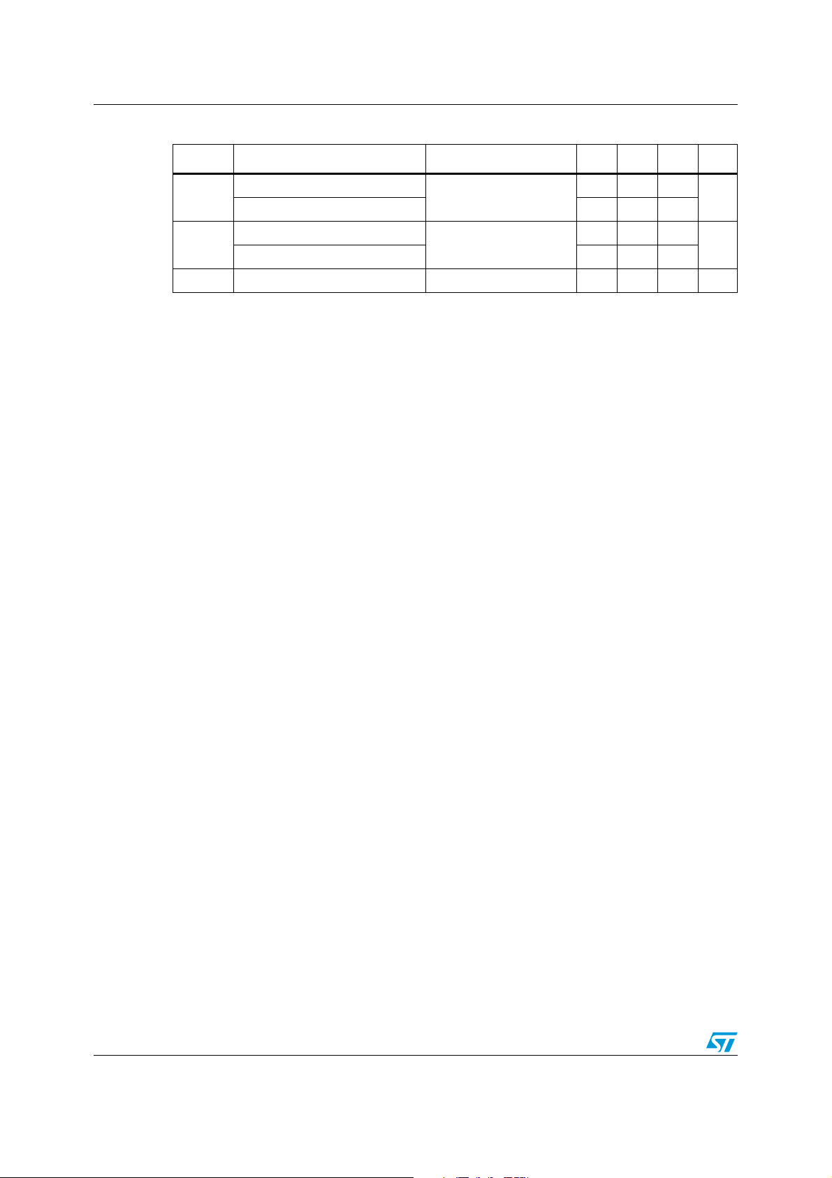
Table 6. Electrical specifications
Symbol Parameter Condition Min Typ Max Unit
I
q
I
qSTBY
V
OS
I
OCP
8/28 Doc ID 16107 Rev 8
Total quiescent current No LC filter, no load - 40 60 mA
Quiescent current in standby - - 1 10 µA
Output offset voltage
Overcurrent protection threshold RL = 0 Ω 67- A
= R3 = 39 kΩ, C8 = 100 nF, f = 1 kHz, GV = 25.6 dB
OSC
Play mode -100 - 100
Mute mode -60 - 60
mV
Page 9

TDA7498 Electrical specifications
Table 6. Electrical specifications (continued)
Symbol Parameter Condition Min Typ Max Unit
T
R
V
V
R
P
P
P
j
i
OVP
UVP
dsON
o
o
D
Junction temperature at thermal
shutdown
Input resistance Differential input 48 60 - kΩ
Overvoltage protection threshold - 42 43 - V
Undervoltage protection
threshold
Power transistor on resistance
Output power
Output power RL = 8 Ω, THD = 10% - 80 - W
Dissipated power
η Efficiency P
THD Total harmonic distortion P
G
ΔG
C
V
V
T
Closed-loop gain
Gain matching - -1 - 1 dB
Crosstalk f = 1 kHz, Po = 1 W 5070- dB
eN Total input noise
SVRR Supply voltage rejection ratio
, T
T
r
f
SW
f
SWR
V
inH
V
inL
Rise and fall times - - 50 - ns
f
Switching frequency Internal oscillator 290 310 330 kHz
Output switching frequency
range
Digital input high (H)
Digital input low (L) - - 0.8
- - 150 - °C
- --8V
High side - 0.2 -
Ω
Low side - 0.2 -
THD = 10% - 100 -
W
THD = 1% - 78 -
= 100 W + 100 W,
P
o
THD = 10%
= 100 W + 100 W - 90 - %
o
= 1 W - 0.1 - %
o
-20-W
GAIN0 = L, GAIN1 = L 24.6 25.6 26.6
GAIN0 = L, GAIN1 = H 30.6 31.6 32.6
dB
GAIN0 = H, GAIN1 = L 34.1 35.1 36.1
GAIN0 = H, GAIN1 = H 36.6 37.6 38.6
A Curve, G
= 20 dB - 15 -
V
µV
f = 22 Hz to 22 kHz - 25 50
fr = 100 Hz, Vr = 0.5 Vpp,
= 10 µF
C
SVR
With internal oscillator
With external oscillator
-70-dB
(1)
250 - 400
(2)
250 - 400
kHz
2.3 - -
-
V
Doc ID 16107 Rev 8 9/28
Page 10
Electrical specifications TDA7498
Table 6. Electrical specifications (continued)
Symbol Parameter Condition Min Typ Max Unit
V
STBY
Pin STBY voltage low (L) - - 0.5
Pin MUTE voltage high (H)
V
Pin STBY voltage high (H)
MUTE
A
MUTE
1. fSW = 106 / ((16 * R
2. f
SW
Pin MUTE voltage low (L) - - 0.8
Mute attenuation V
= f
/ 2 with the external oscillator.
SYNCLK
+ 182) * 4) kHz, f
OSC
-
-
= L, V
MUTE
= 2 * fSW with R3 = 39 kΩ (see Figure 19.).
SYNCLK
= H - 70 - dB
STBY
2.7 - V
2.5 - V
10/28 Doc ID 16107 Rev 8
Page 11
3 Characterizations
3.1 Test circuit
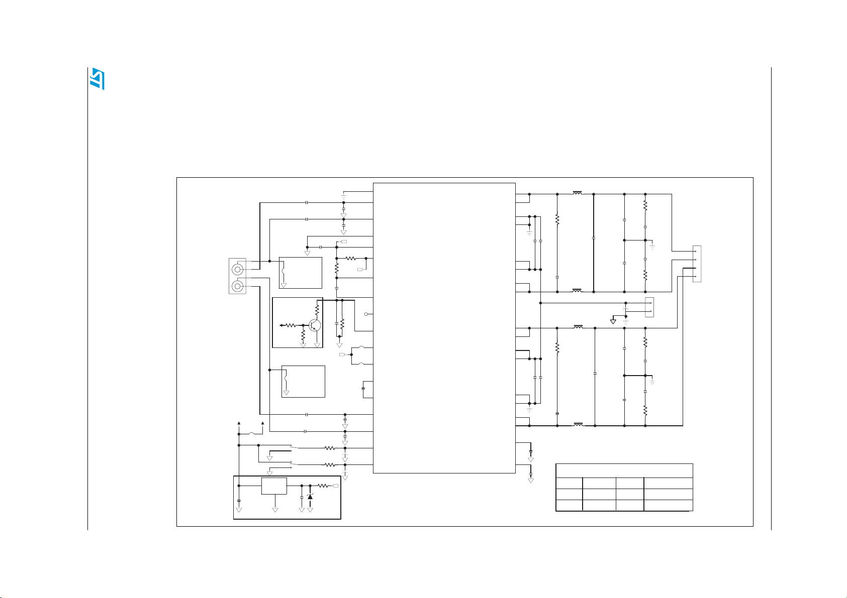
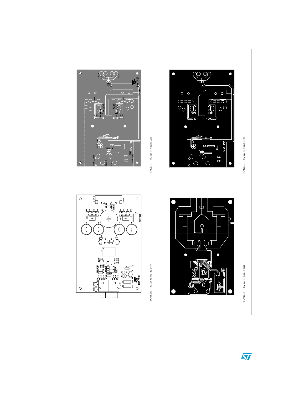
Figure 3 shows the test circuit with which the characterization curves, shown in the next sections, were measured. Figure 4 shows
the PCB layout.
Figure 3. Test circuit for characterizations
J1
Doc ID 16107 Rev 8 11/28
INPUT
3V3 FS
3V3
C29
2.2uF
3
4
1
2
J4
OUT
L-
L+
R-
R+
L4931CZ3
1
1uF
1uF
For
J7
Single-Ended
Input
FREQUENCY SHIFT
Q1
KTC3875(S)
180K
R13
FS
47k
R14
100k
J8
Single-Ended
Input
C11
1uF
C12
1uF
S2
MUTE
1
2
3
S1
STBY
1
2
3
IN
IC2
3
3
C9
GND
2
100nF
3V3 POWER SUPPL
TDA7498 Characterizations
22R
C30
1uF
R5
C31
C21
R6
C27
L4
22uH
*
L3
22uH
*
L1
22uH
*
L2
22uH
*
LC FILTER COMPONENTS
Load
L1,L2,L3,L4
6 ohm
22 uH
8 ohm
22 uH 470 nF
*
C28
220nF
C26
*
680nF
*
C24
220nF
2200uF
+
C23
50V
C18
*
220nF
C20
*
680nF
C22
*
220nF
C20,C26 C18,C22,C24,C28
680 nF
R15
8R
C40
220nF
C41
220nF
1
2
J2
R17
C42
220nF
C43
220nF
R18
8R
R16
8R
8R
VCC
GND
220 nF
220 nF
J3
OUTPUT
Load = 6 ohm
L+
1
L-
2
R-
3
R+
4
1
VDDS
R1
100k
DIAG
R3
100nF
C3
1nF
C4
1nF
C10
C13
1nF
C14
1nF
C15
2.2uF
16V
C7
2.2uF
16V
SUB_GND
22
INPA
23
INNA
27
SGND
26
VDDS
28
DIAG
19
VDDPW
18
PGND
25
SYNCLK
24
ROSC
30
J5
GAIN0
31
GAIN1
J6
35
SVCC
36
VSS
32
INPB
33
INNB
21
MUTE
20
STBY
IC1
TDA7498
TDA7498
CLASS-D AMPLIFIER
C1
C2
C5
100nF
R7
22R
C6
100nF
R9
3
C8
100nF
1
For
2
18V
Y
39K
VDDS
R4
+
120k
R2
+
33k
R8
VCC
6.8k
D1
OUTPA
OUTPA
PGNDA
PGNDA
PVCCA
PVCCA
OUTNA
OUTNA
OUTPB
OUTPB
PVCCB
PVCCB
PGNDB
PGNDB
OUTNB
OUTNB
VREF
SVR
16
17
14
15
100nF
12
13
10
11
7
6
100nF
9
8
C25
330pF
3
2
22R
C19
1uF
5
4
330pF
34
C17
10uF
29
10V
C16
10uF
10V
Page 12
Characterizations TDA7498
Figure 4. Test board
12/28 Doc ID 16107 Rev 8
Page 13
TDA7498 Characterizations
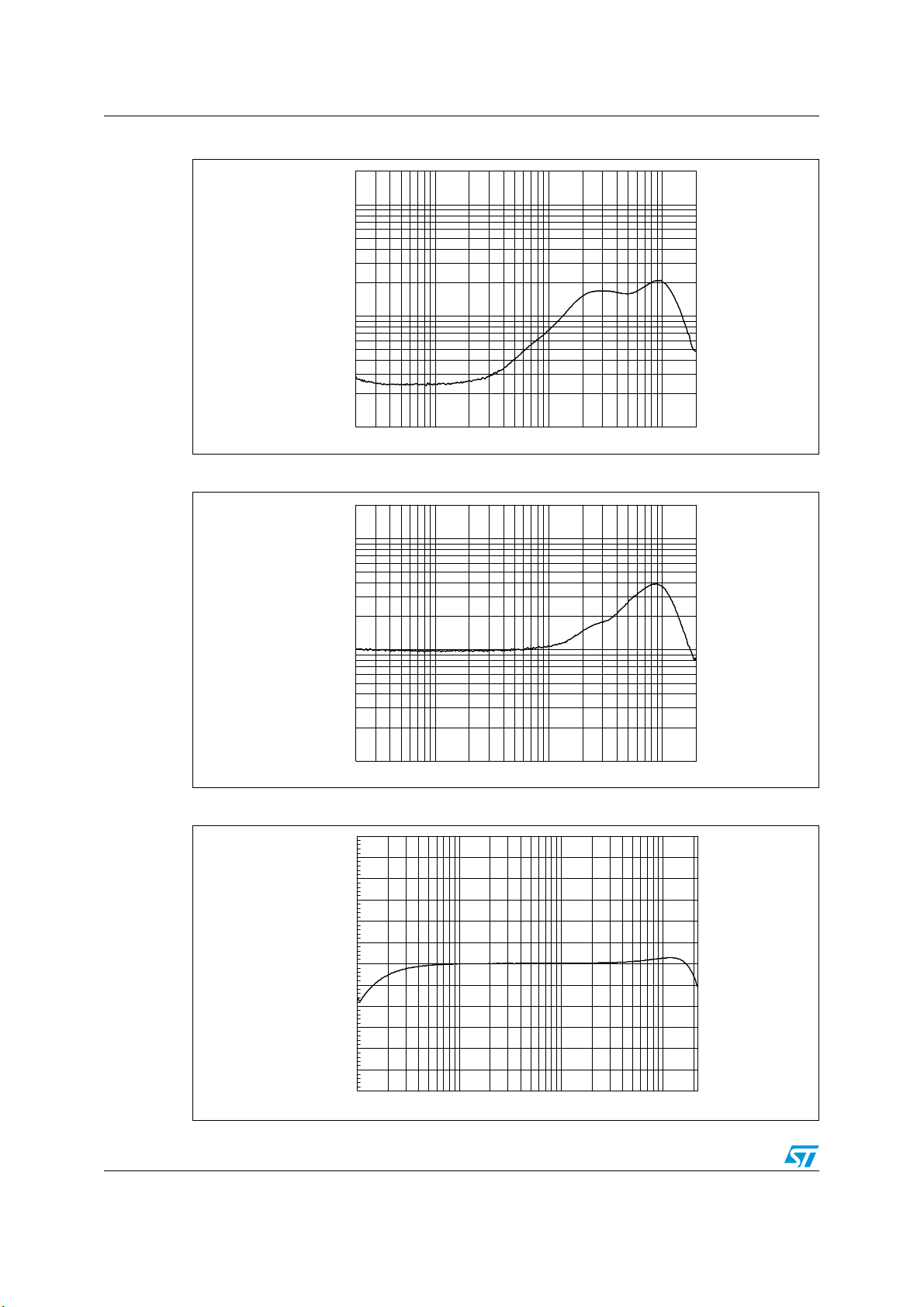
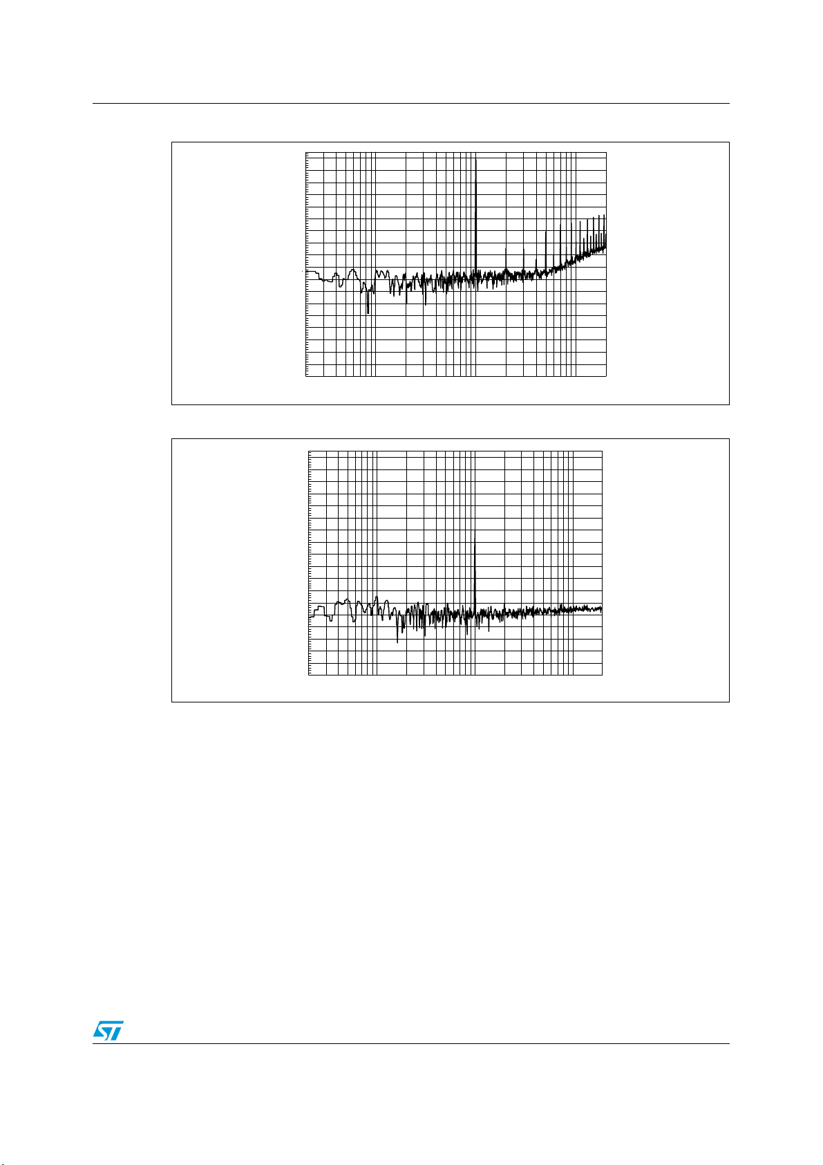
3.2 Characterization curves
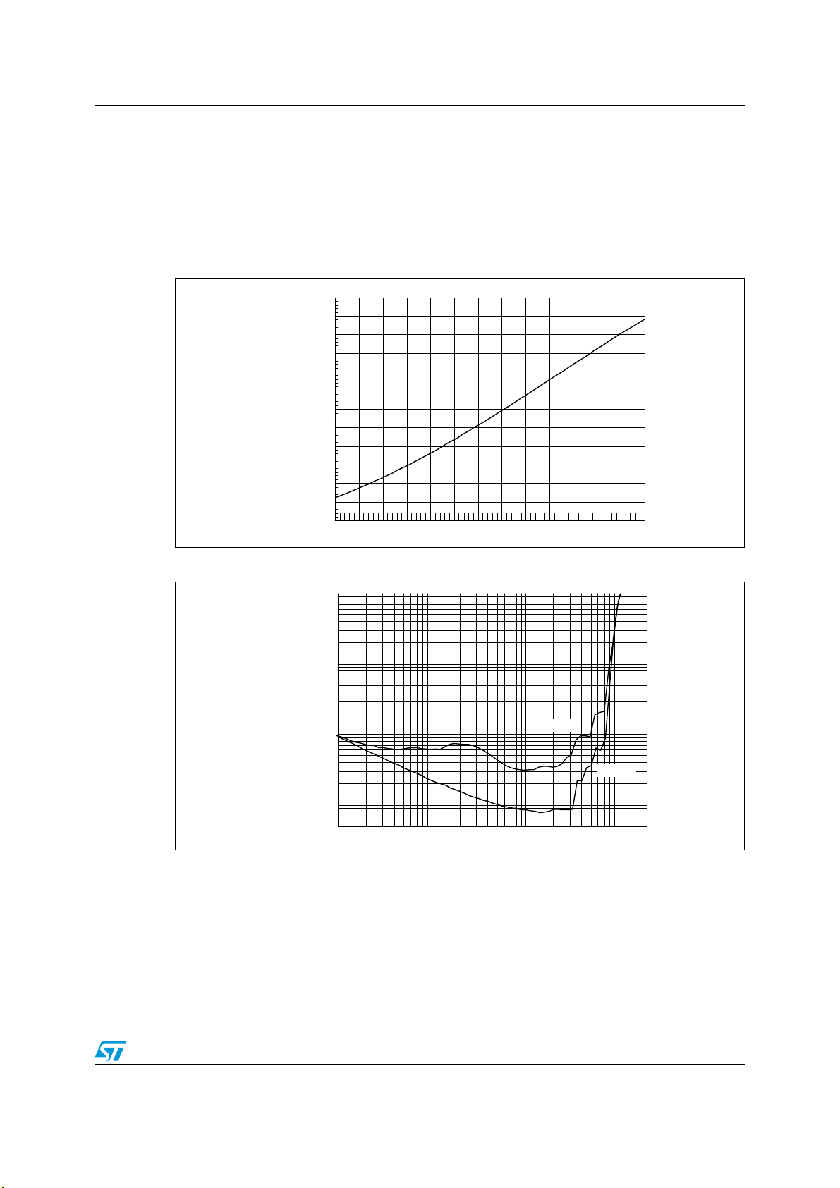
Unless otherwise stated the measurements were made under the following conditions:
V
= 36 V, f = 1 kHz, GV = 25.6 dB, R
CC
3.2.1 For RL = 6 Ω
Figure 5. Output power (THD = 10%) vs. supply voltage
Output power (W)
120
110
100
90
80
70
60
50
40
30
20
10
= 39 kΩ, C
OSC
= 100 nF, Tamb = 25 °C
OSC
+10 +36+12 +14 +16 +18 +20 +22 +24 +26 +28 +30+32+34
Figure 6. THD vs. output power
10
5
THD+N (%)
2
1
0.5
0.2
0.1
0.05
0.02
0.01
0.005
100m 200200m 500m 1 2 5 10 20 50 100
Supply voltage (V)
f = 1 kHz
f = 100 Hz
Output power (W)
Doc ID 16107 Rev 8 13/28
Page 14
Characterizations TDA7498
Figure 7. THD vs. frequency (1 W)
2
1
THD+N (%)
0.5
0.2
0.1
0.05
0.02
0.01
20 20k50 100 200 500 1k 2k 5k 10k
Frequency (Hz)
Figure 8. THD vs. frequency (100 mW)
2
1
THD+N (%)
0.5
0.2
0.1
0.05
0.02
0.01
20 20k50 100 200 500 1k 2k 5k 10k
Figure 9. Frequency response
+3
+2.5
Ampl (dB)
+2
+1.5
+1
+0.5
+0
-0.5
-1
-1.5
-2
-2.5
-3
10 20k20 50 100 200 500 1k 2k 5k 10k
Frequency (Hz)
Frequency (Hz)
14/28 Doc ID 16107 Rev 8
Page 15
TDA7498 Characterizations
Figure 10. FFT performance (0 dBFS)
+0
-10
-20
FFT (dB)
-30
-40
-50
-60
-70
-80
-90
-100
-110
-120
-130
-140
-150
-160
-170
-180
20 20k50 100 200 500 1k 2k 5k 10k
Frequency (Hz)
Figure 11. FFT performance (-60 dBFS)
+0
-10
-20
FFT (dB)
-30
-40
-50
-60
-70
-80
-90
-100
-110
-120
-130
-140
-150
-160
-170
-180
20 20k50 100 200 500 1k 2k 5k 10k
Frequency (Hz)
Doc ID 16107 Rev 8 15/28
Page 16
Characterizations TDA7498
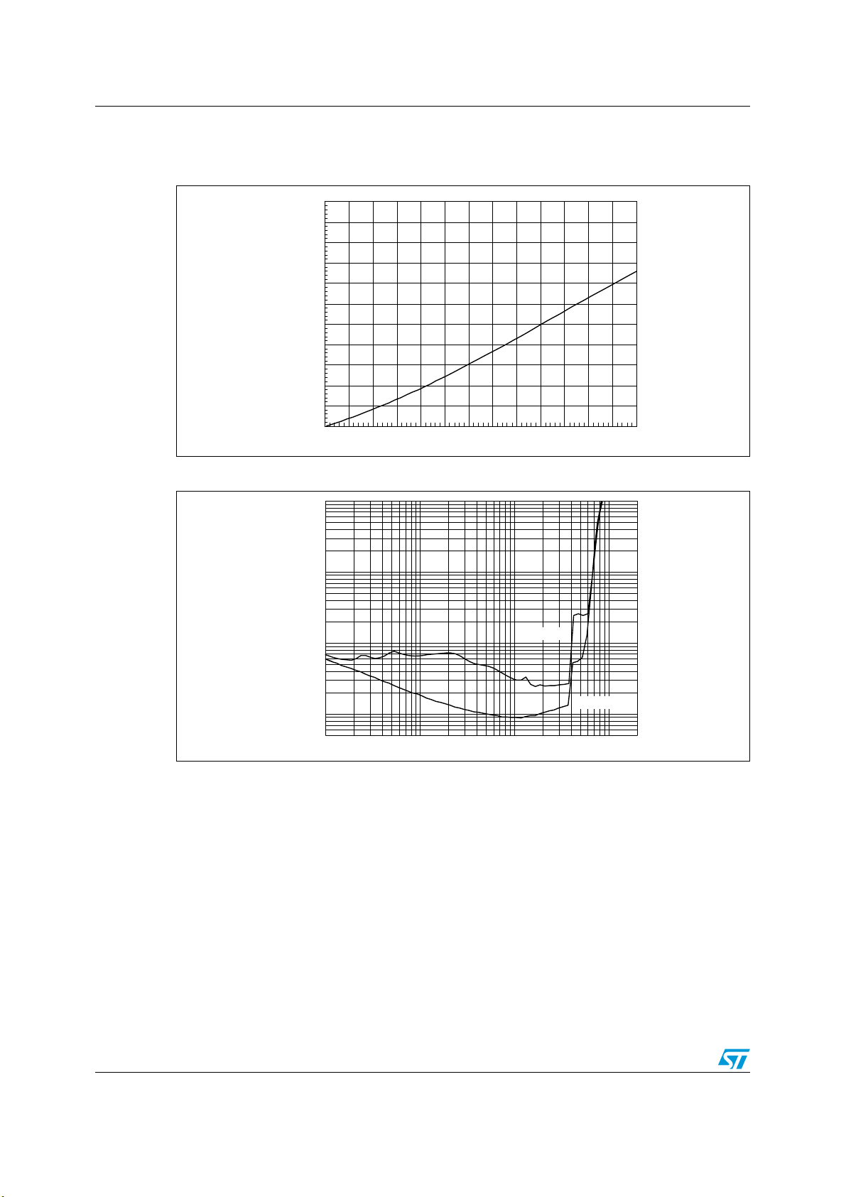
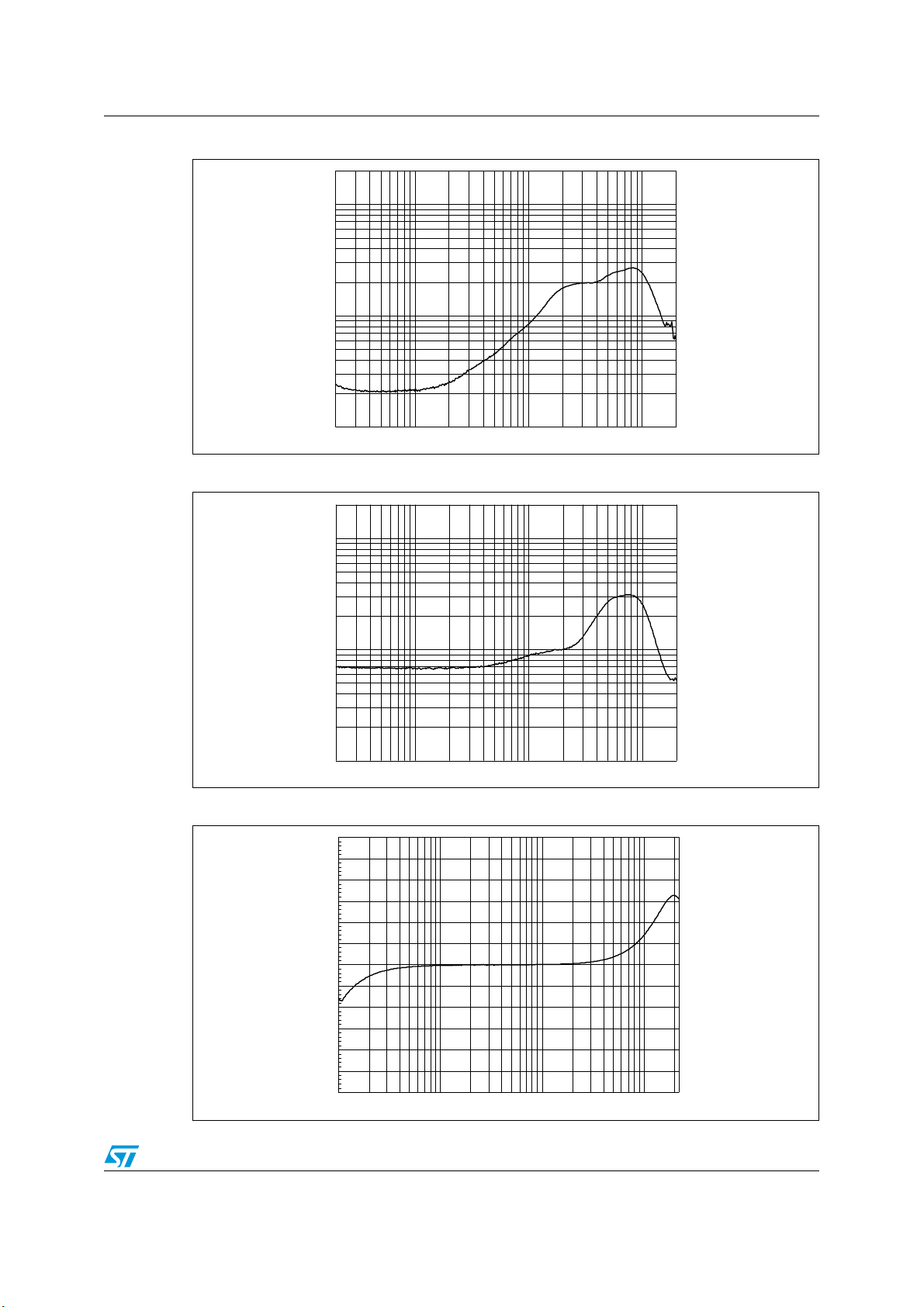
3.2.2 For RL = 8 Ω
Figure 12. Output power (THD = 10%) vs. supply voltage
120
Output power (W)
Figure 13. THD vs. output power
110
100
90
80
70
60
50
40
30
20
10
+10 +36+12 +14 +16 +18 +20 +22 +24 +26 +28 +30+32+34
10
5
THD+N (%)
2
1
0.5
Supply voltage (V)
0.2
0.1
0.05
0.02
0.01
0.005
100m 200200m 500m 1 2 5 10 20 50 100
Output power (W)
f = 1 kHz
f = 100 Hz
16/28 Doc ID 16107 Rev 8
Page 17
TDA7498 Characterizations
Figure 14. THD vs. frequency (1 W)
2
1
THD+N (%)
0.5
0.2
0.1
0.05
0.02
0.01
20 20k50 100 200 500 1k 2k 5k 10k
Frequency (Hz)
Figure 15. THD vs. frequency (100 mW)
2
1
THD+N (%)
0.5
0.2
0.1
0.05
0.02
0.01
20 20k50 100 200 500 1k 2k 5k 10k
Figure 16. Frequency response
+3
+2.5
Ampl (dB)
+2
+1.5
+1
+0.5
+0
-0.5
-1
-1.5
-2
-2.5
-3
10 20k20 50 100 200 500 1k 2k 5k 10k
Frequency (Hz)
Frequency (Hz)
Doc ID 16107 Rev 8 17/28
Page 18
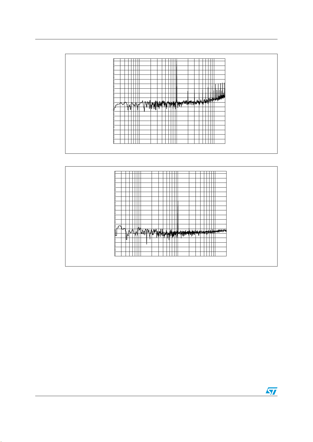
Characterizations TDA7498
Figure 17. FFT performance (0 dB)
))7G%
N N N N N
)UHTXHQF\+]
Figure 18. FFT performance (-60 dB)
+0
-10
-20
FFT (dB)
-30
-40
-50
-60
-70
-80
-90
-100
-110
-120
-130
-140
-150
-160
-170
-180
20 20k50 100 200 500 1k 2k 5k 10k
Frequency (Hz)
18/28 Doc ID 16107 Rev 8
Page 19
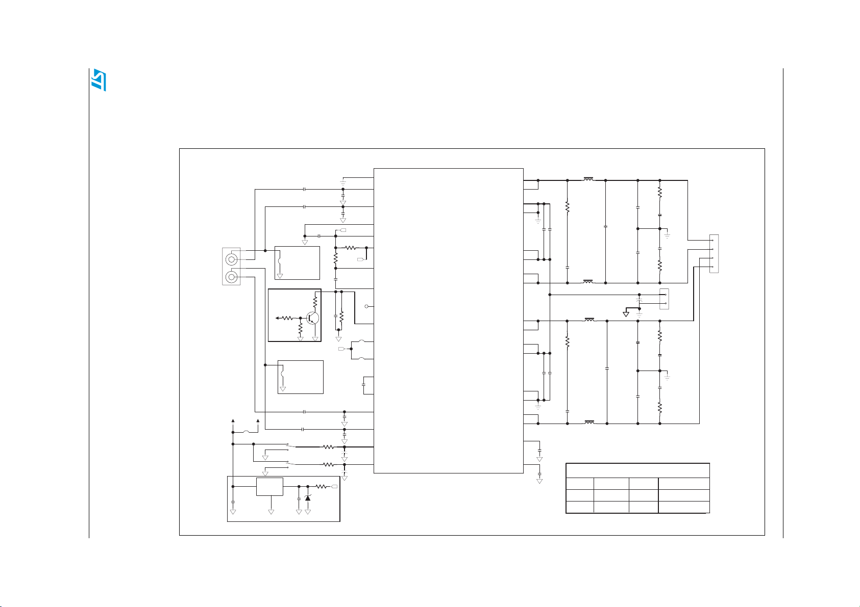
4 Applications information
4.1 Applications circuit
Figure 19. Applications circuit for 6- or 8-Ω speakers
TDA7498 Applications information
Doc ID 16107 Rev 8 19/28
J1
INPUT
L-
3
L+
4
R-
1
R+
2
3V3 FS
3V3
J4
OUT
C29
2.2uF
FREQUENCY SHIFT
KTC3875(S)
FS
S2
S1
IC2
L4931CZ3
1
GND
2
3V3 POWER SUPPL
J7
Single-Ended
Q1
R13
47k
R14
100k
J8
Single-Ended
MUTE
1
3
STBY
1
3
IN
3
3
C9
100nF
1uF
For
Input
C11
1uF
C12
1uF
2
2
C1
1uF
C2
180K
1
For
Input
R6
C27
L4
22uH
*
L3
22uH
*
L1
22uH
*
L2
22uH
*
LC FILTER COMPONENTS
Load
L1,L2,L3,L4
6 ohm
22 uH
8 ohm
22 uH 470 nF
*
C28
220nF
C26
*
680nF
*
C24
220nF
2200uF
+
C23
50V
C18
*
220nF
C20
*
680nF
C22
*
220nF
C20,C26 C18,C22,C24,C28
680 nF
R15
8R
C40
220nF
C41
220nF
R16
1
2
J2
R17
8R
C42
220nF
C43
220nF
R18
8R
8R
VCC
GND
220 nF
220 nF
J3
OUTPUT
Load = 6 ohm
L+
1
L-
2
R-
3
R+
4
1
SUB_GND
22
INPA
C3
1nF
23
INNA
C4
1nF
27
SGND
+
+
100k
DIAG
R3
39K
VDDS
R1
C10
100nF
C13
1nF
C14
1nF
C15
2.2uF
16V
C7
2.2uF
16V
26
VDDS
28
DIAG
19
VDDPW
18
PGND
25
SYNCLK
24
ROSC
30
J5
GAIN0
31
GAIN1
J6
35
SVCC
36
VSS
32
INPB
33
INNB
21
MUTE
20
STBY
IC1
TDA7498
TDA7498
CLASS-D AMPLIFIER
C5
100nF
R7
22R
C6
100nF
R9
3
C8
100nF
2
VDDS
R4
120k
R2
33k
R8
VCC
6.8k
D1
18V
Y
OUTPA
OUTPA
PGNDA
PGNDA
PVCCA
PVCCA
OUTNA
OUTNA
OUTPB
OUTPB
PVCCB
PVCCB
PGNDB
PGNDB
OUTNB
OUTNB
VREF
SVR
16
17
14
15
100nF
12
13
10
11
3
2
7
6
100nF
5
4
9
8
34
29
C25
C19
C17
10uF
10V
C16
10uF
10V
22R
C30
1uF
330pF
R5
22R
C31
1uF
C21
330pF
Page 20
Applications information TDA7498
4.2 Mode selection
The three operating modes of the TDA7498 are set by the two inputs, STBY (pin 20) and
MUTE (pin 21).
● Standby mode: all circuits are turned off, very low current consumption.
● Mute mode: inputs are connected to ground and the positive and negative PWM
outputs are at 50% duty cycle.
● Play mode: the amplifiers are active.
The protection functions of the TDA7498 are enabled by pulling down the voltages of the
STBY and MUTE inputs shown in Figure 20. The input current of the corresponding pins
must be limited to 200 µA.
Table 7. Mode settings
Mode STBY MUTE
Standby L
Mute H
Play H H
1. Drive levels defined in Table 6: Electrical specifications on page 8
(1)
(1)
X (don’t care)
L
Figure 20. Standby and mute circuits
0 V
0 V
Standby
3.3 V
Mute
3.3 V
R2
30 kΩ
R4
30 kΩ
C7
2.2 µF
C15
2.2 µF
STBY
TDA7498
MUTE
Figure 21. Turn on/off sequence for minimizing speaker “pop”
VCC
0
STBY
0
MUTE
0
Input
0
Output
0
Standby Mute Play Mute Standby
I
q
0
t
t
t
t
t
t
20/28 Doc ID 16107 Rev 8
Page 21
TDA7498 Applications information
4.3 Gain setting
The gain of the TDA7498 is set by the two inputs, GAIN0 (pin 30) and GAIN1 (pin31).
Internally, the gain is set by changing the feedback resistors of the amplifier.
Table 8. Gain settings
GAIN0 GAIN1 Nominal gain, Gv (dB)
LL25.6
LH31.6
HL 35.6
HH37.6
4.4 Input resistance and capacitance
The input impedance is set by an internal resistor Ri = 60 kΩ (typical). An input capacitor
(Ci) is required to couple the AC input signal.
The equivalent circuit and frequency response of the input components are shown in
Figure 22. For Ci = 470 nF the high-pass filter cutoff frequency is below 20 Hz:
fC = 1 / (2 * π * Ri * Ci)
Figure 22. Input circuit and frequency response
Input
signal
Input
Ci
pin
Ri
Rf
Doc ID 16107 Rev 8 21/28
Page 22
Applications information TDA7498
4.5 Internal and external clocks
The clock of the class-D amplifier can be generated internally or can be driven by an
external source.
If two or more class-D amplifiers are used in the same system, it is recommended that all
devices operate at the same clock frequency. This can be implemented by using one
TDA7498 as master clock, while the other devices are in slave mode, that is, externally
clocked. The clock interconnect is via pin SYNCLK of each device. As explained below,
SYNCLK is an output in master mode and an input in slave mode.
4.5.1 Master mode (internal clock)
Using the internal oscillator, the output switching frequency, fSW, is controlled by the
resistor, R
fSW = 106 / ((R
where R
In master mode, pin SYNCLK is used as a clock output pin whose frequency is:
f
SYNCLK
For master mode to operate correctly then resistor R
below in Ta bl e 9 .
, connected to pin ROSC:
OSC
* 16 + 182) * 4) kHz
OSC
is in kΩ.
OSC
= 2 * fSW
must be less than 60 kΩ as given
OSC
4.5.2 Slave mode (external clock)
In order to accept an external clock input the pin ROSC must be left open, that is, floating.
This forces pin SYNCLK to be internally configured as an input as given in Ta bl e 9 .
The output switching frequency of the slave devices is:
f
= f
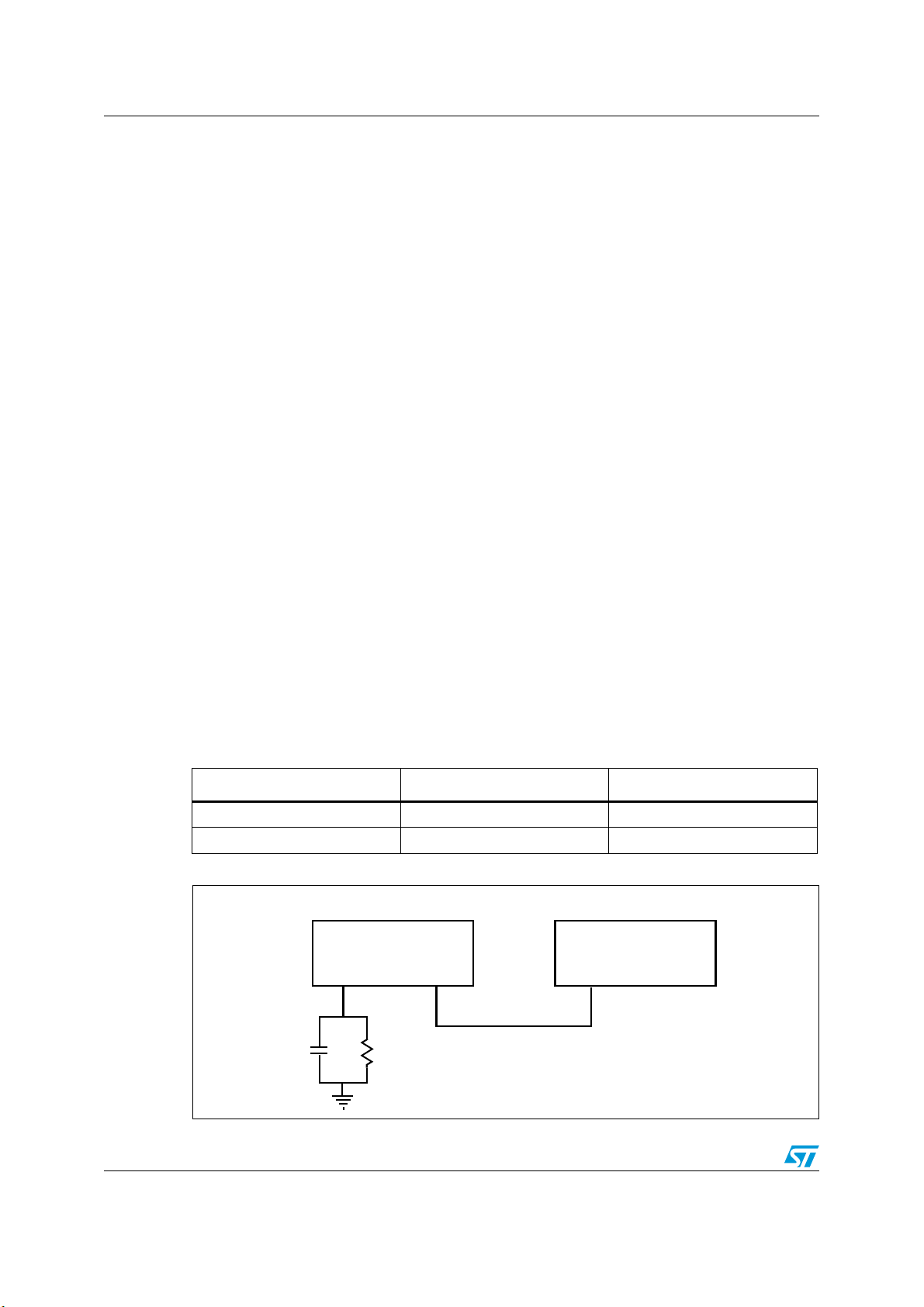
SW
SYNCLK
Table 9. How to set up SYNCLK
Master R
Slave Floating (not connected) Input
Figure 23. Master and slave connection
/ 2
Mode ROSC SYNCLK
OSC
Master Slave
TDA7498
ROSC SYNCLK
Cosc
100 nF
Rosc
39 kΩ
< 60 kΩ Output
TDA7498
SYNCLK ROSC
Output
Input
22/28 Doc ID 16107 Rev 8
Page 23
TDA7498 Applications information
4.6 Output low-pass filter
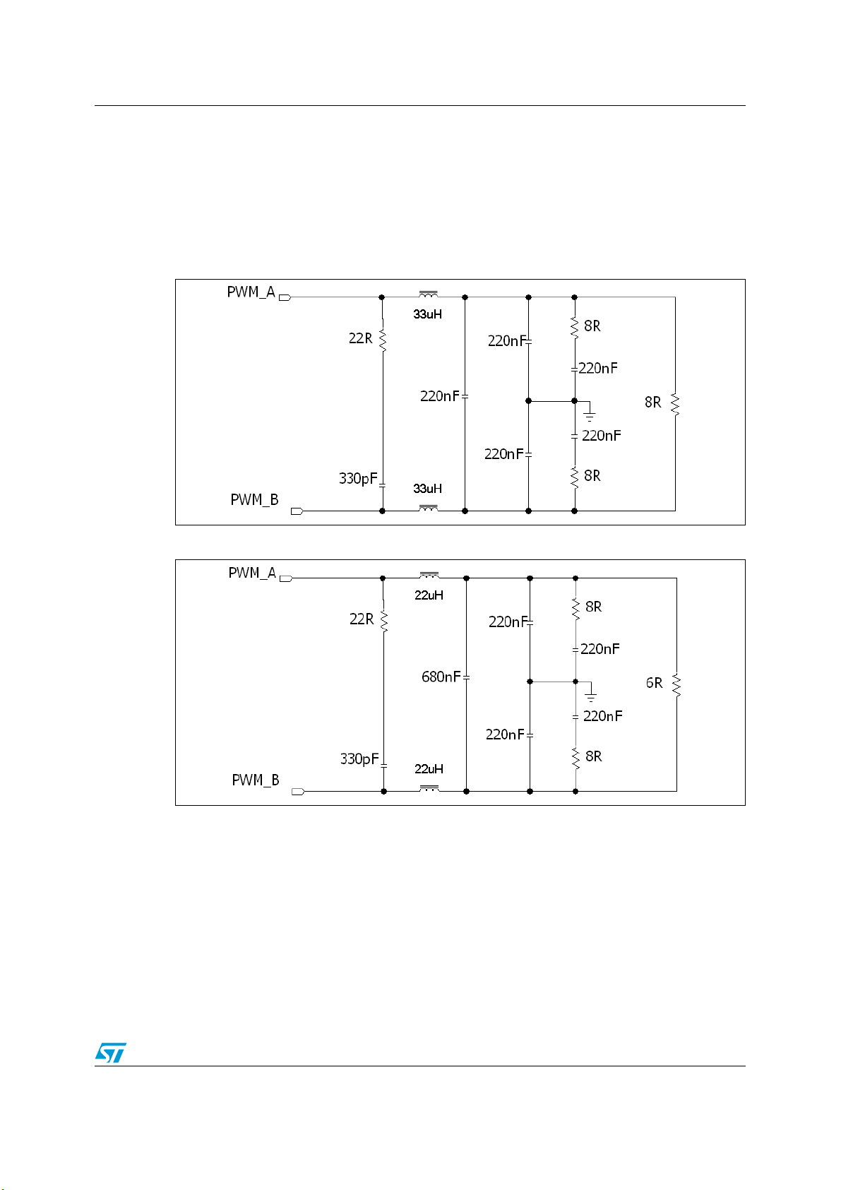
To avoid EMI problems, it may be necessary to use a low-pass filter before the speaker. The
cutoff frequency should be larger than 22 kHz and much lower than the output switching
frequency. It is necessary to choose the L and C component values depending on the
loud-speaker impedance. Some typical values, which give a cutoff frequency of 27 kHz, are
shown in Figure 24 and Figure 25 below.
Figure 24. Typical LC filter for a 8-Ω speaker
Figure 25. Typical LC filter for a 6-Ω speaker
Doc ID 16107 Rev 8 23/28
Page 24
Applications information TDA7498
4.7 Protection functions
The TDA7498 is fully protected against overvoltages, undervoltages, overcurrents and
thermal overloads as explained here.
Overvoltage protection (OVP)
If the supply voltage exceeds the value for V
given in Table 6: Electrical specifications on
OVP
page 8 the overvoltage protection is activated which forces the outputs to the
high-impedance state. When the supply voltage falls back to within the operating range the
device restarts.
Undervoltage protection (UVP)
If the supply voltage drops below the value for V
specifications on page 8 the undervoltage protection is activated which forces the outputs to
the high-impedance state. When the supply voltage recovers to within the operating range
the device restarts.
given in Table 6: Electrical
UVP
Overcurrent protection (OCP)
If the output current exceeds the value for I
page 8 the overcurrent protection is activated which forces the outputs to the
high-impedance state. Periodically, the device attempts to restart. If the overcurrent
condition is still present then the OCP remains active. The restart time, T
by the R-C components connected to pin STBY.
given in Table 6: Electrical specifications on
OCP
, is determined
OC
Thermal protection (OTP)
If the junction temperature, Tj, reaches 145 °C (nominally), the device goes to mute mode
and the positive and negative PWM outputs are forced to 50% duty cycle. If the junction
temperature reaches the value for T
device shuts down and the output is forced to the high-impedance state. When the device
cools sufficiently the device restarts.
given in Table 6: Electrical specifications on page 8 the
j
4.8 Diagnostic output
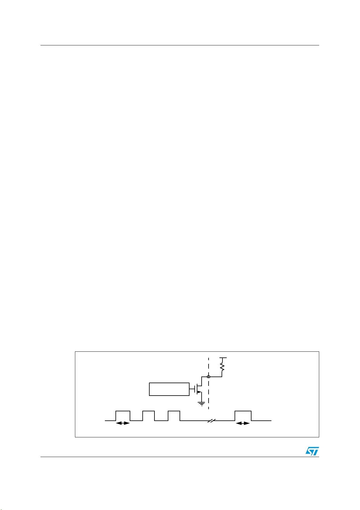
The output pin DIAG is an open drain transistor. When any protection is activated it switches
to the high-impedance state. The pin can be connected to a power supply (< 39 V) by a
pull-up resistor whose value is limited by the maximum sinking current (200 µA) of the pin.
Figure 26. Behavior of pin DIAG for various protection conditions
TDA7498
Protection logic
VDD
Overcurrent
protection
24/28 Doc ID 16107 Rev 8
Restart
DIAG
VDD
R1
OV, UV, OT
protection
Restart
Page 25
TDA7498 Package mechanical data
5 Package mechanical data
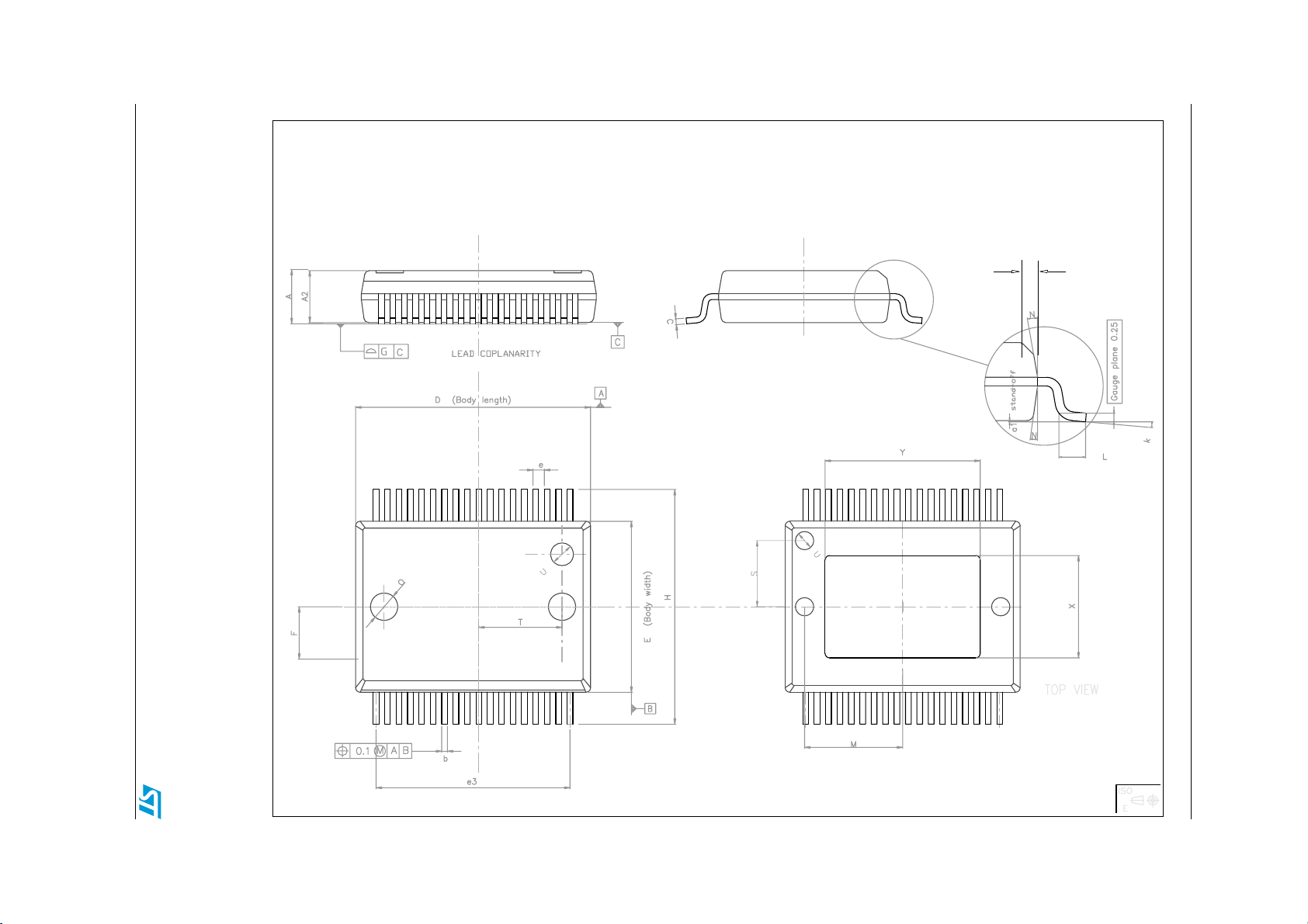
The TDA7498 comes in a 36-pin PowerSSO package with exposed pad up.
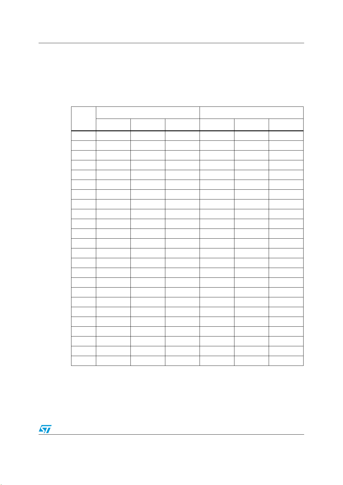
Figure 27 shows the package outline and Ta bl e 10 gives the dimensions.
Table 10. PowerSSO36 EPU dimensions
Dimensions in mm Dimensions in inches
Symbol
Min Typ Max Min Typ Max
A 2.15 - 2.45 0.085 - 0.096
A2 2.15 - 2.35 0.085 - 0.093
a1 0 - 0.10 0 - 0.004
b 0.18 - 0.36 0.007 - 0.014
c 0.23 - 0.32 0.009 - 0.013
D 10.10 - 10.50 0.398 - 0.413
E 7.40 - 7.60 0.291 - 0.299
e - 0.5 - - 0.020 -
e3 - 8.5 - - 0.335 -
F - 2.3 - - 0.091 -
G- - 0.10 - - 0.004
H 10.10 - 10.50 0.398 - 0.413
h- - 0.40 - - 0.016
k 0 - 8 degrees - - 8 degrees
L 0.60 - 1.00 0.024 - 0.039
M - 4.30 - - 0.169 -
N - - 10 degrees - - 10 degrees
O - 1.20 - - 0.047 -
Q - 0.80 - - 0.031 -
S - 2.90 - - 0.114 -
T - 3.65 - - 0.144 -
U - 1.00 - - 0.039 -
X 4.10 - 4.70 0.161 - 0.185
Y 4.90 - 7.10 0.193 - 0.280
In order to meet environmental requirements, ST offers these devices in different grades of
ECOPACK
specifications, grade definitions and product status are available at: www.st.com.
ECOPACK
®
packages, depending on their level of environmental compliance. ECOPACK®
®
is an ST trademark.
Doc ID 16107 Rev 8 25/28
Page 26
26/28 Doc ID 16107 Rev 8
Figure 27. PowerSSO36 EPU outline drawing
h x 45°
Package mechanical data TDA7498
Page 27
TDA7498 Revision history
6 Revision history
Table 11. Document revision history
Date Revision Changes
11-Aug-2009 1 Initial release.
Updated supply voltage range on page 1
27-Aug-2009 2
23-Oct-2009 3
30-Jun-2010 4
27-Jan-2011 5 Updated applications circuit in Figure 19 on page 19.
Updated package exposed pad dimension Y (Min) in Table 10 on
page 25.
Updated first feature on page 1
Updated order code name in Table 1 on page 1
Updated Table 5: Electrical specifications on page 8
Updated Section 3.2: Characterization curves on page 13
Removed tables for standby, mute and gain after Figure 19 on
page 19.
Removed datasheet preliminary status, updated features list and
updated Device summary table on page 1
Added Table 5: Recommended operating conditions on page 8 with
updated minimum supply voltage.
11-Feb-2011 6 Updated test circuit for characterizations in Figure 3 on page 11.
29-Mar-2011 7 Updated I
12-Sep-2011 8 Updated OUTNA in Table 2: Pin description list
in Table 6: Electrical specifications.
OCP
Doc ID 16107 Rev 8 27/28
Page 28

TDA7498
Please Read Carefully:
Information in this document is provided solely in connection with ST products. STMicroelectronics NV and its subsidiaries (“ST”) reserve the
right to make changes, corrections, modifications or improvements, to this document, and the products and services described herein at any
time, without notice.
All ST products are sold pursuant to ST’s terms and conditions of sale.
Purchasers are solely responsible for the choice, selection and use of the ST products and services described herein, and ST assumes no
liability whatsoever relating to the choice, selection or use of the ST products and services described herein.
No license, express or implied, by estoppel or otherwise, to any intellectual property rights is granted under this document. If any part of this
document refers to any third party products or services it shall not be deemed a license grant by ST for the use of such third party products
or services, or any intellectual property contained therein or considered as a warranty covering the use in any manner whatsoever of such
third party products or services or any intellectual property contained therein.
UNLESS OTHERWISE SET FORTH IN ST’S TERMS AND CONDITIONS OF SALE ST DISCLAIMS ANY EXPRESS OR IMPLIED
WARRANTY WITH RESPECT TO THE USE AND/OR SALE OF ST PRODUCTS INCLUDING WITHOUT LIMITATION IMPLIED
WARRANTIES OF MERCHANTABILITY, FITNESS FOR A PARTICULAR PURPOSE (AND THEIR EQUIVALENTS UNDER THE LAWS
OF ANY JURISDICTION), OR INFRINGEMENT OF ANY PATENT, COPYRIGHT OR OTHER INTELLECTUAL PROPERTY RIGHT.
UNLESS EXPRESSLY APPROVED IN WRITING BY TWO AUTHORIZED ST REPRESENTATIVES, ST PRODUCTS ARE NOT
RECOMMENDED, AUTHORIZED OR WARRANTED FOR USE IN MILITARY, AIR CRAFT, SPACE, LIFE SAVING, OR LIFE SUSTAINING
APPLICATIONS, NOR IN PRODUCTS OR SYSTEMS WHERE FAILURE OR MALFUNCTION MAY RESULT IN PERSONAL INJURY,
DEATH, OR SEVERE PROPERTY OR ENVIRONMENTAL DAMAGE. ST PRODUCTS WHICH ARE NOT SPECIFIED AS "AUTOMOTIVE
GRADE" MAY ONLY BE USED IN AUTOMOTIVE APPLICATIONS AT USER’S OWN RISK.
Resale of ST products with provisions different from the statements and/or technical features set forth in this document shall immediately void
any warranty granted by ST for the ST product or service described herein and shall not create or extend in any manner whatsoever, any
liability of ST.
ST and the ST logo are trademarks or registered trademarks of ST in various countries.
Information in this document supersedes and replaces all information previously supplied.
The ST logo is a registered trademark of STMicroelectronics. All other names are the property of their respective owners.
© 2011 STMicroelectronics - All rights reserved
STMicroelectronics group of companies
Australia - Belgium - Brazil - Canada - China - Czech Republic - Finland - France - Germany - Hong Kong - India - Israel - Italy - Japan -
Malaysia - Malta - Morocco - Philippines - Singapore - Spain - Sweden - Switzerland - United Kingdom - United States of America
www.st.com
28/28 Doc ID 16107 Rev 8
 Loading...