

Page 1
TDA7476
CAR RADIO DIAGNOSTIC PROCESSOR
PRELIMINARY DATA
WIDEOPERATINGVOLTAGERANGE
ST-BYFUNCTION (C-MOS)
LOW QUIESCENT ST-BY CURRENT CON-
SUMPTION
I2C BUS INTERFACE WITH 2 EXTERNALLY
SELECTABLEADDRESSES
UP TO 5 BTL EQUIVALENT INPUTS FOR
FAULT DETECTION IN THE AUDIO CHANNELS
- shortto GND
- shortto Vs
- shortacross the load (at turn-on)
- openload (at turn-on)
2 AUX INPUTS FOR FAULT DETECTION IN
THE ANTENNA AND BOOSTERS SUPPLY
LINE
- shortto GND
- openload
WARNING PIN FUNCTION (interrupt facility)
ACTIVATED IN THE FOLLOWING CONDITION:
- audiochannelshorted to V
S
- audiochannelshorted to GND
- aux input shorted to GND
NOISEFREE DIAGNOSTICSOPERATION
PROTETCTORS
LOADDUMP VOLTAGE
MULTIPOWER BCD TECHNOLOGY
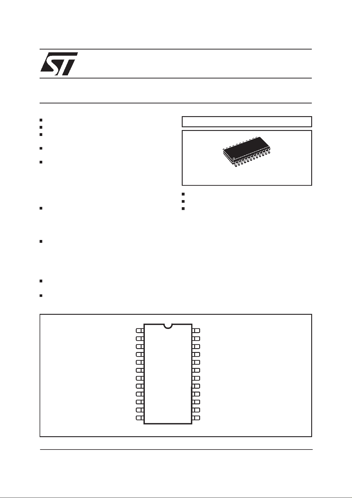
SO24
OPENGND
REVERSEDBATTERY
ESD
DESCRIPTION
The car radio diagnostic processor is an interface
chip in BCD Technology intended for car radio
applications. It is able to detect potential faults
comingfrom any misconnectionin thecar radio or
in the harnesswhen installingthe set.
The device is able to reveal any fault in the loudspeaker lines and in the antenna and booster
supply lines, providing a proper output signal (I
2
C
bus compatible) in order to disable the ICs under
fault and/or to alert µcontroller by means of warning messages.
PIN CONNECTION (Topview)
GND
SDA
SCL
ADD
W
AUX1 OUT
AUX1 IN
AUX2 IN
AUX2 OUT CH1-
5V CH1+
ST-BY T-CAP11 14
S
December 1999
This is preliminary information on a new product now in development or undergoingevaluation.Details are subject to change without notice.
2
3
4
5
6
7
8
9
10
D97AU570
24
23
22
21
20
19
18
17
16
15
1312V
CH5-1
CH5+
CH4+
CH4CH3CH3+
CH2+
CH2-
CURR. SET. RES.
1/15
Page 2
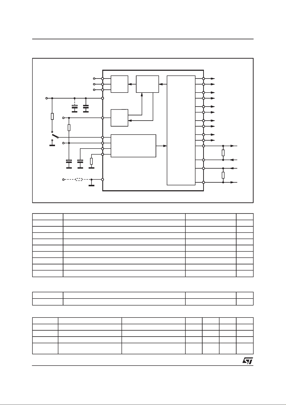
TDA7476
BLOCK DIAGRAM
SDA
SCL
ADD
V
S
C2
100nF
R
C
CS
T
R3
10KΩ
ST-BY
SW1
10KΩ
10∝F
DIG-GND
R4
C1
W
5V
REF
C3
10µF
R5 51Ω
ABSOLUTE MAXIMUM RATINGS
2
3
I2C INTERFACE
4
12
5
DELAY
CURRENT
FORCING
11
10
VOLTAGE
14
TEST SIGNAL GENERATOR
13
19
REGULATOR
&
&
COMPARATORS
24
23
22
21
20
19
18
17
16
15
6
7
8
RSENS1
RSENS2
D96AU499A
CH5
CH4
CH3
CH2
CH1
OUT
AUX1
IN
IN
AUX2
OUT
Symbol Parameter Value Unit
V
V
V
peak
P
T
stg;Tj
V
V
V
V
op
s
tot
SB
SDA
SCL
ADD
Operating Supply Voltage 18 V
DC Supply Voltage 28 V
Peak Supply Voltage t = 50ms 40 V
Total PowerDissipation Tcase = 25°C 1.5 W
Storage and Junction Temperature -40 to 150 °C
Stand-by Pin Voltage 6 V
SDA PinVoltage 6 V
SCL Pin Voltage 6 V
ADD Pin Voltage 6 V
THERMAL DATA
Symbol Parameter Value Unit
R
Th j-amb
ELECTRICALCHARACTERISTICS
Symbol Parameter Test Condition Min. Typ. Max. Unit
IN Stand-By IN Threshold 1.5 V
V
SB
OUT Stand-By OUT Threshold 3.5 V
V
SB
I
SB
Iq Total Quiescent Current Total quiescent Current with
Thermal resistance junction to ambient Max. 85 °C/W
= 14.4V;T
(V
s
=25°;RL=4Ω, unlessotherwise specified.)
amb
Stand-By Current Consumption Stand-By Voltage Pin = 1.5V 100 µA
5mA
TDA7476 not addressed
2/15
Page 3
TDA7476
ELECTRICALCHARACTERISTICS (continued)
Symbol Parameter Test Condition Min. Typ. Max. Unit
AUDIO INPUTS CH1, CH2, CH3, CH4,CH5 - TURN ON DIAGNOSTIC
Pgnd Short to GND det.(below this
limit, the Audio Output is
considerd in Short Circuit to
GND)
Pvs Short to Vsdet. (above this
limit, the Audio Output is
considered in Short Circuitto Vs)
Pnop Normal operation thresholds.
(Within these limits, the Audio
Output is considered without
faults)
Lsc Shorted Load det. (voltage
across the Audio Outputs).
Below this limit the load is
considered shorted.
Lop Open Load det. (voltage across
the Audio Outputs). Above this
limit the load is considered open.
Lnop Normal load det. (Voltage
across the Audio Output).
Within these limits the load
resistance is considered normal.
AUX INPUTS AUX1, AUX2 - TURN ON DIAGNOSTIC
Agnd Short to GND det.(voltage
across the sensing resistor).
Above this limit the AUX pin is
considered in Short Circuitto
GND.
Aol Open load det. (voltage across
the sensing resistor). Below this
limit the Aux pin is considered in
Open Load condition.
Anop Normal Operation det. (Voltage
across the sensing resistor).
Within these limits the load
resistance connected to the Aux
pin is considered correct.
AUDIO INPUTS - PERMANENT DIAGNOSTIC
Pgnd Short to GND det.(below this
limit, the Audio Output is
considered in Short Circuitto
Vs) This condition must be true
for a time higher than Tdel
Pvs Short to Vsdet. (above this limit
the Audio Output is considered
in Short Circuit to Vs) This
condition must be true for a time
higher than Tdel
Pnop Normal operation thresholds.
(Within these limits, the Audio
Output is considered without
faults)
Power amplifier in st-by
condition
High side driver ON 0.75 V
Power amplifier ON 0.8 V
Vs-0.7 V
1.2 Vs-1.3 V
550 mV
22 220 mV
0.125 0.5 V
Vs-0.7 V
1.2 Vs-1.3 V
0.8 V
5mV
0.085 V
3/15
Page 4
TDA7476
ELECTRICALCHARACTERISTICS (continued)
Symbol Parameter Test Condition Min. Typ. Max. Unit
AUX INPUTS - PERMANENT DIAGNOSTIC
Agnd Short to GND det.(above this
limit, the Audio Output is
considered in Short Circuitto
Vs) This condition must be true
for a time higher than Tdel
Aol Open load det. (voltage across
the sensing resistor. Below this
limit the Aux pin is considered in
Open Load condition)
This condition must be true for a
time higher than Tdel
Anop Normal Operation det. (Voltage
across the sensing resistor.
Within these limits the load
resistance connected to the Aux
pin is considered correct)
PERMANENT DIAGNOSTIC - ACQUISITION TIME DELAY
Tdel Acquisition time delay- The
fault is considered true if the
fault condition are present for
more than Tdel without
interruption
PERMANENT DIAGNOSTIC - WARNINGPIN
Vsat Saturation voltage on pin 5 Sink Current at Pin 5 = 1mA 1 V
ADDRESS SELECT
V
ADD
2
I
C BUS INTERFACE
f
SCL
V
IL
V
IH
V
SAT
Voltage on pin 4 Address 0100010X 1.5 V
Clock Frequency 400 KHz
Input Low Voltage 1.5 V
InputHigh Voltage 3 V
Sat Voltage at pin 2 Sink Current at Pin 2 = 5mA 1.5 V
WORKINGPRINCIPLES
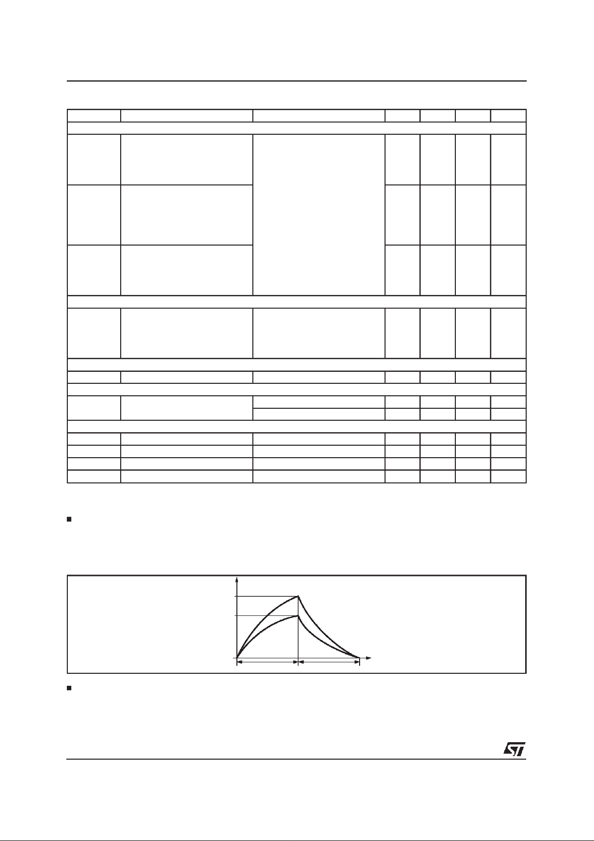
Turn-ondiagnostic - CH1, CH2, CH3,CH4, CH5 - Shorted load/openload detection
To detect a short across the load or an open load, a subsoniccurrent pulse is generated. The information related to the status of the outputs are measured and memorized at the top of the current
pulse (tm in fig.1). The current is sourced by the positive pins (CH1+,...CH5+) and it is sunk by the
correspondingnegativepins (CH1-,...CH5-).
Figure 1.
High side driver ON 0.75 V
0.085 V
0.125 0.5 V
2s
Address 0100011X 3 5 V
I(mA)
I
SOURCE
I
SINK
t
t
m
D97AU571
t
s
(ms)
Isink and Isource are dependingon the external resistor Rcs. The minimum allowed value for Rcs is
1.65KOhm.The relationshipamong Isink,Isource and Rcs is the following:
Isink = (3.3/Rcs)x 11
Isource= 1.5 x Isink
4/15
Page 5
TDA7476
On bridge (or bridgeequivalent) devices if thereis no short circuit to GND or to Vs, Isourcegoes into
saturation mode (for Vout > 3V), and in the load flows Isink. As the turn-on diagnosticthresholds are
fixed, it is possible to calculatethe ranges of loudspeakerresistance in which short circuit, normal operation and openload are detected.
For example, here below are two cases,with Rcs = 3.3KOhm and Rcs = 1.8KOhm. (R
= Vthr*/Isink).
L
Rcs = 3.3kΩ
Rcs = 1.8kΩ
S.C. across Load x Open Load
0Ω 2Ω 20Ω infinite
S.C. across Load x Open Load
0Ω 1.1Ω 11Ω infinite
0.5Ω 50Ω
0.27Ω 27Ω
xNormal Operation
xNormal Operation
D96AU500
The exact values of the above mentioned resistive ranges may vary a little, depending on the power
amplifier used. These valuesfor the variouspossible ST power amplifierswill be communicatedlater.
When single-ended devices are used and the application circuit is as shown in fig. 5,6,it is necessary
to use:
- a greater timing capacitor so that the time t
m
is high andthe outputs of the amplifiers are able to rise
over1V;
- a resistorR
CS 1.5 times higher than thatused for the bridge amplifiers.
In this case, the loudspeaker resistance ranges in which short circuit, normal operation and openload
are detectedwill be as followswith Rcs = 4.7KOhmand Rcs = 2.7KOhm(R
Rcs = 4.7kΩ
S.C. across Load x Open Load
0Ω 1.9Ω 19Ω infinite
0.47Ω 47Ω
xNormal Operation
= Vthr/Isource)
L
Rcs = 2.7k
S.C. across Load x Open Load
Ω
0Ω 1.1Ω 11Ω infinite
0.27Ω 27Ω
xNormal Operation
D96AU501
The exact values of the above mentioned resistive ranges may vary a little, depending on the power
amplifier used. These valueswill be communicatedlater.
Turn-ondiagnostic - CH1, CH2, CH3,CH4, CH5 - Short to GND and Vs.
To detect if there is short circuit to GND or Vs, the subsonic current pulse is exploited. The information
related to the status of the outputsare measured and memorized at the top of the current pulse (tm in
fig.1).If no faults are present,the pins connectedto the audio outputs (CH1,..CH5) will reach about 3V.
If one or more outputsare shorted to GND,these voltagesbecomelower than 3V.
If one or more outputsare shorted to Vs, the output voltageincreases over 3V.
The fault status can be know by sensing the output voltages. The reason way voltage threshold has
been preferred instead of a currentthreshold to declareshort circuit resistorranges is two fold:
1) The amplifier can draincurrent in the resistive path of the short circuit, hence this current and consequentlythe short circuit resistor cannot be determinedwith a sufficientlevel of accuracy.
2) The voltage differencebetweenthe car radio ground (reference)and the position of the chassis of the
car where the loudspeaker line is connected (due to an accidental short circuit) can be up to some
hundredsof mV. This doesnot permit a correctmeasure of the short circuit resistor.
(*) Vthr is the threshold described in the table on page 3/14 - 4/14 (for example Pgnd-min, Pvs - max, Pnop - min,Pnop - max etc..)
5/15
Page 6

TDA7476
Turn-ondiagnostic - AUX1, AUX2
To detect if thereis a short circuitto GND or an open load involvingto the AUX output of the car radio,
the voltage acrossa sensing resistorRsens is detected.
These output voltages (for example for the active antenna and for the booster) are usually generated
by highside drivers,but also voltage regulatorswith Vout > 5V areadmissible.
The detectionrangescan be set by adjustingthe sensingresistors Rsens1or Rsens2.
For example, if Rsens = 5Ohm,the following detection table will be operative(I = Vthr/Rsens):
Open LoadxS.C. to GND
xNormal Operation
100mA 25mA
150mA 17mA
Permanentdiagnostic - CH1, CH2, CH3,CH4, CH5 - Short to GND and Vs
During the CAR-RADIO normal operation, to detect a short circuit to GND (or to Vs), the output voltages are sensed. If one or more outputs stay at any voltagebelow0.8V or over Vs-0.8V for morethan
2 sec.(typ), the warning pin is pulled down.
TheµP can addressthe TDA7476to knowthe status.
The subsonic current pulse is activated also in this case. The fault is correctly detected if it remains
until thememorization (tm in fig.1).
In this phase,faults regardingshorts across the loadand open loadscannot be detected.
For single-ended devices as in fig. 5, 6 a short citcuit to ground is detected both when a short to
ground is really presentand when the load is missing.
D96AU503
Permanentdiagnostic - AUX1, AUX2 - Shortcircuit to GND and open load
The detection mode of the auxiliary inputs is equal to what is in place during turn-on, but the fault
must be lastingwithout interruption for more than2 seconds.
The warningpin is pulleddown only in case of shortto GND. This is toavoid that this pin remains permanently to 0 level if one or both AUXoutputsof the car radioare unused.
Timing
From the byte ”ADD1” to the byte ”ADD2” the µP must wait a period Twait1(see Software Specification) that is depending on the timingcapacitor C
CT(µF) t
3.3 45
4.7 65
10 130
22 290
47 620
100 1300
T
accordingto thefollowingtable (Twait1> tm, max):
(ms)
m max
Note: any (positive) spread of the capacitor value must be added. The relation to be used to determine
Twait1 from the value of C
T accordingto the following:
Twait1> tm, max= (130 x C
T/10µF)ms
After the byte ”ADD2” the poweramplifier can be switched-on.In some cases,the µP has to wait until
the current pulse is finished (Twait2). This time(ts in fig.1) is givenby:
Twait2 > ts, max = (140 x C
T
/10µF)ms
For bridge or bridge equivalent devices (figg.7,8), Cs = 10µF willbe enough.
For the TDA7375,connected as in fig.5, Cs = 47µF if Cout = 1000µF, andCs = 100µF if Cout= 2200µF.
If the circuit is as shown by fig. 6, the suggested values of Cs are as follows: Cs = 22µF if Cout =
1000µF, Cs = 47µF ifCout = 2200µF.
6/15
Page 7

TURN-ON DIAGNOSTIC - THRESHOLDS
CH1, CH2,CH3, CH4, CH5
Outputvoltage during test. (The power amplifiermust be in ST-BYmode).
S.C. to GND x S.C. to Vs
xNormal Operation
TDA7476
0V 1.2V V
0.8V V
-1.3 V
S
-0.7V
S
D96AU502A
S
Voltageacross the load during test. (The power amplifier must be in ST-BYmode).
S.C. acrossLoad x Open Load
0V 22mV 220mV V
5mV 550mV
xNormal Operation
D97AU631A
S
Note: some faults can mask others if they are presentat the same momenton the same channel:
- If there is a short to GND and an open load on the same channel, the TDA7476gives information
only aboutone of them, dependingon the wire on which the short circuit is present.
- Theshort circuit to GND masks any short circuit acrossthe load.
- Theshort circuit to Vs masks anyshortor open load.
AUX1 - AUX2
Voltageacross the sensing resistors.
S.C. to GND x Open Load
V
S
0.5V 125mV 0V
0.75V 85mV
xNormal Operation
D97AU572
The minimum voltage of the AUX IN pin to sense the open load conditionis 2V.
The minimum voltage of the AUX IN pin to detectthe short circuit to GND, by sensing the drop on the
resistors is 4.5V. If this voltage falls below 2V, the AUX in is consideredshort circuited to GND. From
2V to 4.5Vthe sensingcircuit can detect a shortcircuit in bothways (by sensing across the resistor or
throughthe voltagebetweenthe AUX INpin andGND).
PERMANENTDIAGNOSTIC - THRESHOLDS
CH1, CH2,CH3, CH4, CH5
The circuit will recognize as a fault condition any situation where the following short circuit voltages
last morethan 2 sec (typ).
Outputvoltage
S.C. to GND x S.C. to Vs
0V 1.2V V
0.8V V
xNormal Operation
-1.3 V
S
-0.7V
S
D97AU573A
S
AUX1 - AUX2
The voltage across the resistorsRsens1 or Rsens2 is sensed. The circuit will recognizeas a faultcondition any situation where the following voltages last more than 2sec (typ) in the region ”S.C.to GND”
or ”openload”.
S.C. to GND x Open Load
V
S
0.5V 125mV 0V
0.75V 85mV
xNormal Operation
D97AU574
The minimum voltage of the AUX IN pins to sense the open load conditionis 2V.
The minimum voltage of the AUX IN pin to detect the short circuit to GND by sensing drop on the re-
sistor is 4.5V. If thisvoltage is below 2V, the AUX line is consideredshort circuited to GND. From 2V
to 4.5V the sensing circuit can detect a short circuit in both ways (by sensing across the resistor or
throughthe voltagebetweenthe AUX INpin andGND).
7/15
Page 8

TDA7476
I2C BUS INTERFACE
Data transmission from microprocessor to the
TDA7476 and viceversa takes place through the
2 wires I
2
C BUS interface, consisting of the two
lines SDA and SCL (pull-up resistors to positive
supply voltage mustbe connected).
Data Validity
As shown by fig. 2, the data on the SDA line must
be stable during the high period of the clock. The
HIGH and LOW state of the data line can only
change when the clock signal on the SCL line is
LOW.
Start and Stop Conditions
As shown by fig. 3 a start condition is a HIGH to
LOW transition of the SDA line while SCL is
HIGH. The stop condition is a LOW to HIGH transition of the SDA line while SCL is HIGH.
Figure 2:
Data Validityon theI
2
CBUS
Byte Format
Every byte transferred to the SDA line must contain 8 bits. Each byte must be followed by an acknowledgebit. The MSB is transferredfirst.
Acknowledge
The transmitter* puts a resistive HIGH level on the
SDA line during the acknowledge clock pulse (see
fig.4).The receiver**the acknowledgeshasto pulldown (LOW) the SDA line duringthe acknowledge
clock pulse, so that the SDAlineis stableLOW duringthis clockpulse.
* Transmitter
= master (µP) when it writes an address to
the TDA7476
= slave (TDA7476) when the µP reads a
data byte fromTDA7476
** Receiver
= slave (TDA7476) when the µP writes an
addressto the TDA7476
= master (µP) when it reads a databyte from
TDA7476
Figure 3: TimingDiagram on the I
Figure 4:
8/15
Acknowledgeon theI
2
2
CBUS
CBUS
Page 9

TDA7476
SOFTWARESPECIFICATIONS
The TDA7476 is activated by turning-on the ST-BY pin (CMOS compatible). In this condition it waits for
2
theI
CBusaddressingbyte ADD1 (WRITE to TDA7476)
ADD1
S 010001A 0 ACK P
This sequence(where the bit 0 of ADD1 isat 0 level) enables the acquisition routine andstarts the single
pulse (containing infrasonic harmonics) for the test. During this period the data regarding all the outputs
are memorized.
After a period Twait1that depends on thevalue of the timing capacitor (see Timing)the µP redirects the
TDA7476by the byte ADD2.
ADD2
S 010001A 1 ACK BYTE 1 ACK BYTE 2 ACK BYTE3 ACK STOP
The byte ADD2 contains the bit 0 at 1 level. This enables the reading mode, TDA7476’s. The 3 bytes
with the diagnosticinformation BYTE1, BYTE2, BYTE3 (READ FROM TDA7476) are nowtransmitted to
theµP.
The addressof TDA7476 is selected using pin ADD (pin 4) .
If ADD is connected to ground,then A = 0 and the TDA7476addressis 0100010X.
If ADD is connected to 5V,than A = 1 and the TDA7476 address is 0100011X
The TDA7476 provides two types of diagnosticinformation:
A) TURN-ON DIAGNOSTIC - The first time that the TDA7476 is addressed by I
plete set of diagnosticinformation is activated:
- CH1,CH2, CH3, CH4, CH5
ShortCircuit to GND
ShortCircuit to Vs
OpenLoad (*)
ShortCircuit across the load (*)
(*)Detectedif the power amplifiers are in ST-BYcondition.
- AUX1,AUX2
ShortCircuit to GND (*)
OpenLoad (*)
(*)Detectedif the high side driversattached to the Aux outputsare ON.
Here followingthe turn-ondiagnosticoutput bytes
2
CBus, the more com-
9/15
Page 10

TDA7476
READ BYTE 1
MSB LSB
D7 D6 D5 D4 D3 D2 D1 D0
XXXX11X0CH1short circuitto Vs
XXXX110XCH1short circuitto GND
XXXX1011CH1open load
XXXX0111CH1short circuitacross the load
1 1 X 0 X X X X CH2 short circuitto Vs
1 1 0 X X X X X CH2 short circuit to GND
1 0 1 1 X X X X CH2 open load
0 1 1 1 X X X X CH2 short circuit across the load
READ BYTE 2
XXXX11X0CH3short circuitto Vs
XXXX110XCH3short circuitto GND
XXXX1011CH3open load
XXXX0111CH3short circuitacross the load
1 1 X 0 X X X X CH4 short circuitto Vs
1 1 0 X X X X X CH4 short circuit to GND
1 0 1 1 X X X X CH4 open load
0 1 1 1 X X X X CH4 short circuit across the load
READ BYTE 3
X X X X X X 1 0 AUX1 short circuit to GND
X X X X X X 0 1 AUX1 open load
XXXX10XXAUX2 short circuit to GND
XXXX01XXAUX2 open load
1 1 X 0 X X X X CH5 short circuitto Vs
1 1 0 X X X X X CH5 short circuit to GND
1 0 1 1 X X X X CH5 open load
0 1 1 1 X X X X CH5 short circuit across the load
STATUS
When the µP reads correctly all the 3 bytes containing the mentionedinformation and gives the last acknowledge, the TDA7476 switches to the ”permanent diagnosticoperation”
PERMANENT DIAGNOSTIC
B)
It can sensethe followingdiagnosticinformation:
CH1, CH2, CH3, CH4, CH5
- ShortCircuit toGND
- ShortCircuit toVs
Aux1, Aux2
- ShortCircuit toGND (*)
- OpenLoad (*)
(*) Detected if the high side driversattached to the Auxoutputs are ON.
In this case the above conditionsare not detected while the single infrasonic current pulse is present
but before. The fault conditionmust be present for more than 2sec. (typ) and must be also true during the pulse,where the data are memorizedand then transmitted.
The bytes from/to µPand TDA7476 are the same asthose in case of turn-on diagnostic (see above).
Here following is the permanent diagnostic output Data Bytes. The bits D7 and D6 of the first byte both
stand at 0 level. This condition,although not possibleduring the turn-on diagnostic, can be usefulto confirm that the bytes are referredto the permanentdiagnostic.
10/15
Page 11

TDA7476
READ BYTE 1
MSB LSB
D7 D6 D5 D4 D3 D2 D1 D0
0 0 X X 1 1 X 0 CH1 short circuit to Vs
0 0 X X 1 1 0 X CH1 short circuit to GND
00XX1111
00XX1111
0 0 X 0 1 1 X X CH2 short circuit to Vs
0 0 0 X 1 1 X X CH2 short circuit to GND
001111XX
001111XX
READ BYTE 2
1 1 X X 1 1 X 0 CH3 short circuit to Vs
1 1 X X 1 1 0 X CH3 short circuit to GND
11XX1111
11XX1111
1 1 X 0 1 1 X X CH4 short circuit to Vs
1 1 0 X 1 1 X X CH4 short circuit to GND
111111XX
111111XX
READ BYTE 3
1 1 X X X X 1 0 AUX1 short circuitto GND
1 1 X X X X 0 1 AUX1 open load
1 1 X X 1 0 X X AUX2 short circuit to GND
1 1 X X 0 1 X X AUX2 open load
1 1 X 0 X X X X CH5 short circuitto Vs
1 1 0 X X X X X CH5 short circuit to GND
1111XXXX
1111XXXX
Repetitiveturn-on diagnostic
During the turn-ondiagnostic,the TDA7476can revealfalse ”shortcircuit acrossload”and/or false ”open
load” dueto noise sources such as door slams.
This problem can be solved doing more than one turn-on diagnostic routine. If the µP asks for N times
the state of the audio system, it has to consider a fault as really present only if it is detected in all the N
turn-on diagnostic.
As above explained, the first time the TDA7476 receivers the byte ADD1, it does the turn-on diagnostic;
then each timeit is addessed with ADD1, it does the permanent diagnostic. This is not true if, when the
µP sendsfor the forsttime the byte ADD2, it doesnot send to the TDA7476 the acknowledgeafter it has
received the byteBYTE3.In this case, the TDA7476does not switch from turn-on to permanentdiagnostic mode so if it receivesagain the byte ADD1 it works as it was the first time that it doesthe turn-on diagnostic.In orderto do repetitiveturn-on diagnostic,the µP has to be programmed as following:
Step 1: the µP sends ADD1
STATUS
START ADD1 ACK STOP
Step 2: the µP waits Twait1seconds
Step 3: the µP sends ADD2, receivesBYTE1, BYTE2, BYTE3,
does not send the acknowlegdeaf-
ter BYTE3
START ADD2 ACK BYTE1 ACK BYTE2 ACK BYTE3 STOP
Step 4: repeat Step1, Step2, Step3 while the second, third, fourth, ...turn-on diagnostic has to be
done.
During the last turn-on diagnostic the µP sends ADD2, receives BYTE1, BYTE2, BYTE3, and
sends the acknowlegdeafter BYTE3
START ADD2 ACK BYTE1 ACK BYTE2 ACK BYTE3 ACK STOP
11/15
Page 12

TDA7476
In this way only after that the TDA7476 has done for N times the turn-on diagnostic, it switches from
turn-on to permanentdiagnosticmode.
From now the TDA7476 always does the permanentdiagnostic.
To save time when the audio system is switched on, it is possible to do the repetitive turn-on diagnostic
when the car-radio is turned off. In this case the steps to follow to do the repetitiveturn-on diagnosticare
the following:
1- to switch off the TDA7476 connectingSTBY pin to ground;
2- towaitT
3- to switch on the TDA7476
4- to do the repetitive turn-on diagnosticas above described;
5- to turn off the TDA7476.
WARNING PIN
This is an open drain output pin that is activated when a fault condition is present for more than 2 sec
(TYP). The fault conditionsrelated to the warningpin areas follows:
- AUX1,AUX2
- CH1, CH2, CH3,CH4, CH5:
The purposeof this pin is to alert the µP and start with the permanentdiagnostic routine only if faults
are present,thus avoidingCPU’s wasteof time.
5V seconds(timenecessaryforthe dischargeofthe capacitor).If C5V =10µFthenT5V =20mstyp;
Shortto GND
ShortCircuit to GND
ShortCircuit to Vs
APPLICATIONNOTES
On single-ended devices as in figure 6, 7 if the loads are present then both in turn-on and in permanent diagnosticthe fault present on one channelis pointed out forall the loads connected together.
For example:
- seefig.6if CH1+isshortedtoground,theTDA7476revealsa shortto groundboth forCH2andforCH1.
- seefig.7ifCH1+isshorte dto groun d,theTDA 7476detectsa shortcircuittogroundforCH1,CH2,CH3, CH4.
To use the TDA7476 with a car-radio system which has less than five audio channel and less than
two auxiliary loads, it isnecessaryto takesome cares:
- If the loadsare 4Ω speakers(Rcs= 3.3 KΩ),R ≅ 10Ω has to be connectedbetween CH+ and CH- of
eachchannel(see figg. 5,6,7,8 concerning CH5). R ≅ 5Ω has to be used if loadsare 2Ω speakers
(Rcs=1.8 KΩ).
- If AUX1/AUX2are unused, Rsens1/Rsens2will not be needed.The AUX-INpin(s)can be tied to the
5 internalregulator(pin 10) while setting the AUX-OUT pin(s) about 250mV lower thanAUX-IN’s
(admissiblerange= 125mVto 500mV). This can easilybe obtainedby means of a voltage divider.
IfboththeAUXchannelsare unused,pins7-8 (AUX-IN s )andpins6-9(AUX-OUT s)canbe respectively
connectedtogether, so thata single voltage divider couldbe used.
The above actions will prevent any ”warning” activation which might cause unwanted microprocessor’s
interrupt.
12/15
Page 13

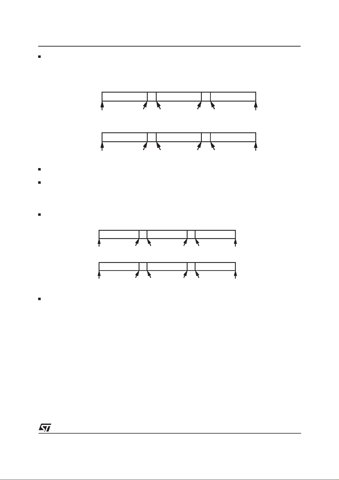
APPLICATIONEXAMPLES WITHST AUDIO POWER ICs
Figure 5: TDA7375in S.E. mode with 4 output capacitors
TDA7476
Figure 6:
TDA7375
+-
-+
+-
-+
CH1+ CH2+ CH3+ CH4+ CH5+RCH5- CH4- CH3- CH2- CH1-
D97AU575A
TDA7476
TDA7375in S.E. mode with 2 outputcapacitors
TDA7375
+-
-+
+-
-+
CH1+ CH2+ CH3+ CH4+ CH5+ CH5- CH4- CH3- CH2- CH1-
D97AU576A
R
TDA7476
C
OUT1
C
OUT2
C
OUT3
C
OUT4
C
OUT1
C
OUT2
Figure 7:
TDA7451
D97AU577A
Figure 8: QuadBridge Amplifiers
D97AU578A
TDA7451
+-
-+
+-
-+
R
CH1+ CH2+ CH3+ CH4+ CH5+ CH5- CH4- CH3- CH2- CH1-
TDA7476
TDA7384, TDA7385, TDA7386, TDA7454
+-
-+
+-
-+
R
CH1+ CH2+ CH3+ CH4+ CH5+ CH5- CH4- CH3- CH2- CH1-
TDA7476
13/15
Page 14

TDA7476
DIM.
MIN. TYP. MAX. MIN. TYP. MAX.
A 2.35 2.65 0.093 0.104
A1 0.10 0.30 0.004 0.012
A2 2.55 0.100
B 0.33 0.51 0.013 0.0200
C 0.23 0.32 0.009 0.013
D 15.20 15.60 0.598 0.614
E 7.40 7.60 0.291 0.299
e 1.27 0,050
H 10.0 10.65 0.394 0.419
h 0.25 0.75 0.010 0.030
k0°(min.), 8° (max.)
L 0.40 1.27 0.016 0.050
mm inch
OUTLINEAND
MECHANICAL DATA
SO24
0.10mm
.004
Seating Plane
1
A2
A
Be
A1
K
D
1324
E
12
hx45°
L
A1 C
H
SO24
14/15
Page 15

TDA7476
Information furnished is believed to be accurate and reliable. However, STMicroelectronics assumes no responsibility for the consequences
of use of such information nor for any infringement of patents or other rights of third parties which may result from its use. No license is
granted by implication or otherwise under any patent or patent rights of STMicroelectronics. Specification mentioned in this publication are
subject to change without notice. This publication supersedes and replaces all information previously supplied. STMicroelectronics products
are not authorized for use as critical components in life support devices or systems without express written approval of STMicroelectronics.
Australia - Brazil - China - Finland- France - Germany - Hong Kong - India - Italy - Japan - Malaysia - Malta - Morocco -
The ST logo is a registered trademark of STMicroelectronics
1999STMicroelectronics – Printedin Italy – AllRights Reserved
STMicroelectronics GROUP OF COMPANIES
Singapore - Spain - Sweden - Switzerland - United Kingdom - U.S.A.
http://www.st.com
15/15
 Loading...