

Page 1
QUAD BTL DRIVER WITH VOLTAGE REGULATOR
4 BUILT-INPOWERBRIDGES(4 x 0.6A)
NO EXTERNAL COMPONENTS
SINGLEPOWERSUPPLY
WIDESUPPLY VOLTAGE RANGE (6 TO15V)
5V REGULATOR DRIVER FOR EXTERNAL
PASS TRANSISTOR WITH FOLD-BACK
SHORTCIRCUIT PROTECTION
ADJUSTABLE REGULATOR (2.0 TO 3.6V @
200mA) WITH SHORT CIRCUIT PROTECTION
TDA7473
SO28 (24+2+2)
DESCRIPTION
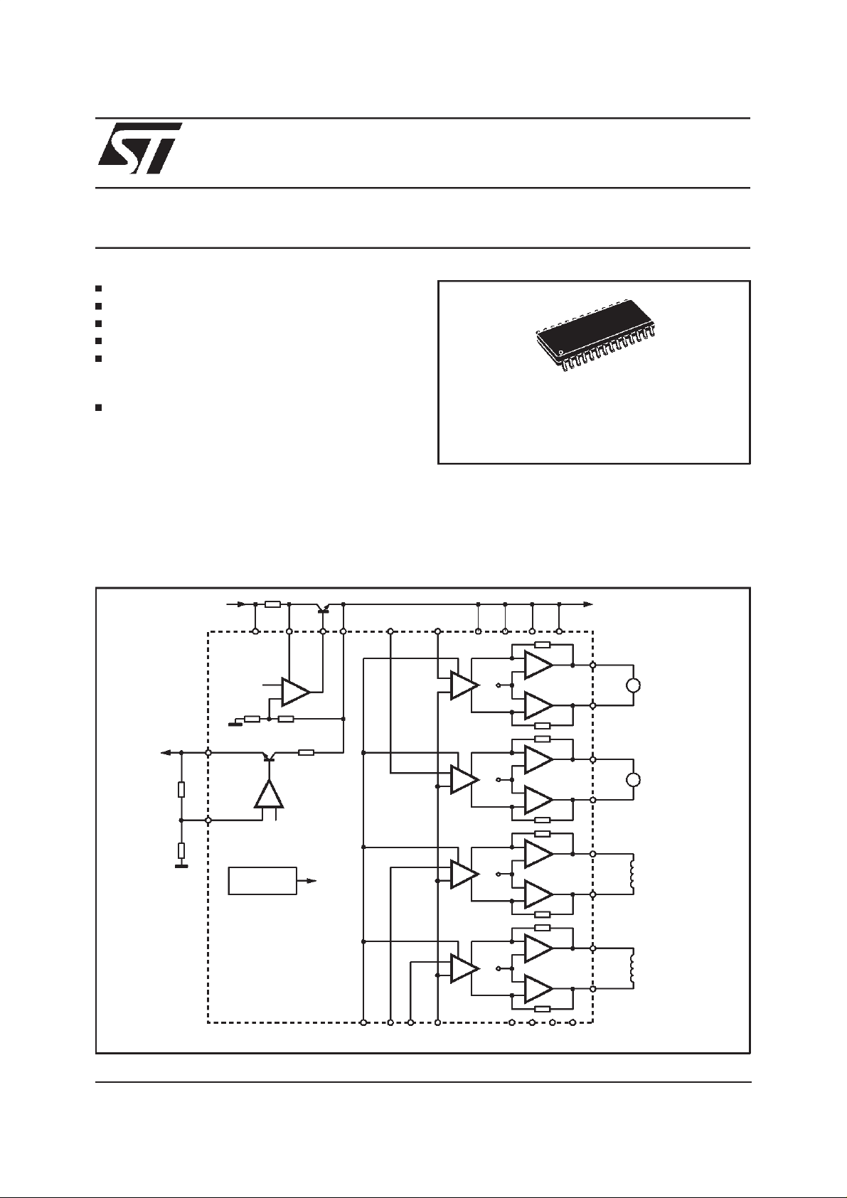
This device is a quad power driver circuit in BTL
configuration, intended for use as a power driver
for servo systems with a singlesupply.
It’s specially dedicated to compact disc players
and it’s capable of driving focus & tracking actuators sledge & spindle motors.
The regulators are mainly used to have a 5V supply for the power part and a lower programmable
voltagefor the logic circuits.
Figure 1: Quad BTL PowerBridges + MultifunctionRegulators.
+
R1
1K
R2
1K
REG
ADJ
VSUP
VBG
REFERENCE
OC
VBG
VBG
5V
VS1 VS2
+
-
+
-
+
-
VS/2
VS/2
VS/2
VS3IN2 IN1DRIV
VS4
-
+
+
-
-
+
+
-
-
+
+
-
OUT 1+
OUT 1-
OUT 2+
OUT 2-
OUT 3+
OUT 3-
SPINDLE
M
MOTOR
SLEDGE
M
MOTOR
TRACKING
ACTUATOR
June 1998
IN3
ST_BY IN4
COMM
REF
-
+
VS/2
+
-
+
-
GND GND GND GND
OUT 4+
OUT 4-
D95AU223B
FOCUS
ACTUATOR
1/5
Page 2

TDA7473
PIN CONNECTION (Topview)
5V
VSUP
OUT1-
VS1
OUT1+
GND
GND
ADJ
OUT2+ OUT3+
VS2
OUT2- OUT3-
ST_BY
REG
2
3
4
5
6
7
8
9
10
11
12
13
D95AU310A
28
27
26
25
24
23
22
21
20
19
18
17
16
1514
PIN FUNCTIONS
N. Pin Name Description
1 5V 5V regulated input
2 VSUP Positive power supply(battery)
3 OUT1- 1.st channel negative output
4 VS1 1.st channel power supply
5 OUT1+ 1.st channel positive output
6 OC Overcurrent sense input
7 GND Ground
8 GND Ground
9 ADJ Regulated voltage adjust input
10 OUT2+ 2.nd channel positive output
11 VS2 2.nd channel powersupply
12 OUT2_ 2.nd channel negativeoutput
13 ST_BY Stand_by
14 REG Regulated voltage output
15 COMM Common negative input
16 IN2 Positive input for the 2.nd channel
17 OUT3- 3.rd channel negative output
18 VS3 3.rd channel power supply
19 OUT3+ 3.rd channel positive output
20 IN3 Positive input for the 3.rd channel
21 GND Ground
22 GND Ground
23 IN4 Positive input for the 4.th channel
24 OUT4+ 4.th channel positive output
25 VS4 4.th channel power supply
26 OUT4- 4.th channel negative output
27 IN1 Positive input for the 1.st channel
28 DRIV Pass transistor driver
DRIV1
IN1
OUT4VS4
OUT4+
IN4OC
GND
GND
IN3
VS3
IN2
COMM
2/5
Page 3

ABSOLUTE MAXIMUM RATINGS
Symbol Parameter Value Unit
V
SUP
V
S
T
OP
T
J
DC Supply Voltage 18 V
Channel Power Supply 6 V
Operating TemperatureRange -25 to 80 °C
Maximum Junction Temperature 150 °C
THERMAL DATA
Symbol Parameter Value Unit
R
th j-amb
R
th j-pins
(*) with 6cm2of copper heatsink on board.
Thermal Resistance Junction to Ambient Max. 50 (*) °C/W
Thermal Resistance Junction to Pins Typ. 17 °C/W
TDA7473
ELECTRICALCHARACTERISTICS (@ V
SUP
= 6V, T
=25°C,unless otherwise specified.)
amb
Symbol Parameter Test Condition Min. Typ. Max. Unit
V
SUP
Supply Voltage 6 15 V
Maximum Power Dissipation (1) 1.5 W
Quiescent current (2) from V
S
Quiescent current (2) from 5V V
Quiescent current (2) from V
SUPVSUP
Stand-by current from 5V (pin1) V
Stand-by current from V
SUP
V
(pin4, 11,18, 25)
(pin1) = 5V, R2 = ∞ 1.8 2.5 mA
= 15V 1.3 2.5 mA
=6V 1 2 mA
V
SUP
= 5V, R2 =
(pin1)
V
= 15V 0.4 0.8 mA
SUP
= 6V 0.3 0.6 mA
V
SUP
=5V 20 35 mA
∞
1.2 2 mA
CHANNELS BTL
Peakoutput current for channels 0.6 A
V
SAT
VSATHIGH SIDE I = 0.6A;VS= 5V 1.3 1.6 A
VSATLOW SIDE I = 0.6A;V
Output voltageswingpeak-to-
V
= 5V, I
S
= 5V 0.7 0.9 A
S
= 0.6A 5.5 6 Vpp
out
peak
Voltage gain for channels 25.5 26.5 27.5 dB
Channels output offset voltage -180 -50 100 mV
VST-BY Channel St-By Threshold Active --> St-By 0.65V
St-By --> Active 0.50V
reg
0.75V
reg
reg
0.85V
reg
REGULATORS
5V Vpin 1 Iout = 0.2A 4.85 5.05 5.25 V
V
= 0.2A 1.2 1.3 V
out
50 100 mA
I
DRIV
Mindrop 5V -->REG I
Output currentfrom DRIV for
pass-transistor driving
Output current from DRIV in
20 50 80 mA
stand-by
DROP V
--> DRIV I
SUP
Threshold voltage for overcurr.
protection (VSUP - OC)
V
REG
Regulator Voltage R1, R2 = 1K
= 20mA 0.2 0.25 V
DRIV
= 6V 190 230 270 mV
V
SUP
= 12V 120 160 200 mV
V
SUP
= 15V 80 100 120 mV
V
SUP
Ω
2.45 2.53 2.65 V
Min REG voltage (settable) 1.8 2 V
Max REG voltage (settable) 3.6 3.8 V
Output current from REG in
R1, R2 = 1K
Ω
20 mA
Stand-by
(1) @ T
(2) INx = COMM; no loads on the regulatorsoutputs
(3) Device is active when St-By = Low
=70°C, on board 6cm2copper heatsink
amb
V
V
3/5
Page 4

TDA7473
SO28 PACKAGEMECHANICAL DATA
DIM.
MIN. TYP. MAX. MIN. TYP. MAX.
A 2.65 0.104
a1 0.1 0.3 0.004 0.012
b 0.35 0.49 0.014 0.019
b1 0.23 0.32 0.009 0.013
C 0.5 0.020
c1 45°(typ.)
D 17.7 18.1 0.697 0.713
E 10 10.65 0.394 0.419
e 1.27 0.050
e3 16.51 0.65
F 7.4 7.6 0.291 0.299
L 0.4 1.27 0.016 0.050
mm inch
S8
(max.)
°
4/5
Page 5

TDA7473
Information furnished is believed to be accurate and reliable. However, STMicroelectronics assumes no responsibility for the consequences
of use of such information nor for any infringement of patents or other rights of third parties which may result from its use. No license is
granted by implication or otherwise under any patent or patent rights of STMicroelectronics. Specification mentioned in this publication are
subject to change without notice. This publication supersedes and replaces all information previously supplied. STMicroelectronics products
are not authorized for use as critical components in life support devices or systems without express written approval of STMicroelectronics.
The ST logo is a registered trademark of STMicroelectronics
1998 STMicroelectronics – Printed in Italy– All Rights Reserved
STMicroelectronics GROUP OF COMPANIES
Australia - Brazil-Canada - China - France - Germany - Italy - Japan - Korea - Malaysia - Malta- Mexico - Morocco - The Netherlands -
Singapore - Spain - Sweden - Switzerland - Taiwan - Thailand - United Kingdom - U.S.A.
5/5
 Loading...