

Page 1
CAR RADIO SIGNAL PROCESSOR
DEVICE INCLUDES AUDIO PROCESSOR,
STEREO DECODER, NOISEBLANKER AND
MULTIPATHDETECTOR
HIGH PERFORMANCE SIGNAL PROCESSOR
NO EXTERNALCOMPONENTSREQUIRED
FULLY PROGRAMMABLEVIAI
LOW DISTORTION
LOW NOISE
2
C BUS
TDA7460N
SO20
DESCRIPTION
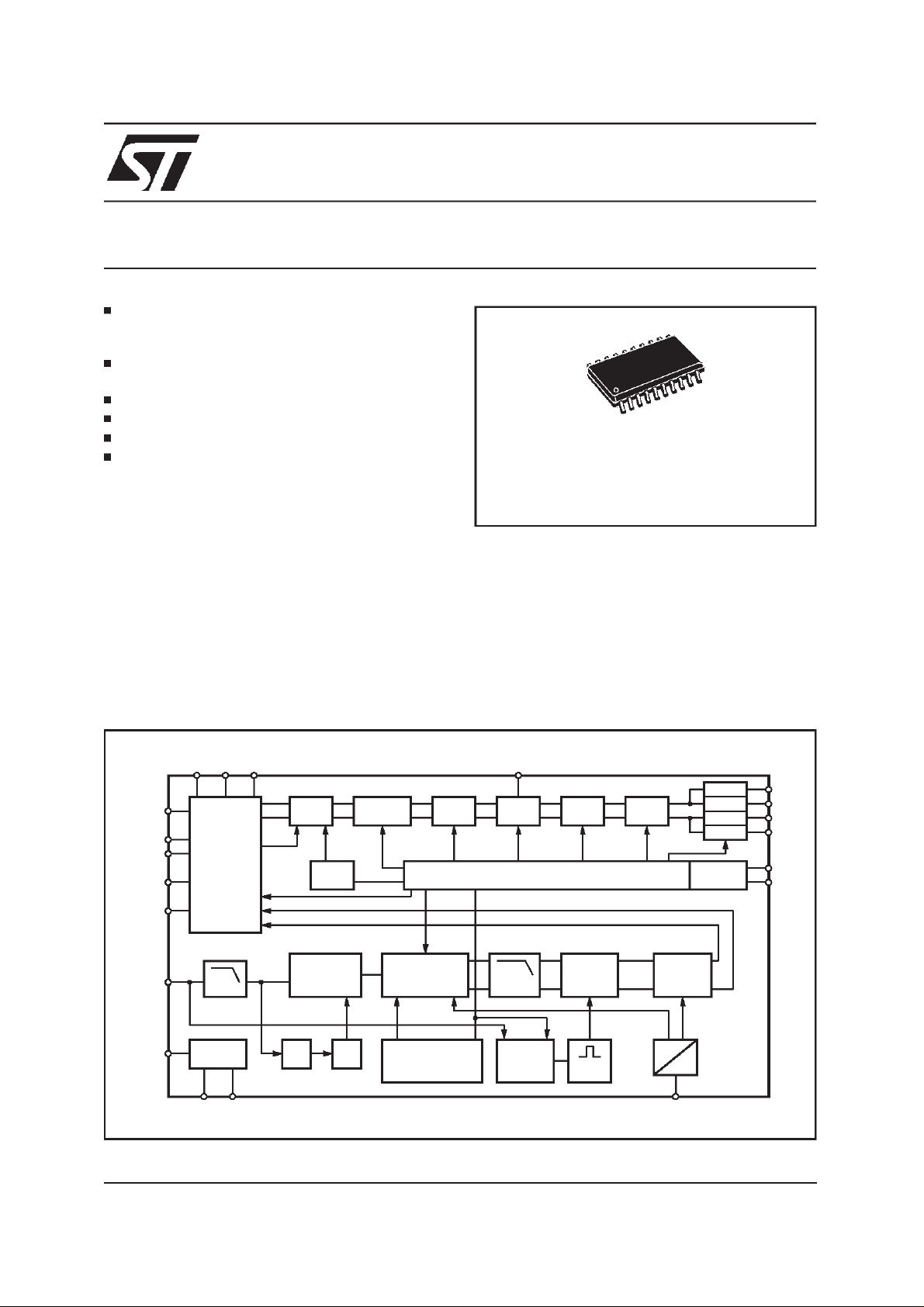
The TDA7460N is a high performance signal
processor specifically designed for car radio applications.
The device includes a complete audioprocessor
and a stereo decoder with noiseblanker,
stereoblend and all signal processing functions
necessary for state-of-the-artas well as future car
radio systems.
Switched-capacitors design technique allows to
obtain all these features without external compo-
BLOCK DIAGRAM
PHONE
(MPOUT)
CASS R
CASS L
PHONE
(MPIN)
GND
AM
CDL CDG CDR
8
1
INPUT
2
MULTIPLEXER
7
AUTO ZERO
6
345 11 17
MIXING
STAGE
PHONE
+
FM R
FM L
LOUDNESS
BEEP
ORDERING NUMBER: TDA7460ND
nents or adjustments. This means that higher
quality and reliability walks alongside an overall
cost saving.
The CSP is fully programmable by I
face allowingto customize key device parameters
and especiallyfilter characteristics.
The BICMOS process combined with the optimized signal processing assure low noise and
low distortionperformances.
SMUTE
OUT LR
VOLUME BASSTREBLE
SOFT
MUTE
DIGITAL CONTROL
OUT LF
OUT RR
OUT RF
2
C BUS
I
2
C bus inter-
OUT LR
19
OUT LF
16
OUT RR
18
OUT RF
12
SCL
13
SDA
MPX
V
June 2000
9
80KHz
LP
15
SUPPLY
S
14 20
CREF
GND
PILOT
CANCELLATION
PLL
PIL
DET
DEMODULATOR
+ STEREO
ADJUST
+ STEREO BLEND
MULTIPATH-
DETECTOR
25KHz
LP
NOISE
BLANKER
S&H
PULSE
FORMER
HIGH
CUT
CONTROL
D
A
10
LEVEL
D97AU629A
1/31
Page 2

TDA7460N
ABSOLUTE MAXIMUM RATINGS
Symbol Parameter Value Unit
V
S
amb Operating Ambient Temperature Range -40 to 85 °C
T
stg Storage Temperature Range -55 to 150 °C
T
SUPPLY
Symbol Parameter Test Condition Min. Typ. Max. Unit
S Supply Voltage 7.5 9 10 V
V
S Supply Current V
I
SVRR Ripple Rejection @ 1KHz Audioprocessor (all filters flat) 60 dB
ESD
All pins are protected against ESD according to the MIL883standard.
PIN CONNECTION
Operating Supply Voltage 10.5 V
=9V 253035mA
S
Stereodecoder + Audioprocessor 45 dB
CASS R
CASS L
CDR
CDGND
CDL
PHGND (MPOUT)
PHONE (MPIN)
AM
MPX SCL
LEVEL SMUTE
2
3
4
5
6
7
8
9
10
20
19
18
17
16
15
14
13
12
11
D97AU628A
CREF1
OUT LF
OUT RF
OUT LR
OUT RR
V
S
GND
SDA
THERMAL DATA
Symbol Parameter Value Unit
R
th-j pins
Thermal Resistance Junction-pins Max 85 °C/W
2/31
Page 3

TDA7460N
PIN DESCRIPTION
N. Name Function Type
1 CASSR Cassette Input Right I
2 CASSL Cassette Input Left I
3 CDR CD Right ChannelInput I
4 CDGND Ground reference CD I
5 CDL CD Left ChannelInput I
6 PHGND Phone Ground (MPOUT selectable by SW
7 PHONE Phone Input (MPIN selectable by SW
8 AM AM Input I
9 MPX FM Input (MPX) I
10 LEVEL Level Input Stereodecoder I
11 SMUTE Soft Mute Drive I
12 SCL I
13 SDA I
2
C Clock Line I/O
2
C Data Line I/O
14 GND Supply Ground S
15 VS Supply Voltage S
16 OUTRR Right Rear Speaker Output O
17 OUTLR Left Rear Speaker Output O
18 OUTRF Right Front Spaeaker Output O
19 OUTLF Left Front Speaker Output O
20 CREF Reference Capacitor Pin S
1
)I
1
)I
(1) See input configuration tree and databyte specification ”configuration”
Pin type legenda:
I = Input
O = Output
I/O = Input/Output
S = Supply
3/31
Page 4

TDA7460N
AUDIO PROCESSORPART
Input Multiplexer
Fully differential or quasi-differential CD and
cassettestereo input
AM monoor stereoinput
Phonedifferential or single ended input
Bass Control
2nd order frequencyresponse
Center frequencyprogrammablein 4(5) steps
DC gain programmable
7 x2dB steps
Internalbeep with 2 frequencies(selectable)
Mixablephone and beep signals
Treble Control
2nd order frequencyresponse
Loudness
Firstor second order frequencyresponse
Center frequencyprogrammablein 4 steps
7 x2dB steps
Program mablecenterfrequencyand qualityfactor
15 x 1dB steps
Selectableflat-mode (constantattenuation)
Speaker Control
4 independentspeaker controls (1dB steps
controlrange 50dB)
Volume control
1dB attenuator
Max. gain 20dB
Max. attenuation79dB
Soft-stepgain control
ELECTRICALCHARACTERISTICS (V
S = 9V; Tamb =25°C; RL = 10KΩ;all gains = 0dB; f = 1KHz;
Mute Functions
Direct mute
Digitally controlled softmute with 4 program-
mabletime constants
unless otherwisespecified).
Symbol Parameter Test Condition Min. Typ. Max. Unit
INPUTSELECTOR
Rin Input Resistance all inputs except Phone 70 100 130 KΩ
Clipping Level 2.2 2.6 V
Input Separation 80 100 dB
Min. Input Gain -1 0 1 dB
Max. Input Gain 13 14 15 dB
Step Resolution 1 2 3 dB
DC Steps Adjacent Gain Step -5 0 +5 mV
to G
G
MIN
MAX
-5 1 +5 mV
G
G
G
V
CL
S
IN
IN MIN
IN MAX
STEP
V
DC
DIFFERENTIAL CD STEREO INPUT
R
in
CMRR Common Mode Rejection Ratio V
N Output Noise @ Speaker
e
Input Resistance Differential 70 100 130 K
Common Mode 20 30 40 K
@ 1KHz 45 70 dB
915µV
Output
CM=1VRMS
CM =1VRMS @ 10KHz 45 60 dB
V
20Hz to 20KHz flat; all stages
0dB
DIFFERENTIAL PHONE INPUT
Rin Input Resistance Differential 10 15 20 KΩ
Common Mode 20 30 40 K
CMRR Common Mode Rejection Ratio V
CM=1VRMS
V
CM=1VRMS
@ 1KHz 45 70 dB
@ 10KHz 45 60 dB
RMS
Ω
Ω
Ω
4/31
Page 5

TDA7460N
ELECTRICALCHARACTERISTICS
(continued)
Symbol Parameter Test Condition Min. Typ. Max. Unit
BEEPCONTROL
VRMS Beep Level 250 350 500 mV
BMIN Lower Beep Frequency 570 600 630 Hz
f
f
BMAX
Higher Beep Frequency 1.15 1.2 1.25 KHz
MIXINGCONTROL
MLEVEL Mixing Level Source -1 0 1 dB
Source -5 -6 -7 dB
Source -10 -12 -14 dB
Beep/Phone -1 0 1 dB
VOLUMECONTROL
G
MAX
A
MAX
A
STEP
E
A
T Tracking Error 2dB
E
DC DC Steps Adjacent Attenuation Steps -3 0.1 3 mV
V
Max Gain 19 20 21 dB
Max Attenuation -83 -79 -75 dB
Step Resolution 0.5 1 1.5 dB
Attenuation Set Error G = -20 to 20dB -1.25 0 1.25 dB
G = -60 to 20dB -4 0 3 dB
From 0dB to G
MIN -7 0.5 +7 mV
LOUDNESSCONTROL
A
STEP
A
MAX
CMIN Lower Center Frequency 180 200 220 Hz
f
CMAX Higher CenterFrequency 360 400 440 Hz
f
Step Resolution 0.5 1 1.5 dB
Max. Attenuation -16 -15 -14 dB
SOFTMUTE
A
MUTE
T
D
THlow Low Threshold for SM Pin
V
THhigh High Threshold for SM Pin 2.5 V
V
PU Internal Pull-up Resistor 70 100 130 KΩ
R
V
PU
Mute Attenuation 60 100 dB
Delay Time T1 0.48 1 ms
T2 0.96 2 ms
T3 20 40.4 60 ms
T4 200 324 600 ms
1
Pull-up Voltage 4.7 V
SOFTSTEP
T
SW
1) The SM pin is active low (Mute = 0)
Switch Time 5 10 15 ms
1V
5/31
Page 6
TDA7460N
ELECTRICALCHARACTERISTICS
(continued)
Symbol Parameter Test Condition Min. Typ. Max. Unit
BASSCONTROL
CRANGE Control Range ±13 ±14 ±15 dB
A
STEP Step Resolution 1 2 3 dB
f
C
Q
BASS Quality Factor Q1 0.9 1 1.1
DC
GAIN
Center Frequency f
C1
f
C2
f
C3
f
C4
Q
2 1.1 1.25 1.4
Q
3
Q
4
54 60 66 Hz
63 70 77 Hz
72 80 88 Hz
90 100
(2)
110 Hz
1.3 1.5 1.7
1.8 2 2.2
Bass-Dc-Gain DC = off -1 0 +1 dB
DC = on 4 4.4 6 dB
TREBLECONTROL
C
A
RANGE
STEP
f
C
Control Range
13
±
14
±
15 dB
±
Step Resolution 1 2 3 dB
Center Frequency f
C1
f
C2 10 12.5 15 KHz
f
C3
f
C4
8 10 12 KHz
12 15 18 KHz
14 17.5 21 KHz
SPEAKERATTENUATORS
CRANGE Control Range -53 -50 -47 dB
A
A
STEP
MUTE
E
V
DC
E
Step Resolution 0.5 1 2 dB
Output Mute Attenuation 80 90 dB
Attenuation Set Error -2 2 dB
DC Steps Adjacent Attenuation Steps 0.1 5 mV
AUDIO OUTPUTS
V
CLIP
R
L
C
L Output LoadCapacitance 10 nF
R
OUT Output Impedance 30 100 Ω
V
DC
Clipping Level d = 0.3% 2.2 2.6 V
Output Load Resistance 2 K
DC Voltage Level 3.6 3.8 4.0 V
GENERAL
e
NO
S/N Signal to Noise Ratio all gain= 0dB flat; V
d Distortion V
S
C Channel separation Left/Right 80 100 dB
E
T
2) See description of Audioprocessor Part - Bass & Treble filter characteristics programming
Output Noise BW = 20 Hz to 20 KHz
315µV
output muted
BW = 20 Hz to 20 KHz
6.5 15 µV
all gain = 0dB
=2V
O
RMS
bass treble at12dB; V
2.6V
RMS
=1V
IN
V
IN =1VRMS;Bass& Treble= 12dB 0.05 0.1 %
; all stages0dB 0.002 0.1 %
RMS
O =
106 dB
100 dB
Total Tracking Error AV= 0 to -20dB -1 0 1 dB
A
= -20 to -60dB -2 0 2 dB
V
RMS
Ω
6/31
Page 7

TDA7460N
DESCRIPTIONOFTHE AUDIOPROCESSOR
PART
ProgrammableInput Matrix
The programmableinput matrix of the TDA7460N
offers several possibilities to adapt the audioprocessor to the desired application. In to the standard applicationwe have:
CD quasi differential
Cassettestereo
Phonedifferential
AM mono
Stereodecoderinput.
The input matrixcan be configuredby only 2 bits:
Figure 1. InputConfiguration Tree
bits 3 and 4 of subaddress 0. Basically the bit of
subaddress 13 is fixed by the applicationand has
to be programmed only once at the startup of the
IC.
For many configurations the two bits are also
fixed during one application(e.g.the standardapplication) and a change of the input source can
be done by loading the first three bits of subaddress 0.
In other configurations for some sources a programming of bit 3 and 4 of subaddress0 is necessary in addition to the three source selection
bits. In every case only the subaddress 0 has to
be changedto switch from one sourceto another.
The followingpicture shows the input and source
programmingflow:
TDA7460
NO
MULTIPATH
CD QD CD FD
APPL. 2APPL. 1 APPL. 3 APPL. 5APPL. 4 APPL. 6
CD QD
CASSETTE
FM STD
AM MONO
PHONE (D)
Note: in AMSTD configuration theAM monosignal is lead through the FMstereodecoderpart touse its additionalfilters and high-cutfunction.
CD QD
CASSETTE
FM STD
AM
STEREO
PHONE (SE)
CD QD
CASSETTE
FM STD
AM STD
PHONE (D)
CD FD
CASSETTE
FM STD
AM MONO
PHONE (SE)
CD FD
CASSETTE
FM STD
AM STEREO
CD FD
CASSETTE
FM STD
AM STD
PHONE (SE)
CD QD
CASSETTE
FM STD
AM MONO
CD QD
MULTIPATH
APPL. 8APPL. 7
CD QD
CASSETTE
FM STD
AM STD
CD FD
D98AU851
7/31
Page 8

TDA7460N
PIN NUMBER
Appl. No 4 6 7 8 Programming
1CD
2CD
3CD
4 CDR
5 CDR
6 CDR
7CD
8CD
1)
Syntax 0/xxx11100 means: SUBADDRESS= 0 - DATA BYTE = xxx11100 (x - don’t care)
GND
GND
GND
GND CDLGND Phone AMMONO Startup: 0/xxxx0xxx
GND CDLGND AMRIGHT AMLEFT Startup: 0/xxxx0xxx
GND
GND MPOUT MPIN AMMONO Startup: 0/xxx11xxx
GND MPOUT MPIN AMSTD Startup: 0/xxx1xxx
How to find the right input configuration
The best way to come to the desired configuration may be to go through the application tree
from the top to the bottom while making the specific decisions.
This way will lead to one of the six possibleapplications. Then take the number of the application
and go into the pinning table. Here you will find
the special pinout as well as the specialprogramming codes for selecting sources.
For example in Appl. 6 the TDA7460N has to be
configured while startup with the databyte
0/xxxx0xxx.
To select the FM, AM or phone source the last
five significant bits of subaddress 0 have to be
changed, for any other source the last three bits
are sufficient(see data byte specification).
Input stages
Most of the input circuits are the same as in preceeding ST audioprocessors with exception of
the CD inputs (see figure2).
In the meantime there are some CD players in
the market having a significant high source impedance which affects strongly the commonmode rejection of the normal differential input
stage. The additional buffer of the CD input
Phone
GND
Phone AM
Phone
GND
CDL
GND
Phone AM
Phone AMSTD Startup: 0/xxxx1xxx
Phone AMSTD Startup: 0/xxxx0xxx
RIGHT
Startup: 0/xxx11xxx
Startup: 0/xxxx1xxx
FM
AM
Phone
FM
AM
Phone
FM
AM
FM
AM
Phone
FM
AM
AM
MONO
LEFT
avoids this drawbackand offers the full commonmoderejection even with those CD players.
The TDA7460N can be configured with an additional input; if the AC couplingbefore the speaker
stage is not used (bit 7 in subaddress5set to ”1”)
ACINL and ACINR pins can be used as an additional stereo input.
AutoZero
In order to reduce the number of pins there is no
AC coupling between the In-Gain and the following stage, so that any offset generated by or before the In-Gain stage would be transferred or
even amplified to the output.
To avoid that effect a special offset cancellation
stage called AutoZerois implemented.
To avoid audible clicks the audioprocessor is
muted before the loudness stage during this time.
In some cases, for example if the µP is executing
a refresh cycle of the I
2
C bus programming, it is
not usefulto start a newAutoZero action because
no newsource is selectedand an undesiredmute
would appear at the outputs. For such applications the TDA7460N could be switched in the
”Auto Zero Remain” mode (Bit 6 of the subaddress byte). If this bit is set to high, the DATABYTE 0 could be loaded without invoking the
AutoZeroand the old adjustmentvalue remains.
1)
0/xxx11100
0/xxx01011
0/xxx11010
0/xxx11100
0/xxx01100
0/xxx11010
0/xxx10100
0/xxx00011
0/xxx10100
0/xxx00100
0/xxx10010
0/xxx11100
0/xxx01100
8/31
Page 9
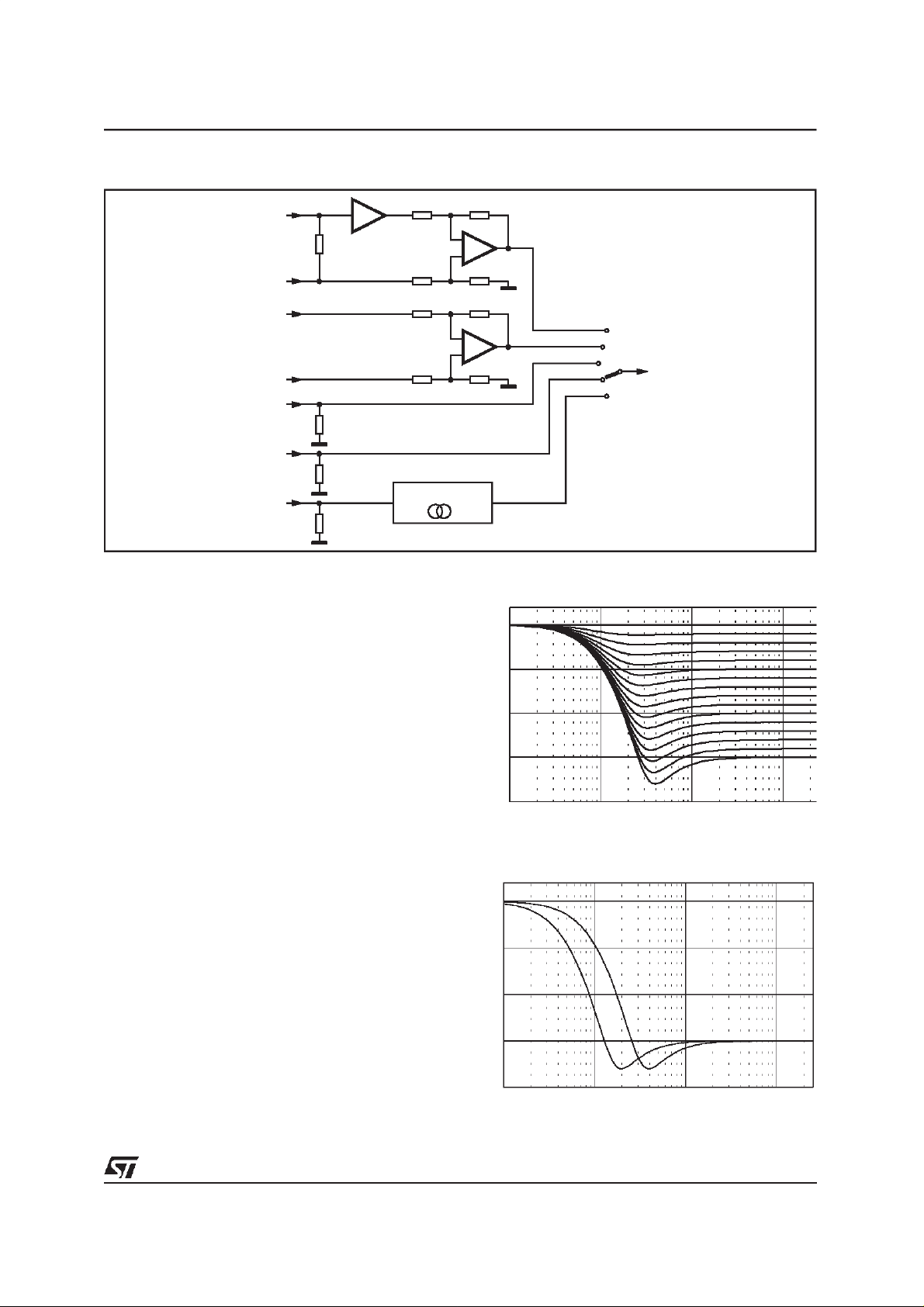
Figure 2. Inputstages
TDA7460N
CD
100K
CDGND
PHONE
PH_GND
CASSETTE
100K
AM
100K
MPX
100K
15K 15K
15K 15K
15K 15K
15K 15K
STEREODECODER
Mixing Stage
This stage offers the possibilityto mix the internal
beep or the phone signal to any other source.
Due to the fact that the mixing stage is also located behind the In-Gain stage fine adjustments
of the main source level can be donein this way.
-
+
-
+
IN GAIN
D97AU633A
Figure 3. Loudness Attenuation @ fc = 400Hz
(secondorder)
0.0
-5.0
Loudness
There are four parameters programmable in the
loudnessstage (see fig. 3, 4, 5):
- Attenuation
- Center Frequency
- LoudnessQ
- Flat Mode: in this mode the loudnessstageworks
asa 0 - 15dBattenuator.
Softmute
The digitally controlled softmute stage allows
muting/demuting the signal with a I
grammable slope. The mute process can either
be activated by the softmute pin or by the I
2
C bus pro-
2
bus. The slope is realized in a special S shaped
curve to mute slow in the critical regions (see figure 6).
For timing purposes the Bit 3 of the I
2
C bus output registeris set to 1 from the start of muting until the end of demuting.
-10.0
-15.0
-20.0
10.0 100.0 1.0K 10.0K
Figure 4. Loudness Center frequency @ Attn.
= 15dB (second order)
0.0
-5.0
-10.0
C
-15.0
-20.0
10.0 100.0 1.0K 10.0K
9/31
Page 10

TDA7460N
Figure 5. Loudness @ Attn.= 15dB, fc = 400Hz
(dB)
-5
-10
-15
-20
10 100 1,000 Hz
D98AU844
Softstep Volume
When volume level is changed often an audible
click appears at the output. The root cause of
those clicks could be either a DC offset before
the volume stage or the sudden change of the
envelope of the audio signal. With the Softstep
feature both kinds of clickscould be reduced to a
minimum and are no moreaudible(see figure 7).
Bass
There are three parameters programmable in the
bass stage (see figs 8, 9, 10,11):
Figure 6. Softmute Timing
1
EXT.
MUTE
+SIGNAL
REF
-SIGNAL
1
2
I
C
BUS
OUT
D97AU634
Note: Please notice that a startedMute actionis always terminated
and could not be interrupted by a change of the mute signal.
Time
Figure 7. SoftStep Timing
VOUT
2dB
1dB
- Attenuation
- Center Frequency (60, 70, 80 and 100Hz)
- Quality Factors (1, 1.25, 1.5 and 2)
DC Mode
In this mode the DC gain is increased by 4.4dB.
In addition the programmed center frequencyand
quality factor is decreased by 25% which can be
used to reach alternative center frequencies or
quality factors.
Treble
There are two parameters programmable in the
treblestage (see figs 12, 13):
- Attenuation
- Center Frequency (10, 12.5, 15 and17.5kHz).
Speaker Attenuator
Due to practicalaspects the stepsin the speaker
attenuators are not linear over the full range. At
attenuations more than 24dB the steps increase
from 1.5dB to 10dB (please see data byte specification).
10ms
-1dB
-2dB
Note: For steps more than 1dB the softstep mode should be
deactivated because it could generate a 1dB error during the
blend-time
Time
D97AU635
10/31
Page 11

TDA7460N
Figure 8. BassControl @ fc = 80Hz, Q = 1
15.0
10.0
5.0
0.0
-5.0
-10.0
-15.0
10.0 100.0 1.0K 10.0K
Figure 10. Bass Quality factors @ Gain =
14dB, fc = 80Hz
15.0
12.5
10.0
7.5
5.0
Figure 9. BassCenter@ Gain= 14dB, Q = 1
15.0
12.5
10.0
7.5
5.0
2.5
0.0
10.0 100.0 1.0K 10.0K
Figure 11. Bass normal and DC Mode@ Gain
= 14dB, fc = 80Hz
15.0
12.5
10.0
7.5
5.0
2.5
2.5
0.0
10.0 100.0 1.0K 10.0K
Figure 12. Treble Control@ fc = 17.5KHz
15.0
10.0
5.0
0.0
-5. 0
-10.0
-15.0
10.0 100.0 1.0K 10.0K
0.0
10.0 100.0 1.0K 10.0K
Note: In general the center frequency, Q and DC-mode can be set
independently. The exceptionfromthis ruleis themode(5/xx1111xx)
where the center frequency is set to 150Hz instead of 100Hz.
Figure 13. Treble CenterFrequencies
@ Gain = 14dB
15.0
12.5
10.0
7.5
5.0
2.5
0.0
10.0 100.0 1.0K 10.0K
11/31
Page 12

TDA7460N
STEREODECODERPART
No externalcomponentsnecessary
PLL with adjustment free fully integratedVCO
Automatic pilot dependent MONO/STEREO
switching
Very high suppression of intermodulation and
interference
ProgrammableRoll-Off compensation
ELECTRICAL CHARACTERISTICS
75KHz deviation, f = 1KHz. G
I = 6dB,Tamb =25°C; unlessotherwisespecified).
(V
S
= 9V; deemphasis time constant = 50µs, V
Dedicated RDS Softmute
Highcut and Stereoblend characterisctics pro-
grammablein a wide range
Internal Noiseblankerwith threshold controls
Multipath detector with programmable inter-
nal/external influence
2
C bus controlof all necessaryfunctions
I
MPX
= 500mV,
Symbol Parameter Test Condition Min. Typ. Max. Unit
IN MPX Input Level Input Gain = 3.5dB 0.5 1.25 VRMS
V
R
in
min Minimum Input Gain 1.5 3.5 4.5 dB
G
G
max
G
STEP
SVRR Supply Voltage Ripple Rejection V
α
Input Resistance 70 100 130 K
Max Input Gain 8.5 11 12.5 dB
Step Resolution 1.75 2.5 3.25 dB
= 100mv, f = 1khz 55 dB
ripple
Max Channel Separation 30 50 dB
THD Total Harmonic Distortion 0.02 0.3 %
S+N
Signal plus Noiseto Noise Ratio S = 2V
rms
80 91 dB
N
MONO/STEREOSWITCH
V
PTHST1
V
PTHST0
V
PTHMO1
V
PTHMO0
Pilot Threshold Voltage forStereo, PTH = 1 10 15 25 mV
Pilot Threshold Voltage forStereo, PTH = 0 15 25 35 mV
Pilot Threshold Voltage forMono, PTH = 1 7 12 17 mV
Pilot Threshold Voltage forStereo, PTH = 0 10 19 25 mV
Ω
PLL
∆f/f Capture Range 0.5 %
DEEMPHASISandHIGHCUT (5)
τHC50
τ
HC75
τ
HC50
τ
HC75
Deemphasis Time Constant Bit = 7, Subadr. 10 = 0
V
LEVEL >> VHCH
Deemphasis Time Constant Bit = 7, Subadr. 10 = 1
VLEVEL >> V
HCH
Highcut Time Constant Bit = 7, Subadr. 10 = 0
VLEVEL >> V
HCL
Highcut Time Constant Bit = 7, Subadr. 10 = 1
VLEVEL >> V
HCL
25 50 75
50 75 100
100 150 200
150 225 300
STEREOBLENDandHIGHCUT-CONTROL
REF5V Internal Reference Voltage 4.7 5 5.3 V
TC
REF5V
L
Gmin
Gmax Max. LEVEL Gain 8 10 12 dB
L
L
Gstep
VSBL
VSBL
VSBL
12/31
Temperature Coefficient 3300 ppm
Min. LEVEL Gain -1 0 +1 dB
LEVEL Gain Step Resolution 0.3 0.67 1.0 dB
min Min.Voltagefor Mono 29 33 37 %REF5V
Max. Voltage for Mono 54 58 62 %REF5V
max
Step Resolution 5.0 8.4 12 %REF5V
step
s
µ
s
µ
s
µ
s
µ
Page 13

TDA7460N
ELECTRICALCHARACTERISTICS
(continued)
Symbol Parameter Test Condition Min. Typ. Max. Unit
STEREOBLENDandHIGHCUT CONTROL
VHCH
VHCH
VHCH
VHCL
VHCL
Min.Voltage for NO Highcut 36 42 46 %REF5V
min
Max. Voltage for NO Highcut 62 66 70 %REF5V
max
step Step Resolution 5 8.4 12 %REF5V
Min. Voltage for FULL High cut 13 17 21 %VHCH
min
max Max.Voltagefor FULL Highcut 29 33 37 %VHCH
Carrierand harmonic suppressionat the output
19 Pilot Signal f = 19KHz 40 50 dB
α
38 Subcarrier f = 38KHz 75 dB
α
57 Subcarrier f = 57KHz 62 dB
α
76 Subcarrier f = 76KHz 90 dB
α
Intermodulation(Note1)
α2 Pilot Signal f
3f
α
= 10KHz; f
mod
= 13KHz; f
mod
= 1KHz; 65 dB
spur
= 1KHz; 75 dB
spur
Traffic Radio (Note 2)
57 Signal f = 57KHz 70 dB
α
SCA - SubsidiaryCommunicationsAuthorization(Note 3)
α67 Signal f = 67KHz 75 dB
ACI - Adjacent Channel Interference(Note 4)
114 Signal f = 114KHz 95 dB
α
190 Signal f = 190KHz 84 dB
α
Notes to the characteristics:
1. Intermodulation Suppression: measured with: 91% pilot signal; fm = 10kHz or 13kHz.
2. TrafficRadio (V.F.) Suppression: measured with: 91% stereo signal; 9% pilot signal; fm=1kHz; 5% subcarrier (f = 57kHz,
fm = 23Hz AM,m = 60%)
3. SCA ( Subsidiary Communications Authorization) measuredwith: 81% mono signal; 9% pilot signal; fm =1kHz; 10%SCA - subcarrier
( fs = 67kHz, unmodulated).
4. ACI ( Adjacent Channel Interference ) measured with: 90% mono signal; 9% pilot signal; fm =1kHz; 1% spurious signal
( fs = 110kHz or 186kHz, unmodulated).
5. By Design/Characterization but functionally guaranteed through dedicated test mode structure
13/31
Page 14

TDA7460N
NOISE BLANKER PART
tion, field-strenght)
internal 2nd order 140kHz high pass filter
programmabletriggerthreshold
very low offset current during hold time
four selectable pulse suppression times
additionalcircuits for trigger adjustment (devia-
ELECTRICALCHARACTERISTICS (continued)
Symbol Parameter Test Condition Min. Typ. Max. Unit
V
TR Trigger Threshold
V
TRNOISE
Noise Controlled Trigger
Threshold
VRECT Rectifier Voltage VMPX = 0mV 0.5 0.9 1.3 V
V
RECT DEV
deviation dependent
rectifier Voltage
VRECT FS Fieldstrength Controlled
Rectifier Voltage
0) All thresholds are measured using a pulse with TR=2µs, T
1) NBT represents the Noiseblanker-Byte bits D2; D0 for the noise blanker trigger threshold
2) NAT represents the Noiseblanker-Byte bitpair D4,D3 for the noise controlled trigger adjustment
3) OVD represents the Noiseblanker-Byte bit pair D7,D6 for the over deviation detector
4) FSC represents the Fieldstrength-Byte bit pair D1,D0 for the fieldstrength control
0) 1)
meas. with VPEAK = 0.9V NBT = 111 30 mVOP
NBT = 110 35 mVOP
NBT = 101 40 mV
NBT = 100 45 mV
NBT = 011 50 mV
NBT = 010 55 mV
NBT = 001 60 mVOP
NBT = 000 65 mVOP
2)
meas. with V
= 1.5V NCT = 00 260 mV
PEAK
NCT = 01 220 mV
NCT = 10 180 mV
NCT = 11 140 mV
V
MPX = 50mV; f = 150KHz 1.5 1.7 2.1 V
V
MPX = 100mV; f = 150KHz 2.2 2.5 2.9 V
3)
means. with
V
MPX = 800mV
(75KHz dev.)
OVD = 11 0.5 0.9(off) 1.3 V
OVD = 10 0.9 1.2 1.5 V
OVD = 01 1.7 2.0 2.3 V
OVD = 00 2.5 2.8 3.1 V
4)
means. with
V
= 0mV
MPX
V
<< V
LEVEL
SBL
(fully mono)
=2µs and TF=10µs.
HIGH
FSC = 11 0.5 0.9(off) 1.3 V
FSC = 10 1.0 1.3 1.6 V
FSC = 01 1.5 1.8 2.1 V
FSC = 00 2.0 2.3 2.6 V
OP
OP
OP
OP
OP
OP
OP
OP
OP
OP
OP
OP
14/31
V
IN
DC
D97AU636
V
OP
TRT
HIGH
T
F
Time
Page 15

Figure 14. Trigger Threshold vs. VPEAK
VTH
TDA7460N
260mV(00)
220mV(01)
180mV(10)
140mV(11)
MIN. TRIG. THRESHOLD
8 STEPS
65mV
30mV
0.9V
D97AU648
Figure 15. Deviation Controlled Trigger Adjustment
V
PEAK
(VOP)
2.8
2.0
1.2
0.9
D97AU649
20
32.5 45 75
NOISE
CONTROLLED
TRIG. THRESHOLD
V
1.5V
PEAK(V)
00
01
10
DETECTOR OFF (11)
DEVIATION(KHz)
Figure 16. Fieldstrength Controlled Trigger Adjustment
V
PEAK
MONO STEREO
»3V
NOISE
noisy signal good signal
D98AU863
ATC_SB OFF (11)
2.3V(00)
1.8V(01)
1.3V(10)
0.9V
E’
15/31
Page 16

TDA7460N
MULTIPATHDETECTOR
Internal19kHz bandpassfilter
Programmablebandpassand rectifier gain
ELECTRICALCHARACTERISTICS (continued)
Symbol Parameter Test Condition Min. Typ. Max. Unit
CMP Center frequency of Multipath-
f
Bandpass
G
BPMP
G
RECTMP
CHMP Rectifier Charge Current 1 µA
I
DISMP Rectifier DischargeCurrent 1.5 mA
I
Bandpass Gain bitsD2,D1configuration byte=00 6 dB
Rectifier Gain bitsD7,D6configuration byte=00 7.6 dB
stereodecoder locked on pilot
tone
bitsD
2,D1
bitsD
2,D1
bitsD
2,D1
bitsD
7,D6
bitsD
7,D6
Two pin solution fully independent usable for
externalprogramming
Selectable internal influence on Stereoblend
19 KHz
configuration byte=01 16 dB
configuration byte=10 12 dB
configuration byte=11 18 dB
configuration byte=01 4.6 dB
configuration byte=10 0 dB
Figure 17. Block diagram of the stereodecoder
MPX
100K
INGAIN
3.5 ... 11dB
STEP 2.5dB
INFILTER
LP
80KHz
4.th ORDER
PLL
+
PILOT-DET.
F19
F38
STEREO
NOISE BLANKER
HOLDN
D97AU762
DEMODULATOR
- PLOT
CANC
- ROLL-OFF
- LP 25KHz
COMP.
SB CONTROL
DEEMPHASIS
+ HIGHCUT
t=50 or 75µs
HC
CONTROL
REF 5V
VSBL
MPINFL
-
LEVEL INTERN
MULTIPATH
DETECTOR
D
A
LEVEL INPUT
LP 2.2KHZ
1.th ORDER
GAIN 0..10dB
FM_L
FM_R
VHCCH
VHCCL
LEVEL
MPIN
MPOUT
16/31
Page 17

TDA7460N
DESCRIPTIONOFSTEREODECODER
The stereodecoder part of the TDA7460N (see
Fig. 17) contains all functions necessary to demodulate the MPX signal like pilot tone dependent MONO/STEREO switching as well as
”stereoblend”and ”highcut”functions.
Adaptations like programmable input gain, roll-off
compensation, selectable deemphasis time constant and a programmable fieldstrength input allow to use different IF devices.
StereodecoderMute
The TDA7460N has a fast and easy to control
RDS mute function which is a combinationof the
audioprocessor softmute and the high-ohmic
mute of the stereodecoder. If the stereodecoder
is selected and a softmute command is sent (or
activated through the SM pin) the stereodecoder
will be set automaticallyto the high-ohmic mute
condition after the audio signal has been softmuted.
Hence a checking of alternate frequencies could
be performed. To release the system from the
mute condition simply the unmutecommand must
be sent: the stereodecoder is unmuted immediately and the audioprocessor is softly unmuted.
Fig. 18 shows the output signal V
as well as the
O
internal stereodecoder mute signal. This influence of Softmute on the stereodecodermute can
be switched off by setting bit 3 of the Softmute
byte to ”0”. A stereodecoder mute command (bit
0, stereodecoder byte set to ”1”) will set the
stereodecoder in any case independently to the
high-ohmicmute state.
If any other source than the stereodecoderis selected the decoder remains muted and the MPX
pin is connectedto Vref to avoid any dischargeof
the couplingcapacitor through leakage currents.
Input Stages
The Ingain stage allows to adjust the MPX signal
to a magnitude of about 1Vrms internally which is
the recommended value. The 4.th order input filter has a corner frequency of 80kHz and is used
to attenuatespikes and noise and acts as an antialiasing filter for the following switch capacitor filters.
Figure 18. Signals during stereodecoder’s
softmute
SOFTMUTE
COMMAND
t
STD MUTE
t
V
O
D97AU638
t
lowpass behaviour of the tuner section. If the
tuner attenuation at 38kHz is in a range from
20.2% to 31% the TDA7460N needs no external
network before the MPX pin. Within this range an
adjustment to obtain at least 40dB channel separation is possible.
The bits for this adjustment are located together
with the fieldstrength adjustment in one byte. This
gives the possibility to perform an optimization
step during the production of the carradio where
the channel separation and the fieldstrength control are trimmed.
Deemphasisand Highcut.
The lowpass filter for the deemphasis allows to
choose between a time constant of 50µs and
75µs (bit D7, Stereodecoderbyte).
The highcut control range will be in both cases
t
HC
=2⋅t
. Inside the highcut control range
Deemp
(between VHCH and VHCL) the LEVEL signal
is converted into a 5 bit word which controls the
lowpasstime constant between t
Deemp
...3 ⋅ t
Deemp
There by the resolution will remain always 5 bits
independently of the absolute voltage range between the VHCHand VHCL values.
The highcut function can be switched off by I2C
bus (bit D7, Fieldstrengthbyte set to ”0”).
.
Demodulator
In the demodulator block the left and the right
channel are separated from the MPX signal. In
this stage also the 19 kHz pilot tone is cancelled.
For reaching a high channel separation the
TDA7460N offers an I2C bus programmable rolloff adjustment which is able to compensate the
PLL and Pilot Tone Detector
The PLL has the task to lock on the 19kHz pilotone during a stereo transmission to allow a correct demodulation. The included detector enables
the demodulation if the pilot tone reaches the selected pilottone threshold VPTHST. Two different
thresholdsare available. The detectoroutput (signal STEREO, see block diagram) can be checked
17/31
Page 18

TDA7460N
by reading the status byte of the TDA7460N via
I2C bus.
FieldstrengthControl
The fieldstrength input is used to control the high
cut and the stereoblend function. In addition the
signal can be also used to control the noiseblanker thresholds.
LEVEL Input and Gain
To suppress undesired high frequency modulation on the highcut and stereoblend function the
LEVEL signal is lowpass filtered firstly. The filter
is a combination of a 1st order RC lowpass at
53kHz (working as anti-aliasing filter) and a 1storder switched capacitor lowpass at 2.2kHz. The
second stage is a programmable gain stage to
adapt the LEVEL signal internally to different IF.
The gain is widely programmable in 16 steps
from 0dB to 10dB (step = 0.67dB). These 4 bits
are located together with the Roll-Off bits in the
”Stereodecoder Adjustment” byte to simplify a
possible adaptation during the production of the
carradio.
StereoblendControl
The stereoblend control block converts the internal LEVEL voltage (LEVEL INTERN) into an demodulatorcompatible analog signal which is used
to control the channel separation between 0dB
and the maximum separation. Internally this control range has a fixed upper limit which is the internal reference voltage REF5V. The lower limit
can be programmed to be 33%, 42%, 50% or
58% of REF5V (see fig. 20).
To adjust the external LEVEL voltage to the internal range two values must be defined:the LEVEL
Figure 19. Internal stereoblendcharacteristics
gain L
and VSBL. To adjust the voltage where
G
the full channel separation is reached (VST) the
LEVEL gain L
has to be defined. The following
G
equation can be usedto estimatethe gain:
=
L
G
Field strength voltage [STEREO]
REF5V
The gain can be programmed through 4 bits in
the ”Stereodecoder-Adjustment”byte.
The MONO voltage VMO (0dB channel separation) can be choosen selecting 33, 42, 50 or 58%
of REF5V.
All necessary internal reference voltages like
REF5V are derived from a bandgap circuit.
Therefore they have a temperature coefficient
near zero.This is useful if the fieldstrengthsignal
is also temperaturecompensated.
But most IF devicesapplya LEVELvoltagewith a
TC of 3300ppm. The TDA7460N offers this TC
for the reference voltages, too. The TC is selectable with bit D7 of the ”stereodecoder adjustment” byte.
Figure 20. Relation between internal and external LEVEL voltageand setup of Stereoblend
INTERNAL
VOLTAGES
REF 5V
18/31
VSBL
SETUP OF VST
LEVEL INTERN
LEVEL
VSTVMO
t
FIELDSTRENGHT VOLTAGE
INTERNAL
VOLTAGES
REF 5V
VSBL
58%
50%
42%
33%
D97AU639
SETUP OF VMO
VMO FIELDSTRENGHT VOLTAGE
LEVEL INTERN
VST
t
Page 19

TDA7460N
Highcut Control
The highcut control setup is similar to the
stereoblend control setup : the starting point
VHCH can be set with 2 bits to be 42, 50, 58 or
66% of REF5V whereas the range can be set to
be 17or 33% of VHCH(see fig. 21).
Figure 21. Highcut characteristics
LOWPASS
TIME CONSTANT
3•τ
Deemp
τ
Deemp
D97AU640
FIELDSTRENGHTVHCHVHCL
FUNCTIONAL DESCRIPTION OF THE NOISEBLANKER
In the automotive environment the MPX signal is
disturbed by spikes produced by the ignition and
for example the wiper motor. The aim of the
noiseblanker part is to cancel the audible influence of the spikes. Therefore the output of the
stereodecoder is held at the actual voltage for
40µs.
In a first stage the spikes must be detected but to
avoid a wrong triggering on high frequency
(white) noise a complex trigger control is implemented. Behind the triggerstage a pulse former
generates the ”blanking” pulse. To avoid any
crosstalk to the signalpath the noiseblanker is
suppliedby hisown biasing circuit.
TriggerPath
The incoming MPX signal is highpass filtered,
amplified and rectified. This second order highpass-filter has a corner frequency of 140kHz. The
rectified signal, RECT, is lowpass filtered to generate a signal called PEAK. Also noise with a frequency 140kHz increases the PEAK voltage. The
PEAK voltage is fed to a threshold generator,
which adds to the PEAK voltage a DC dependent threshold VTH. Both signals, RECT and
PEAK+VTH are fed to a comparator which triggers a re-triggerable monoflop. The monoflop’s
output activates the sample-and-hold circuits in
the signalpathfor 40µs.
The block diagram of the noiseblanker is given in
fig.22.
Automatic Noise ControlledThreshold Adjustment (ATC)
There are mainly two independentpossibilities for
programmingthe trigger threshold:
a the low thresholdin 8 steps(bits D0 to D2 of
the noiseblankerbyte)
b the noise adjusted thresholdin 4 steps
(bits D3 andD4 of the noiseblankerbyte,
see fig. 14).
The low threshold is active in combination with a
good MPX signal without any noise; the PEAK
voltage is less than 1V. The sensitivity in this operation is high.
If the MPX signal is noisy the PEAK voltage increases due to the higher noise, which is also
rectified. With increasing of the PEAK voltage the
trigger threshold increases, too. This particular
gain is programmable in 4 steps (see fig. 14).
Figure 22. Block diagram of the noiseblanker
MPX
HIGH PASS
RECTIFIER
LOWPASS
D98AU861
RECT
+
-
VTH
+
PEAK
+
MONOFLOP HOLDN
THRESHOLD
GENERATOR
ADDITIONAL
THRESHOLD
CONTROL
19/31
Page 20

TDA7460N
Automatic Threshold Control
Besides the noise controlled threshold adjustment there is an additional possibility for influencing the trigger threshold. It is depending on the
stereoblendcontrol.
The point wherethe MPX signal starts to become
noisy is fixed by the RF part. Therefore also the
starting point of the normal noise-controlled trigger adjustment is fixed (fig. 16). In some cases
the behaviour of the noiseblanker can be improved by increasing the threshold even in a region of higher fieldstrength. Sometimes a wrong
triggering occures for the MPXsignal often shows
distortion in this range which can be avoided
even if using a low threshold.
Because of the overlap of this range and the
range of the stereo/monotransition it can be controlled by stereoblend. This threshold increase is
programmable in 3 steps or switched off with bits
D0 and D1 of the fieldstrengthcontrol byte.
Over DeviationDetector
If the system is tuned to stations with a high deviation the noiseblanker can trigger on the higher
frequencies of the modulation. To avoid this
wrong behaviour, which causes noise in the output signal,the noiseblankeroffers a deviation dependent threshold adjustment.
By rectifying the MPX signal a further signal representing the actual deviation is obtained. It is
used to increase the PEAK voltage. Offset and
gain of this circuit are programmable in 3 steps
with the bits D6 andD7 of thestereodecoderbyte
(the first step turns off thedetector,see fig. 15).
FUNCTIONAL DESCRIPTION OF THE MULTIPATH DETECTOR
Using the internal detector the audibleeffects of a
multipath condition can be minimized.A multipath
condition is detected by rectifying the 19kHz
spectrumin thefieldstrengthsignal.
Selecting the ”internal influence” in the configuration byte, the channel separation is automatically
reduced during a multipath condition according to
the voltageappearing at theMPOUT pin.
To obtain a optimal performance an adaptationis
necessary.Thereforethe gain of the 19kHzbandpass is programmablein four steps as well as the
rectifier gain. The attack and decay times can be
set by the external capacitorvalue.
TEST MODE
During the test mode which can be activated by
setting bit D0 of the testing byte and bit D5 of the
subaddress byte to ”1” several internal signals
are available at the CASSR pin. During this
mode the input resistance of 100kOhm is disconnected from the pin. The internalsignalsavailable
are shown in thesoftware specification.
Figure 23. Block diagram of the Multipath Detector
LEVEL
DC=1µ
MP ENABLE
RECTIFIER
GAIN
2 BITS
D98AU862
MPIN
BANDPASS
19KHz
15K
GAIN
2 BITS
VDD
-
MPOUT
220nF
to SB
int. INFLUENCE
TO PHONE_GND - APR
20/31
Page 21

Figure 24. ApplicationExample 1 (with Phone input)
TDA7460N
V
S
+V
CC
=
100nF
9V
100nF
CASS R
100nF
CASS L
100nF
CDR
22µF
CDG
100nF
CDL
220nF
PHGND
220nF
PHONE
CASS R
CASS L
CDR
CDG
CDL
PHONE_GND
PHONE
TDA7460
Figure 25. ApplicationExample 2 (with multipath)
CREF
OUTLF
OUTLF
OUTRF
OUTRF
OUTLR
OUTLR
OUTRR
MPX
AM
SDA
SCL
SMUTE
LEVEL
GND
10µF
220nF
220nF
D97AU643A
OUTRR
MPX
AM
SDA
SCL
SMUTE
LEVEL
V
S
+V
CC
100nF
100nF
100nF
22µF
100nF
47nF
100nF
CASS R
CASS L
MPOUT
=
9V
CASS R
CASS L
CDR
CDG
CDL
UNWEIGHTED
LEVEL
CDR
CDG
CDL
MPIN
TDA7460
CREF
OUTLF
OUTRF
OUTLR
OUTRR
MPX
AM
SDA
SCL
SMUTE
LEVEL
GND
10µF
220nF
220nF
D97AU645A
OUTLF
OUTRF
OUTLR
OUTRR
MPX
AM
SDA
SCL
SMUTE
LEVEL
21/31
Page 22

TDA7460N
I2C BUS INTERFACE DESCRIPTION
Interface Protocol
The interfaceprotocol comprises:
-a start condition (S)
/ write transmission)
-a subaddressbyte
-a sequence of data(N-bytes+ acknowledge)
-a stop condition(P)
-a chip address byte (the LSB bit determinesread
CHIP ADDRESS
MSB LSB MSB LSB MSB LSB
S1000110R/WACK ACK ACKP
D97AU627
S = Start
ACK = Acknowledge
AZ = AutoZero-Remain
SUBADDRESS DATA 1 to DATA n
XI
AZ T A3 A2 A1 A0 DATA
Auto increment
If bit I in the subaddress byte is set to ”1”, the
autoincrementof the subaddressis enabled.
T = Testing
I = Autoincrement
P = Stop
MAX CLOCK SPEED 500kbits/s
The transmitted data is automatically updated after each ACK.
Transmission can be repeated without new chip
TRANSMITTED DATA (send mode)
MSB LSB
XXXXSTSMXX
SM = Soft mute activated
ST = Stereo
X = Not Used
address.
SUBADDRESS (receive mode)
MSB LSB FUNCTION
X AZ T I A3A2A1A0
Input selector
0
0
0
0
0
0
0
0
1
1
1
1
1
1
1
1
0
0
0
0
1
1
1
1
0
0
0
0
1
1
1
1
0
0
1
1
0
0
1
1
0
0
1
1
0
0
1
1
0
Loudness / Auto-Zero
1
Volume
0
Softmute / Beep
1
Bass / Treble Attenuator
0
Bass / Treble Configuration
1
Speaker attenuator LF
0
Speaker attenuator LR
1
Speaker attenuator RF
0
Speaker attenuator RR / Blanktime adjust
1
Stereodecoder
0
Noiseblanker
1
Fieldstrength Control
0
Configuration
1
Stereodecoder Adjustment
0
Testing
1
T = Testmode
I = Autoincrement
AZ = Auto Zero Remain
X = notused
22/31
Page 23

DATA BYTE SPECIFICATION
Input Selector
MSB LSB FUNCTION
D7 D6 D5 D4 D3 D2 D1 D0
Source Selector
CD
0
0
0
0
1
1
1
1
0
1
1
0
0
1
0
0
:
1
1
For example to select the CD input in quasi-differential mode with gain of 8dB the Data Byte is: 0/01111000
0
0
:
1
1
0
1
:
0
1
0
0
1
1
0
0
1
1
0
0
1
1
1
1
0
0
0
Cassette
1
Phone
0
AM
1
Stereo Decoder
0
Input FM
1
Mute
0
AC inputs
1
CD Mode
CD Full-differential
CD Quasi-diff
AM/FM Mode
AM mono
1
AM stereo
1
AM through Stereodecoder
0
FM- Stereodecoder
0
In-Gain
14dB
12dB
:
2dB
0dB
TDA7460N
Loudness
MSB LSB LOUDNESS
D7 D6 D5 D4 D3 D2 D1 D0
Attenuation
0dB
0
0
:
1
1
0
1
0
1
0
1
1 must be ”1”
Note: The attenuation is specified at high frequencies. Around the center frequency the value is different depending on theprogrammed
attenuation(see Loudness frequency response).
0
0
:
1
1
0
0
:
1
1
0
-1dB
1
:
:
-14dB
0
-15dB
1
Filter
on
off (flat)
Center Frequency
200Hz
400Hz
LoudnessQ
low (1
normal (2
st
order)
nd
order)
23/31
Page 24

TDA7460N
Mute, Beep and Mixing
MSB LSB MUTE/BEEP/MIXING
D7 D6 D5 D4 D3 D2 D1 D0
Mute
Enable Softmute
0
Disable Softmute
1
0
0
1
0
1
0
1
0
0
0
1
1
Note: for more information tothe Stereodecoder-Softmute-Influence please refer to the stereodecoder description.
0
1
0
1
1
1
0
1
0
1
Mute time =0.48 ms
Mute time =0.96 ms
Mute time =40.4 ms
Mute time =324 ms
Stereo Decoder Softmute Influence= off
Stereo Decoder Softmute Influence= on
Beep
Beep Frequency = 600Hz
Beep Frequency = 1.2KHz
Mixing
Mix-Source = Beep
Mix-Source = Phone
Full Mix Signal
Source -12dB + Mix-Signal -2.5dB
Source -6dB + Mix-Signal -6dB
Full Source
Volume
MSB LSB ATTENUATION
D7 D6 D5 D4 D3 D2 D1 D0
Gain/Attenuation
+32dB
0
0
:
0
0
0
:
0
0
0
:
1
1
0
1
Note: It is not recommended to use a gain more than 20dB for system performance reason. In general, the max. gain should be limited by
softwareto the maximum value,which is neededfor the system.
0
0
:
0
0
0
:
0
1
1
:
1
1
0
0
:
0
0
0
:
1
0
0
:
0
0
0
0
:
1
1
1
:
1
0
0
:
1
1
0
0
:
1
1
1
:
1
0
0
:
1
1
0
0
:
0
0
1
:
1
0
0
:
1
1
0
+31dB
1
:
:
+20dB
0
+19dB
1
+18dB
0
:
:
+1dB
1
0dB
0
- 1dB
1
:
:
-78dB
0
-79dB
1
Softstep
Softstep Volume = off
Softstep Volume = on
24/31
Page 25

TDA7460N
Bass & Treble Attenuation
MSB LSB BASS & TREBLEATTENUATION
D7 D6 D5 D4 D3 D2 D1 D0
Treble Steps
-14dB
0
0
:
0
0
1
1
:
1
1
0
0
:
0
0
1
1
:
1
1
For example 12dB Trebleand -8dB Bass give the following DATA BYTE: 0 0 1 1 1 0 0 1.
0
0
:
1
1
1
1
:
0
0
0
0
:
1
1
1
1
:
0
0
0
1
:
0
1
1
0
:
1
0
0
0
:
1
1
1
1
:
0
0
0
0
:
1
1
1
1
:
0
0
0
1
:
0
1
1
0
:
1
0
-12dB
:
-2dB
0dB
0dB
+2dB
:
+12dB
+14dB
Bass Steps
-14dB
-12dB
:
-2dB
0dB
0dB
+2dB
:
+12dB
+14dB
Bass & Treble Filter Characteristics
MSB LSB BASS & TREBLEFILTER
D7 D6 D5 D4 D3 D2 D1 D0
Treble
Center Frequency = 10 KHz
0
0
1
1
0
0
1
1
1
0
0
1
1
0
1
1 must be ”1”
For example Treble center frequency = 15kHz, Bass center frequency = 100Hz, Bass Q = 1 and DC = 0dB give the following DATA BYTE: 1
0001110
1
0
1
0
1
1
0
1
0
1
1
0
Center Frequency = 12.5 KHz
1
Center Frequency = 15 KHz
0
Center Frequency = 17.5 KHz
1
Bass
Center Frequency = 60 Hz
Center Frequency = 70 Hz
Center Frequency = 80 Hz
Center Frequency = 100Hz
Center Frequency = 150Hz
Quality factor = 1
Quality factor = 1.25
Quality factor = 1.5
Quality factor = 2
DC-Gain = 0dB
DC-Gain =±4.4dB
25/31
Page 26

TDA7460N
Speaker Attenuation (LF, LR, RF, RR)
MSB LSB
D7 D6 D5 D4 D3 D2 D1 D0
0
0
:
1
0
0
1
1
0
0
1
1
11
0
0
1
1
0
1
0
1
0
0
:
0
0
0
0
0
0
0
0
0
1
0
0
:
1
1
1
1
1
1
1
1
1
0
0
:
0
1
1
1
1
1
1
1
1
0
0
:
1
0
0
0
0
1
1
1
1
Attenuation
0dB
0
-1dB
1
:
:
-23dB
1
-24.5dB
0
-26dB
1
-28dB
0
-30
1
-32dB
0
-35dB
1
-40dB
0
-50dB
1
Speaker Mute
Must be ”1” (except RR speaker; see below)
Blank Time adj. (only at RR speaker)
38µs
25.5µs
32µs
22µs
26/31
Page 27

Stereodecoder
MSB LSB FUNCTION
D7 D6 D5 D4 D3 D2 D1 D0
01STD Unmuted
STD Muted
0
0
1
1
1 must be ”1”
1
1
0
1
0
1
0
1
0
1
0
1
IN-Gain 11dB
IN-Gain 8.5dB
IN-Gain 6dB
IN-Gain 3.5dB
Forced MONO
MONO/STEREO switch automatically
Pilot Threshold HIGH
Pilot Threshold LOW
Deemphasis 50µs
Deemphasis 75µs
TDA7460N
Noiseblanker
MSB LSB FUNCTION
D7 D6 D5 D4 D3 D2 D1 D0
Low Threshold 65mV
0
0
0
0
1
1
1
1
0
0
1
1
0
1
0
0
1
1
0
1
0
1
0
1
0
1
0
0
1
1
0
0
1
1
0
Low Threshold 60mV
1
Low Threshold 55mV
0
Low Threshold 50mV
1
Low Threshold 45mV
0
Low Threshold 40mV
1
Low Threshold 35mV
0
Low Threshold 30mV
1
Noise Controlled Threshold 320mV
Noise Controlled Threshold 260mV
Noise Controlled Threshold 200mV
Noise Controlled Threshold 140mV
Noise blanker OFF
Noise blanker ON
Over deviation Adjust 2.8V
Over deviation Adjust 2.0V
Over deviation Adjust 1.2V
Over deviation Detector OFF
27/31
Page 28

TDA7460N
FieldstrengthControl
MSB LSB FUNCTION
D7 D6 D5 D4 D3 D2 D1 D0
Noiseblanker Field strengthAdj 2.3V
0
0
1
1
0
0
1
1
0
0
1
1
1
0
0
1
0
1
0
1
0
1
0
1
0
Noiseblanker Field strengthAdj 1.8V
1
Noiseblanker Field strengthAdj 1.3V
0
Noiseblanker Field strengthAdj OFF
1
VSBL at 33% REF5V
VSBL at 42% REF5V
VSBL at 50% REF5V
VSBL at 58% REF5V
VHCH at 42% REF 5V
VHCH at 50% REF 5V
VHCH at 58% REF 5V
VHCH at 66% REF 5V
VHCL at 17% VHCH
VHCL at 33% VHCH
High cut OFF
High cut ON
Configuration
MSB LSB FUNCTION
D7 D6 D5 D4 D3 D2 D1 D0
Noise Rectifier Discharge Resistor
R = infinite
0
0
1
1
0
0
1
1
0
1
0
1
0
0
1
1
0
1
0
1
0
1
0
1
0
R = 56kΩ
1
R = 33k
0
1
Ω
R =18k
Ω
Multipath Detector Bandpass Gain
6dB
16dB
12dB
18dB
Multipath Detector internal influence
ON
OFF
Multipath/function selected (MPIN, MPOUT)
Additional input selected (Phone)
Multipath Detector Reflection Gain
Gain = 7.6dB
Gain = 4.6dB
Gain = 0dB
OFF
28/31
Page 29

StereodecoderAdjustment
MSB LSB FUNCTION
D7 D6 D5 D4 D3 D2 D1 D0
Roll-Off Compensation
not allowed
0
0
0
:
1
:
1
0
0
0
:
1
0
1
0
0
0
:
1
0
0
1
:
1
0
1
0
:
1
0
0
1
:
0
:
1
0
20.2%
1
21.9%
0
:
:
25.5%
0
:
:
31.0%
1
LEVEL Gain
0dB
0.66dB
1.33dB
:
10dB
Temperature compensation at LEVEL input
TC = 0
TC = 16.7mV/K (3300ppm)
Testing
TDA7460N
MSB LSB FUNCTION
D7 D6 D5 D4 D3 D2 D1 D0
Stereodecoder test signals
0
OFF
1
Test signals enabled if bit D5 of the subaddress
(test mode bit)is set to ”1”, too
0
1
0
0
0
0
0
0
0
0
1
1
1
1
1
1
1
1
0
1
0
1
Note :This byteisused fortesting or evaluationpurposes only andmust notbesetto othervalues thanthedefault ”11111110”in theapplication!
0
0
0
0
1
1
1
1
0
0
0
0
1
1
1
1
0
0
1
1
0
0
1
1
0
0
1
1
0
0
1
1
0
1
0
1
0
1
0
1
0
1
0
1
0
1
0
1
External Clock
Internal Clock
Testsignals at CASS_R
VHCCH
Level intern
Pilot magnitude
VCOCON; VCO Control Voltage
Pilot threshold
HOLDN
NB threshold
F228
VHCCL
VSBL
not used
not used
PEAK
not used
REF5V
not used
VCO
OFF
ON
Audioprocessor test mode
only if bit D5 of the subaddress
(test mode bit)is set to ”1”
OFF
29/31
Page 30

TDA7460N
DIM.
MIN. TYP. MAX. MIN. TYP. MAX.
A 2.35 2.65 0.093 0.104
A1 0.1 0.3 0.004 0.012
B 0.33 0.51 0.013 0.020
C 0.23 0.32 0.009
D 12.6 13 0.496 0.512
E 7.4 7.6 0.291 0.299
e 1.27 0.050
H 10 10.65 0.394 0.419
h 0.25 0.75 0.010 0.030
L 0.4 1.27 0.016 0.050
K0°(min.)8°(max.)
mm inch
0.013
OUTLINE AND
MECHANICAL DATA
SO20
B
e
D
1120
110
L
hx45°
A
K
A1
C
H
E
SO20MEC
30/31
Page 31

TDA7460N
Information furnished is believed to be accurate and reliable. However, STMicroelectronics assumes no responsibility for the consequences
of use of such information nor for any infringement of patents or other rights of third parties which may result from its use. No license is
granted by implication or otherwise under any patentor patent rights of STMicroelectronics. Specification mentioned in this publication are
subject to change without notice. This publicationsupersedes and replaces all information previously supplied. STMicroelectronics products
are not authorized for use as critical components in life support devices or systems without express written approval of STMicroelectronics.
The ST logois a registeredtrademark of STMicroelectronics
2000 STMicroelectronics – Printed in Italy – All Rights Reserved
STMicroelectronics GROUP OF COMPANIES
Australia - Brazil - China- Finland - France - Germany - Hong Kong - India - Italy - Japan - Malaysia - Malta - Morocco -
Singapore - Spain - Sweden - Switzerland- United Kingdom - U.S.A.
http://www.st.com
31/31
 Loading...