

Page 1

INTEGRATED CIRCUITS
DATA SH EET
TDA7073A; TDA7073AT
Dual BTL power driver
Product specification
Supersedes data of 1994 July
File under Integrated Circuits, IC01
1999 Aug 30
Page 2
Philips Semiconductors Product specification
Dual BTL power driver TDA7073A; TDA7073AT
FEATURES
• No external components
• Very high slew rate
• Single power supply
• Short-circuit proof
GENERAL DESCRIPTION
The TDA7073A/AT aredual power driver circuits in a BTL
configuration, intended for use as a power driver for servo
systems with a single supply. They are specially designed
for compact disc players and are capable of driving focus,
tracking, sled functions and spindle motors.
• High output current (0.6 A)
• Wide supply voltage range
• Low output offset voltage
• Suited for handling PWM signals up to 176 kHz
• ESD protected on all pins.
Missing Current Limiter (MCL)
A MCL protection circuit is built-in. The MCL circuit is
activated when the difference in current between the
output terminal of each amplifier exceeds 100 mA (typical
300 mA). This level of 100 mA allows for headphone
applications (single-ended).
QUICK REFERENCE DATA
SYMBOL PARAMETER CONDITIONS MIN. TYP. MAX. UNIT
V
P
G
v
I
P
positive supply voltage range 3.0 5.0 18 V
voltage gain 32.5 33.5 34.5 dB
total quiescent current VP=5V; RL=∞−816mA
SR slew rate − 12 − V/µs
I
I
f
O
bias
co
output current −−0.6 A
input bias current − 100 300 nA
cut-off frequency −3dB − 1.5 − MHz
ORDERING INFORMATION
PACKAGE
TYPE NUMBER
NAME DESCRIPTION VERSION
TDA7073A DIP16 plastic dual in-line package; 16 leads (300 mil); long body SOT38-1
TDA7073AT SO16 plastic small outline package; 16 leads; body width 7.5 mm SOT162-1
1999 Aug 30 2
Page 3
Philips Semiconductors Product specification
Dual BTL power driver TDA7073A; TDA7073AT
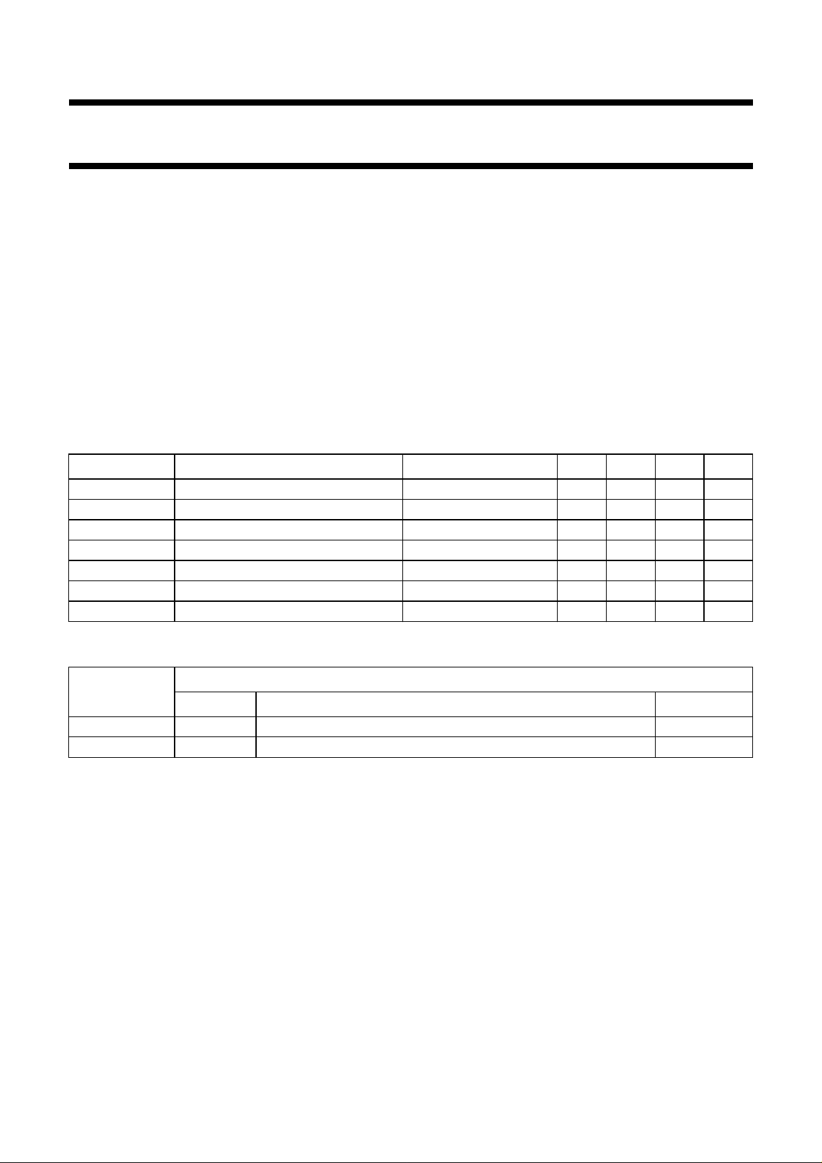
BLOCK DIAGRAM
V
P
handbook, full pagewidth
positive input 1
negative input 1
positive input 2
negative input 2
2
1
TDA7073A
TDA7073AT
6
7
5
Ι
SHORT - CIRCUIT AND
THERMAL PROTECTION
I – i
ΙΙ
16I + i
13I – i
12
9I + i
positive output 1
negative output 1
negative output 2
positive output 2
10
ground 2
14
ground 1
Fig.1 Block diagram.
1999 Aug 30 3
3, 4, 8, 11, 15
MCD382 - 1
n.c.
Page 4
Philips Semiconductors Product specification
Dual BTL power driver TDA7073A; TDA7073AT
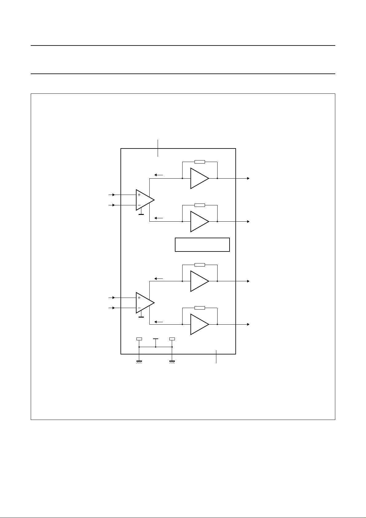
PINNING
SYMBOL PIN DESCRIPTION
IN1− 1 negative input 1
IN1+ 2 positive input 1
n.c. 3 not connected
n.c. 4 not connected
V
P
5 positive supply voltage
IN2+ 6 positive input 2
IN2− 7 negative input 2
n.c. 8 not connected
OUT2+ 9 positive output 2
GND2 10 ground 2
n.c. 11 not connected
OUT2− 12 negative output 2
OUT1− 13 negative output 1
GND1 14 ground 1
n.c. 15 not connected
OUT1+ 16 positive output 1
handbook, halfpage
1
IN1–
IN1+
2
3
n.c.
4
n.c.
V
IN2 +
IN2 –
n.c.
P
TDA7073A
TDA7073AT
5
6
7
8
MCD381
Fig.2 Pin configuration.
16
15
14
13
12
11
10
9
OUT1+
n.c.
GND1
OUT1 –
OUT2 –
n.c.
GND2
OUT2 +
FUNCTIONAL DESCRIPTION
The TDA7073A/AT are dual power driver circuits in a BTL
configuration, intended for use as a power driver for servo
systemswith a single supply. Theyareparticular designed
for compact disc players and are capable of driving focus,
tracking, sled functions and spindle motors.
Because of the BTL configuration, the devices can supply
a bi-directional DC current in the load, with only a single
supply voltage. The voltage gain is fixed by internal
feedback at 33.5 dB and the devices operate in a wide
supply voltage range (3 to 18 V). The devices can supply
a maximum output current of 0.6 A. The outputs can be
short-circuited over the load, to the supply and to ground
at all input conditions. The differential inputs can handle
common mode input voltages from ground level up to
(VP− 2.2 V with a maximum of 10 V). The devices have a
very high slew rate. Due to the large bandwidth, they can
handle PWM signals up to 176 kHz.
1999 Aug 30 4
Page 5
Philips Semiconductors Product specification
Dual BTL power driver TDA7073A; TDA7073AT
LIMITING VALUES
In accordance with the Absolute Maximum System (IEC 134).
SYMBOL PARAMETER CONDITIONS MIN. MAX. UNIT
V
P
I
ORM
I
OSM
P
tot
T
stg
T
vj
T
sc
Note
1. The outputs can be short-circuited over the load, to the supply and to ground at all input conditions.
positive supply voltage range − 18 V
repetitive peak output current − 1A
non repetitive peak output current − 1.5 A
total power dissipation
TDA7073A T
TDA7073AT T
<25°C − 2.5 W
amb
<25°C − 1.32 W
amb
storage temperature range −55 +150 °C
virtual junction temperature − 150 °C
short-circuit time see note 1 − 1hr
THERMAL CHARACTERISTICS
SYMBOL PARAMETER CONDITIONS VALUE UNIT
R
th (j-a)
from junction to ambient
TDA7073A in free air; note 1 50 K/W
TDA7073AT in free air; note 2 95 K/W
Notes
1. TDA7073A: V
P
=2×0.76 W = 1.52 W; T
tot
= 5 V; RL=8Ω; The typical voltage swing = 5.8 V and V
P
amb (max)
= 150 − 1.52 × 50 = 74 °C.
2. TDA7073AT: VP= 5 V; RL=16Ω; typical voltage swing = 5.8 V and V
P
=2×0.38 W = 0.76 W; T
tot
amb (max)
= 150 − 0.76 × 95 = 77 °C.
is 2.1 V therefore IO= 0.36 A and
loss
is 2.1 V therefore IO= 0.18 A and
loss
1999 Aug 30 5
Page 6

Philips Semiconductors Product specification
Dual BTL power driver TDA7073A; TDA7073AT
CHARACTERISTICS
VP= 5 V; f = 1 kHz; T
SYMBOL PARAMETER CONDITIONS MIN. TYP. MAX. UNIT
V
P
I
ORM
I
P
∆V
OUT
THD total harmonic distortion
G
v
V
no(rms)
B bandwidth −−1.5 MHz
SVRR supply voltage ripple rejection note 4 38 55 − dB
∆V
V
I(CM)
16-13,12-9
DC output offset voltage RS= 500 Ω−−100 mV
CMRR DC common mode rejection ratio note 6 − 100 − dB
Z
I
I
bias
α channel separation 40 50 − dB
∆GV channel unbalance −−1dB
SR slew rate − 12 − V/µs
=25°C; unless otherwise specified (see Fig.3). TDA7073A: RL=8Ω; TDA7073AT: RL=16Ω.
amb
positive supply voltage range 3.0 5.0 18 V
repetitive peak output current −−0.6 A
total quiescent current VP=5V; RL=∞;
− 816mA
note 1
output voltage swing note 2 5.2 5.8 − V
TDA7073A V
TDA7073AT V
= 1 V (RMS) − 0.3 − %
OUT
= 1 V (RMS) − 0.1 − %
OUT
voltage gain 32.5 33.5 34.5 dB
noise output voltage (RMS value) note 3 − 75 150 µV
DC common mode voltage range note 5 0 − 2.8 V
input impedance − 100 − kΩ
input bias current − 100 300 nA
Notes
1. With a load connected to the outputs the quiescent current will increase, the maximum value of this increase being
equal to the DC output offset voltage divided by R
.
L
2. The output voltage swing is typically limited to 2 × (VP− 2.1 V) (see Fig.4).
3. The noise output voltage (RMS value), unweighted (20 Hz to 20 kHz) is measured with RS= 500 Ω.
4. The ripple rejection is measured with RS=0Ωandf = 100 Hz to 10 kHz. The ripple voltage of 200 mV (RMS value)
is applied to the positive supply rail.
5. The DC common mode voltage range is limited to (VP− 2.2 V with a maximum of 10 V).
6. The common mode rejection ratio is measured at V
= 1.4 V, V
ref
= 200 mV and f = 1 kHz.
I(CM)
1999 Aug 30 6
Page 7

Philips Semiconductors Product specification
Dual BTL power driver TDA7073A; TDA7073AT
APPLICATION INFORMATION
handbook, full pagewidth
driver signal 1
SERVO SYSTEM
driver signal 2
V
ref
(1)
100 nF
5
I + i
2
R
500 Ω
s
1
Ι
I – i
220 µF
16
13
V = 5 V
P
(2)
R
L
TDA7073A
TDA7073AT
I – i
6
R
500 Ω
s
7
ΙΙ
I + i
12
(2)
R
L
9
10
(1) This capacitor can be omitted if the 220 µF electrolytic capacitor is connected close to pin 5.
(2) RL can be: focus, tracking, sled function or spindle motor.
Fig.3 Test and application diagram.
1999 Aug 30 7
14
3, 4, 8, 11, 15
n.c.
MCD383
ground
Page 8

Philips Semiconductors Product specification
Dual BTL power driver TDA7073A; TDA7073AT
+ (V – 2.1) V
handbook, full pagewidth
MCD380
P
0 V
– (V – 2.1) V
P
Fig.4 Typical output voltage swing over RL.
1999 Aug 30 8
Page 9

Philips Semiconductors Product specification
Dual BTL power driver TDA7073A; TDA7073AT
PACKAGE OUTLINES
DIP16: plastic dual in-line package; 16 leads (300 mil); long body
SOT38-1
seating plane
L
Z
16
1
pin 1 index
D
A
2
A
A
1
e
b
w M
b
1
9
E
8
M
E
c
(e )
1
M
H
0 5 10 mm
scale
DIMENSIONS (inch dimensions are derived from the original mm dimensions)
A
UNIT
mm
inches
Note
1. Plastic or metal protrusions of 0.25 mm maximum per side are not included.
A
max.
4.7 0.51 3.7
OUTLINE
VERSION
SOT38-1
min.
A
1 2
max.
0.15
IEC JEDEC EIAJ
050G09 MO-001AE
b
1.40
1.14
0.055
0.045
b
0.53
0.38
0.021
0.015
1
cEe M
0.32
0.23
0.013
0.009
REFERENCES
(1) (1)
D
21.8
21.4
0.86
0.84
1999 Aug 30 9
6.48
6.20
0.26
0.24
e
0.30
1
0.15
0.13
M
L
3.9
3.4
E
8.25
7.80
0.32
0.31
EUROPEAN
PROJECTION
H
9.5
0.2542.54 7.62
8.3
0.37
0.010.100.0200.19
0.33
ISSUE DATE
w
92-10-02
95-01-19
Z
max.
2.2
0.087
(1)
Page 10

Philips Semiconductors Product specification
Dual BTL power driver TDA7073A; TDA7073AT
SO16: plastic small outline package; 16 leads; body width 7.5 mm
D
c
y
Z
16
pin 1 index
1
e
9
A
2
A
8
w M
b
p
SOT162-1
E
H
E
Q
1
L
p
L
detail X
(A )
A
X
v M
A
A
3
θ
0 5 10 mm
scale
DIMENSIONS (inch dimensions are derived from the original mm dimensions)
mm
OUTLINE
VERSION
SOT162-1
A
max.
2.65
0.10
A
1
0.30
0.10
0.012
0.004
A2A
2.45
2.25
0.096
0.089
IEC JEDEC EIAJ
075E03 MS-013AA
0.25
0.01
b
3
p
0.49
0.32
0.36
0.23
0.019
0.013
0.014
0.009
UNIT
inches
Note
1. Plastic or metal protrusions of 0.15 mm maximum per side are not included.
(1)E(1) (1)
cD
10.5
7.6
7.4
0.30
0.29
1.27
0.050
10.1
0.41
0.40
REFERENCES
1999 Aug 30 10
eHELLpQ
10.65
10.00
0.419
0.394
1.4
0.055
1.1
0.4
0.043
0.016
1.1
1.0
0.043
0.039
PROJECTION
0.25
0.25 0.1
0.01
0.01
EUROPEAN
ywv θ
Z
0.9
0.4
8
0.004
ISSUE DATE
0.035
0.016
95-01-24
97-05-22
0
o
o
Page 11

Philips Semiconductors Product specification
Dual BTL power driver TDA7073A; TDA7073AT
SOLDERING
Introduction
Thistextgivesaverybriefinsighttoacomplextechnology.
A more in-depth account of soldering ICs can be found in
our
“Data Handbook IC26; Integrated Circuit Packages”
(document order number 9398 652 90011).
There is no soldering method that is ideal for all IC
packages. Wave soldering is often preferred when
through-holeandsurfacemountcomponentsaremixedon
one printed-circuit board. However, wave soldering is not
always suitable for surface mount ICs, or for printed-circuit
boards with high population densities. In these situations
reflow soldering is often used.
Through-hole mount packages
SOLDERING BY DIPPING OR BY SOLDER WAVE
The maximum permissible temperature of the solder is
260 °C; solder at this temperature must not be in contact
with the joints for more than 5 seconds. The total contact
time of successive solder waves must not exceed
5 seconds.
The device may be mounted up to the seating plane, but
the temperature of the plastic body must not exceed the
specified maximum storage temperature (T
printed-circuit board has been pre-heated, forced cooling
may be necessary immediately after soldering to keep the
temperature within the permissible limit.
MANUAL SOLDERING
Apply the soldering iron (24 V or less) to the lead(s) of the
package, either below the seating plane or not more than
2 mm above it. If the temperature of the soldering iron bit
is less than 300 °C it may remain in contact for up to
10 seconds. If the bit temperature is between
300 and 400 °C, contact may be up to 5 seconds.
Surface mount packages
REFLOW SOLDERING
Reflow soldering requires solder paste (a suspension of
fine solder particles, flux and binding agent) to be applied
totheprinted-circuit board by screen printing, stencilling or
pressure-syringe dispensing before package placement.
Several methods exist for reflowing; for example,
infrared/convection heating in a conveyor type oven.
Throughput times (preheating, soldering and cooling) vary
between 100 and 200 seconds depending on heating
method.
stg(max)
). If the
Typical reflow peak temperatures range from
215 to 250 °C. The top-surface temperature of the
packages should preferable be kept below 230 °C.
WAVE SOLDERING
Conventional single wave soldering is not recommended
forsurfacemountdevices(SMDs)orprinted-circuitboards
with a high component density, as solder bridging and
non-wetting can present major problems.
To overcome these problems the double-wave soldering
method was specifically developed.
If wave soldering is used the following conditions must be
observed for optimal results:
• Use a double-wave soldering method comprising a
turbulent wave with high upward pressure followed by a
smooth laminar wave.
• For packages with leads on two sides and a pitch (e):
– larger than or equal to 1.27 mm, the footprint
longitudinal axis is preferred to be parallel to the
transport direction of the printed-circuit board;
– smaller than 1.27 mm, the footprint longitudinal axis
must be parallel to the transport direction of the
printed-circuit board.
The footprint must incorporate solder thieves at the
downstream end.
• Forpackageswithleadsonfoursides,thefootprintmust
be placed at a 45° angle to the transport direction of the
printed-circuit board. The footprint must incorporate
solder thieves downstream and at the side corners.
During placement and before soldering, the package must
be fixed with a droplet of adhesive. The adhesive can be
applied by screen printing, pin transfer or syringe
dispensing. The package can be soldered after the
adhesive is cured.
Typical dwell time is 4 seconds at 250 °C.
A mildly-activated flux will eliminate the need for removal
of corrosive residues in most applications.
MANUAL SOLDERING
Fix the component by first soldering two
diagonally-opposite end leads. Use a low voltage (24 V or
less) soldering iron applied to the flat part of the lead.
Contact time must be limited to 10 seconds at up to
300 °C.
When using a dedicated tool, all other leads can be
soldered in one operation within 2 to 5 seconds between
270 and 320 °C.
1999 Aug 30 11
Page 12

Philips Semiconductors Product specification
Dual BTL power driver TDA7073A; TDA7073AT
Suitability of IC packages for wave, reflow and dipping soldering methods
MOUNTING PACKAGE
Through-hole mount DBS, DIP, HDIP, SDIP, SIL suitable
WAVE REFLOW
(2)
− suitable
(1)
DIPPING
Surface mount BGA, LFBGA, SQFP, TFBGA not suitable suitable −
SOLDERING METHOD
HLQFP, HSQFP, HSOP, HTQFP, HTSSOP,
not suitable
(3)
suitable −
SMS
(4)
PLCC
LQFP, QFP, TQFP not recommended
SSOP, TSSOP, VSO not recommended
, SO, SOJ suitable suitable −
(4)(5)
suitable −
(6)
suitable −
Notes
1. All surface mount (SMD) packages are moisture sensitive. Depending upon the moisture content, the maximum
temperature (with respect to time) and body size of the package, there is a risk that internal or external package
cracks may occur due to vaporization of the moisture in them (the so called popcorn effect). For details, refer to the
Drypack information in the
“Data Handbook IC26; Integrated Circuit Packages; Section: Packing Methods”
.
2. For SDIP packages, the longitudinal axis must be parallel to the transport direction of the printed-circuit board.
3. These packages are not suitable for wave soldering as a solder joint between the printed-circuit board and heatsink
(at bottom version) can not be achieved, and as solder may stick to the heatsink (on top version).
4. If wave soldering is considered, then the package must be placed at a 45° angle to the solder wave direction.
The package footprint must incorporate solder thieves downstream and at the side corners.
5. Wave soldering is only suitable for LQFP, QFP and TQFP packages with a pitch (e) equal to or larger than 0.8 mm;
it is definitely not suitable for packages with a pitch (e) equal to or smaller than 0.65 mm.
6. Wave soldering is only suitable for SSOP and TSSOP packages with a pitch (e) equal to or larger than 0.65 mm; it is
definitely not suitable for packages with a pitch (e) equal to or smaller than 0.5 mm.
DEFINITIONS
Data sheet status
Objective specification This data sheet contains target or goal specifications for product development.
Preliminary specification This data sheet contains preliminary data; supplementary data may be published later.
Product specification This data sheet contains final product specifications.
Limiting values
Limiting values given are in accordance with the Absolute Maximum Rating System (IEC 134). Stress above one or
more of the limiting values may cause permanent damage to the device. These are stress ratings only and operation
of the device at these or at any other conditions above those given in the Characteristics sections of the specification
is not implied. Exposure to limiting values for extended periods may affect device reliability.
Application information
Where application information is given, it is advisory and does not form part of the specification.
LIFE SUPPORT APPLICATIONS
These products are not designed for use in life support appliances, devices, or systems where malfunction of these
products can reasonably be expected to result in personal injury. Philips customers using or selling these products for
use in such applications do so at their own risk and agree to fully indemnify Philips for any damages resulting from such
improper use or sale.
1999 Aug 30 12
Page 13

Philips Semiconductors Product specification
Dual BTL power driver TDA7073A; TDA7073AT
NOTES
1999 Aug 30 13
Page 14

Philips Semiconductors Product specification
Dual BTL power driver TDA7073A; TDA7073AT
NOTES
1999 Aug 30 14
Page 15

Philips Semiconductors Product specification
Dual BTL power driver TDA7073A; TDA7073AT
NOTES
1999 Aug 30 15
Page 16

Philips Semiconductors – a w orldwide compan y
Argentina: see South America
Australia: 3 Figtree Drive, HOMEBUSH, NSW 2140,
Tel. +61 2 9704 8141, Fax. +61 2 9704 8139
Austria: Computerstr. 6, A-1101 WIEN, P.O. Box 213,
Tel. +43 1 60 101 1248, Fax. +43 1 60 101 1210
Belarus: Hotel Minsk Business Center, Bld. 3, r. 1211, Volodarski Str. 6,
220050 MINSK, Tel. +375 172 20 0733, Fax. +375 172 20 0773
Belgium: see The Netherlands
Brazil: see South America
Bulgaria: Philips Bulgaria Ltd., Energoproject, 15th floor,
51 James Bourchier Blvd., 1407 SOFIA,
Tel. +359 2 68 9211, Fax. +359 2 68 9102
Canada: PHILIPS SEMICONDUCTORS/COMPONENTS,
Tel. +1 800 234 7381, Fax. +1 800 943 0087
China/Hong Kong: 501 Hong Kong Industrial Technology Centre,
72 Tat Chee Avenue, Kowloon Tong, HONG KONG,
Tel. +852 2319 7888, Fax. +852 2319 7700
Colombia: see South America
Czech Republic: see Austria
Denmark: Sydhavnsgade 23, 1780 COPENHAGEN V,
Tel. +45 33 29 3333, Fax. +45 33 29 3905
Finland: Sinikalliontie 3, FIN-02630 ESPOO,
Tel. +358 9 615 800, Fax. +358 9 6158 0920
France: 51 Rue Carnot, BP317, 92156 SURESNES Cedex,
Tel. +33 1 4099 6161, Fax. +33 1 4099 6427
Germany: Hammerbrookstraße 69, D-20097 HAMBURG,
Tel. +49 40 2353 60, Fax. +49 40 2353 6300
Hungary: see Austria
India: Philips INDIA Ltd, Band Box Building, 2nd floor,
254-D, Dr. Annie Besant Road, Worli, MUMBAI 400 025,
Tel. +91 22 493 8541, Fax. +91 22 493 0966
Indonesia: PT Philips DevelopmentCorporation, Semiconductors Division,
Gedung Philips, Jl. Buncit Raya Kav.99-100, JAKARTA 12510,
Tel. +62 21 794 0040 ext. 2501, Fax. +62 21 794 0080
Ireland: Newstead, Clonskeagh, DUBLIN 14,
Tel. +353 1 7640 000, Fax. +353 1 7640 200
Israel: RAPAC Electronics, 7 Kehilat Saloniki St, PO Box 18053,
TEL AVIV 61180, Tel. +972 3 645 0444, Fax. +972 3 649 1007
Italy: PHILIPS SEMICONDUCTORS,Via Casati, 23 - 20052 MONZA (MI),
Tel. +39 039 203 6838, Fax +39 039 203 6800
Japan: Philips Bldg 13-37, Kohnan 2-chome, Minato-ku,
TOKYO 108-8507, Tel. +81 3 3740 5130, Fax. +81 3 3740 5057
Korea: Philips House, 260-199 Itaewon-dong, Yongsan-ku, SEOUL,
Tel. +82 2 709 1412, Fax. +82 2 709 1415
Malaysia: No. 76 Jalan Universiti, 46200 PETALING JAYA, SELANGOR,
Tel. +60 3 750 5214, Fax. +60 3 757 4880
Mexico: 5900 Gateway East, Suite 200, EL PASO, TEXAS 79905,
Tel. +9-5 800 234 7381, Fax +9-5 800 943 0087
Middle East: see Italy
Netherlands: Postbus 90050, 5600 PB EINDHOVEN, Bldg. VB,
Tel. +31 40 27 82785, Fax. +31 40 27 88399
New Zealand: 2 Wagener Place, C.P.O. Box 1041, AUCKLAND,
Tel. +64 9 849 4160, Fax. +64 9 849 7811
Norway: Box 1, Manglerud 0612, OSLO,
Tel. +47 22 74 8000, Fax. +47 22 74 8341
Pakistan: see Singapore
Philippines: Philips Semiconductors Philippines Inc.,
106 Valero St. Salcedo Village, P.O. Box 2108 MCC, MAKATI,
Metro MANILA, Tel. +63 2 816 6380, Fax. +63 2 817 3474
Poland: Ul. Lukiska 10, PL 04-123 WARSZAWA,
Tel. +48 22 612 2831, Fax. +48 22 612 2327
Portugal: see Spain
Romania: see Italy
Russia: Philips Russia, Ul. Usatcheva 35A, 119048 MOSCOW,
Tel. +7 095 755 6918, Fax. +7 095 755 6919
Singapore: Lorong 1, Toa Payoh, SINGAPORE 319762,
Tel. +65 350 2538, Fax. +65 251 6500
Slovakia: see Austria
Slovenia: see Italy
South Africa: S.A. PHILIPS Pty Ltd., 195-215 Main Road Martindale,
2092 JOHANNESBURG, P.O. Box 58088 Newville 2114,
Tel. +27 11 471 5401, Fax. +27 11 471 5398
South America: Al. Vicente Pinzon, 173, 6th floor,
04547-130 SÃO PAULO, SP, Brazil,
Tel. +55 11 821 2333, Fax. +55 11 821 2382
Spain: Balmes 22, 08007 BARCELONA,
Tel. +34 93 301 6312, Fax. +34 93 301 4107
Sweden: Kottbygatan 7, Akalla, S-16485 STOCKHOLM,
Tel. +46 8 5985 2000, Fax. +46 8 5985 2745
Switzerland: Allmendstrasse 140, CH-8027 ZÜRICH,
Tel. +41 1 488 2741 Fax. +41 1 488 3263
Taiwan: Philips Semiconductors, 6F, No. 96, Chien Kuo N. Rd., Sec. 1,
TAIPEI, Taiwan Tel. +886 2 2134 2886, Fax. +886 2 2134 2874
Thailand: PHILIPS ELECTRONICS (THAILAND) Ltd.,
209/2 Sanpavuth-Bangna Road Prakanong, BANGKOK 10260,
Tel. +66 2 745 4090, Fax. +66 2 398 0793
Turkey: Yukari Dudullu, Org. San. Blg., 2.Cad. Nr. 28 81260 Umraniye,
ISTANBUL, Tel. +90 216 522 1500, Fax. +90 216 522 1813
Ukraine: PHILIPS UKRAINE, 4 Patrice Lumumba str., Building B, Floor 7,
252042 KIEV, Tel. +380 44 264 2776, Fax. +380 44 268 0461
United Kingdom: Philips Semiconductors Ltd., 276 Bath Road, Hayes,
MIDDLESEX UB3 5BX, Tel. +44 208 730 5000, Fax. +44 208 754 8421
United States: 811 East Arques Avenue, SUNNYVALE, CA 94088-3409,
Tel. +1 800 234 7381, Fax. +1 800 943 0087
Uruguay: see South America
Vietnam: see Singapore
Yugoslavia: PHILIPS, Trg N. Pasica 5/v, 11000 BEOGRAD,
Tel. +381 11 62 5344, Fax.+381 11 63 5777
For all other countries apply to: Philips Semiconductors,
International Marketing & Sales Communications, Building BE-p, P.O. Box 218,
5600 MD EINDHOVEN, The Netherlands, Fax. +31 40 27 24825
© Philips Electronics N.V. SCA
All rights are reserved. Reproduction in whole or in part is prohibited without the prior written consent of the copyright owner.
The information presented in this document does not form part of any quotation or contract, is believed to be accurate and reliable and may be changed
without notice. No liability will be accepted by the publisher for any consequence of its use. Publication thereof does not convey nor imply any license
under patent- or other industrial or intellectual property rights.
1999
Internet: http://www.semiconductors.philips.com
67
Printed in The Netherlands 545002/03/pp16 Date of release: 1999 Aug 30 Document order number: 9397750 06375
Page 17

 Loading...