

Page 1

INTEGRATED CIRCUITS
DATA SH EET
TDA7072A/AT
Single BTL power driver
Objective specification
File under Integrated circuits, IC01
July 1994
Page 2
Philips Semiconductors Objective specification
Single BTL power driver TDA7072A/AT
FEATURES
• No external components
• Very high slew rate
• Single power supply
• Short-circuit proof
GENERAL DESCRIPTION
The TDA7072A/AT are single power driver circuits in a
BTL configuration, intended for use as a power driver for
servo systems with a single supply. They are specially
designed for compact disc players and are capable of
driving focus, tracking, sled functions and spindle motors.
• High output current (0.6 A)
• Wide supply voltage range
• Low output offset voltage
• Suited for handling PWM signals up to 176 kHz
• ESD protected on all pins
Missing Current Limiter (MCL)
A MCL protection circuit is built-in. The MCL circuit is
activated when the difference in current between the
output terminal of each amplifier exceeds 100 mA (typical
300 mA). This level of 100 mA allows for headphone
applications (single-ended).
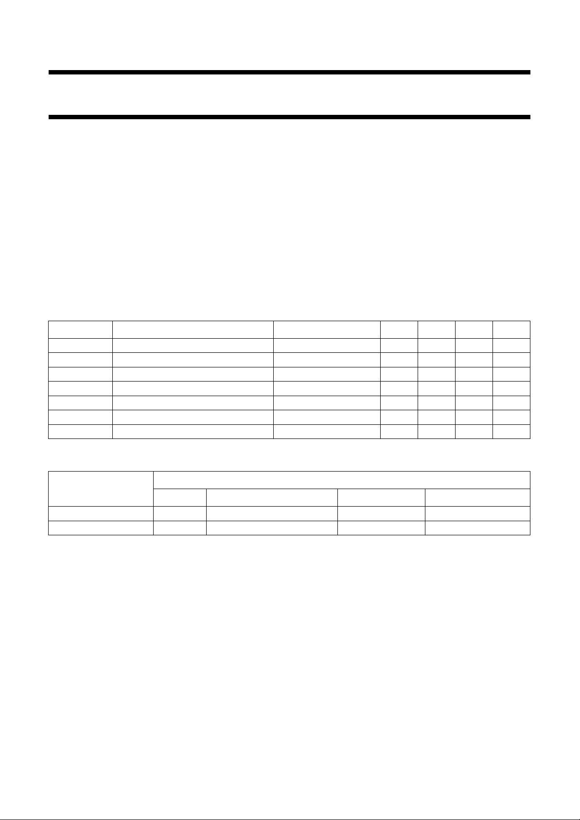
QUICK REFERENCE DATA
SYMBOL PARAMETER CONDITIONS MIN. TYP. MAX. UNIT
V
P
G
v
I
P
positive supply voltage range 3.0 5.0 18 V
internal voltage gain 32.5 33.5 34.5 dB
total quiescent current VP = 5 V; RL = ∞−48mA
SR slew rate − 12 − V/µs
I
I
f
O
bias
co
output current −−0.6 A
input bias current − 100 300 nA
cut-off frequency −3dB − 1.5 − MHz
ORDERING INFORMATION
EXTENDED TYPE
NUMBER
PINS PIN POSITION MATERIAL CODE
PACKAGE
TDA7072A 8 DIL plastic SOT97
TDA7072AT 8 mini-pack plastic SOT96A
Notes
1. SOT97-1; 1996 September 10.
2. SOT96-1; 1996 September 10.
(1)
(2)
July 1994 2
Page 3
Philips Semiconductors Objective specification
Single BTL power driver TDA7072A/AT
V
P
handbook, full pagewidth
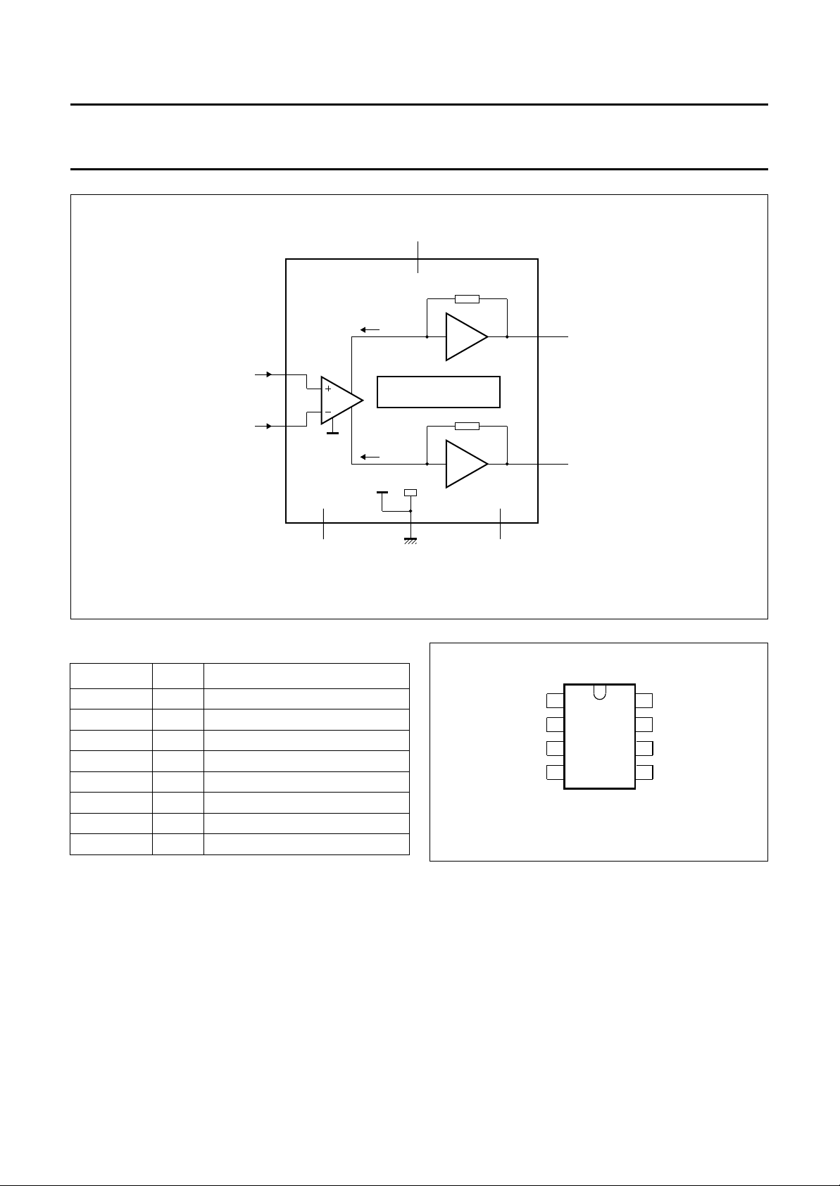
PINNING
positive input
negative input
TDA7072A
TDA7072AT
2
3
n.c.
I + i
SHORT - CIRCUIT AND
THERMAL PROTECTION
I – i
4
6
ground
Fig.1 Block diagram.
1
5
8
7
n.c.
positive output
negative output
MCD377 - 1
SYMBOL PIN DESCRIPTION
V
P
1 positive supply voltage
IN+ 2 positive input
IN− 3 negative input
n.c. 4 not connected
OUT+ 5 positive output
GND 6 ground
n.c. 7 not connected
OUT− 8 negative output
handbook, halfpage
V
IN +
IN –
n.c.
P
1
2
TDA7072A
TDA7072AT
3
4
8
7
6
5
MCD378
Fig.2 Pin configuration.
OUT –
n.c.
GND
OUT +
July 1994 3
Page 4
Philips Semiconductors Objective specification
Single BTL power driver TDA7072A/AT
FUNCTIONAL DESCRIPTION
The TDA7072A/AT are single power driver circuits in a
BTL configuration, intended for use as a power driver for
servo systems with a single supply. They are particular
designed for compact disc players and are capable of
driving focus, tracking, sled functions and spindle motors.
Because of the BTL configuration, the devices can supply
a bi-directional DC current in the load, with only a single
feedback at 33.5 dB and the devices operate in a wide
supply voltage range (3 to 18 V). The devices can supply
a maximum output current of 0.6 A. The outputs can be
short-circuited over the load, to the supply and to ground
at all input conditions. The differential inputs can handle
common mode input voltages from ground level up to
(V
−2.2 V). The devices have a very high slew rate. Due
P
to the large bandwidth, they can handle PWM signals up
to 176 kHz.
supply voltage. The voltage gain is fixed by internal
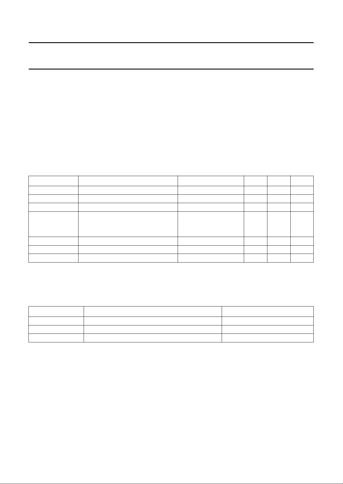
LIMITING VALUES
In accordance with the Absolute Maximum System (IEC 134.
SYMBOL PARAMETER CONDITIONS MIN. MAX. UNIT
V
P
I
ORM
I
OSM
P
tot
positive supply voltage range − 18 V
repetitive peak output current − 1A
non repetitive peak output current − 1.5 A
total power dissipation T
amb
< 25 °C
TDA7072A − 1.25 W
TDA7072AT − 0.54 W
T
stg
T
vj
T
sc
storage temperature range −55 +150 °C
virtual junction temperature − +150 °C
short-circuit time see note − 1hr
Note to the limiting values
The outputs can be short-circuited over the load, to the supply and to ground at all input conditions.
THERMAL RESISTANCE
SYMBOL PARAMETER THERMAL RESISTANCE
R
th j-a
from junction to ambient in free air
TDA7072A 100 K/W
TDA7072AT 155 K/W
Note to the thermal resistance
TDA7072A: V
P
= 0.76 W; T
tot
= 5 V; RL = 8 Ω; The typical voltage swing = 5.8 V and V
P
amb (max)
= 150 − 0.76 × 100 = 74 °C
TDA7072AT: VP = 5 V; RL = 16 typical voltage swing = 5.8 V and V
T
amb (max)
= 150 − 0.38 × 155 = 91 °C
loss
is 2.1 V therefore IO = 0.36 A and
loss
is 2.1 V therefore IO = 0.18 A and P
= 0.38 W;
tot
July 1994 4
Page 5
Philips Semiconductors Objective specification
Single BTL power driver TDA7072A/AT
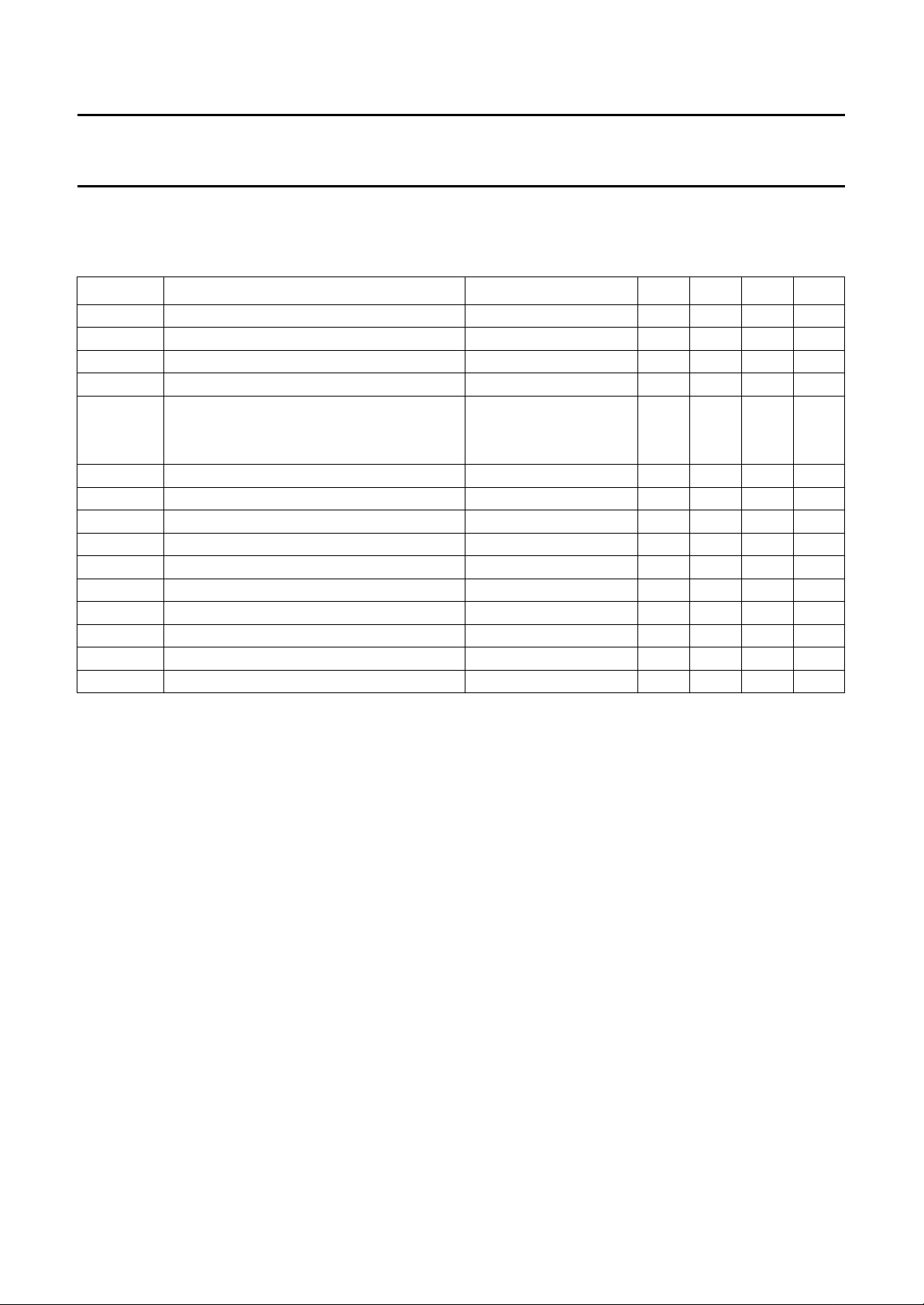
CHARACTERISTICS
= 5 V; f = 1 kHz; T
V
P
TDA7072AT: R
= 16 Ω.
L
SYMBOL PARAMETER CONDITIONS MIN. TYP. MAX. UNIT
V
P
I
ORM
I
P
∆V
OUT
positive supply voltage range 3.0 5.0 18 V
repetitive peak output current −−0.6 A
total quiescent current RL = ∞; note 1 − 48mA
output voltage swing note 2 5.2 5.8 − V
THD total harmonic distortion V
TDA7072A − 0.3 − %
TDA7072AT − 0.1 − %
G
v
V
no(rms)
voltage gain 32.5 33.5 34.5 dB
noise output voltage (RMS value) note 3 − 75 150 µV
B bandwidth −−1.5 MHz
SVRR supply voltage ripple rejection note 4 40 55 − dB
| DC output offset voltage RS = 500 Ω−−100 mV
|∆V
5-8
V
I(CM)
DC common mode voltage range note 5 0 − 2.8 V
CMRR DC common mode rejection ratio note 6 − 100 − dB
Z
I
I
bias
input impedance − 100 − kΩ
input bias current − 100 300 nA
SR slew rate − 12 − V/µs
= 25 °C; unless otherwise specified (see Fig.3>). TDA7072A: RL = 8 Ω;
amb
= 1 V (RMS)
OUT
Notes to the characteristics
1. With a load connected to the outputs the quiescent current will increase, the maximum value of this increase being
equal to the DC output offset voltage divided by R
.
L
2. The output voltage swing is typically limited to 2 x (VP−2.1 V) (see Fig.4).
3. The noise output voltage (RMS value), unweighted (20 Hz to 20 kHz) is measured with RS = 500 Ω.
4. The ripple rejection is measured with RS = 0 Ω and f = 100 Hz to 10 kHz. The ripple voltage of 200 mV (RMS value)
is applied to the positive supply rail.
5. The DC common mode voltage range is limited to (VP−2.2 V).
6. The common mode rejection ratio is measured at V
= 1.4 V, V
ref
= 200 mV and f = 1 kHz.
I(CM)
July 1994 5
Page 6
Philips Semiconductors Objective specification
Single BTL power driver TDA7072A/AT
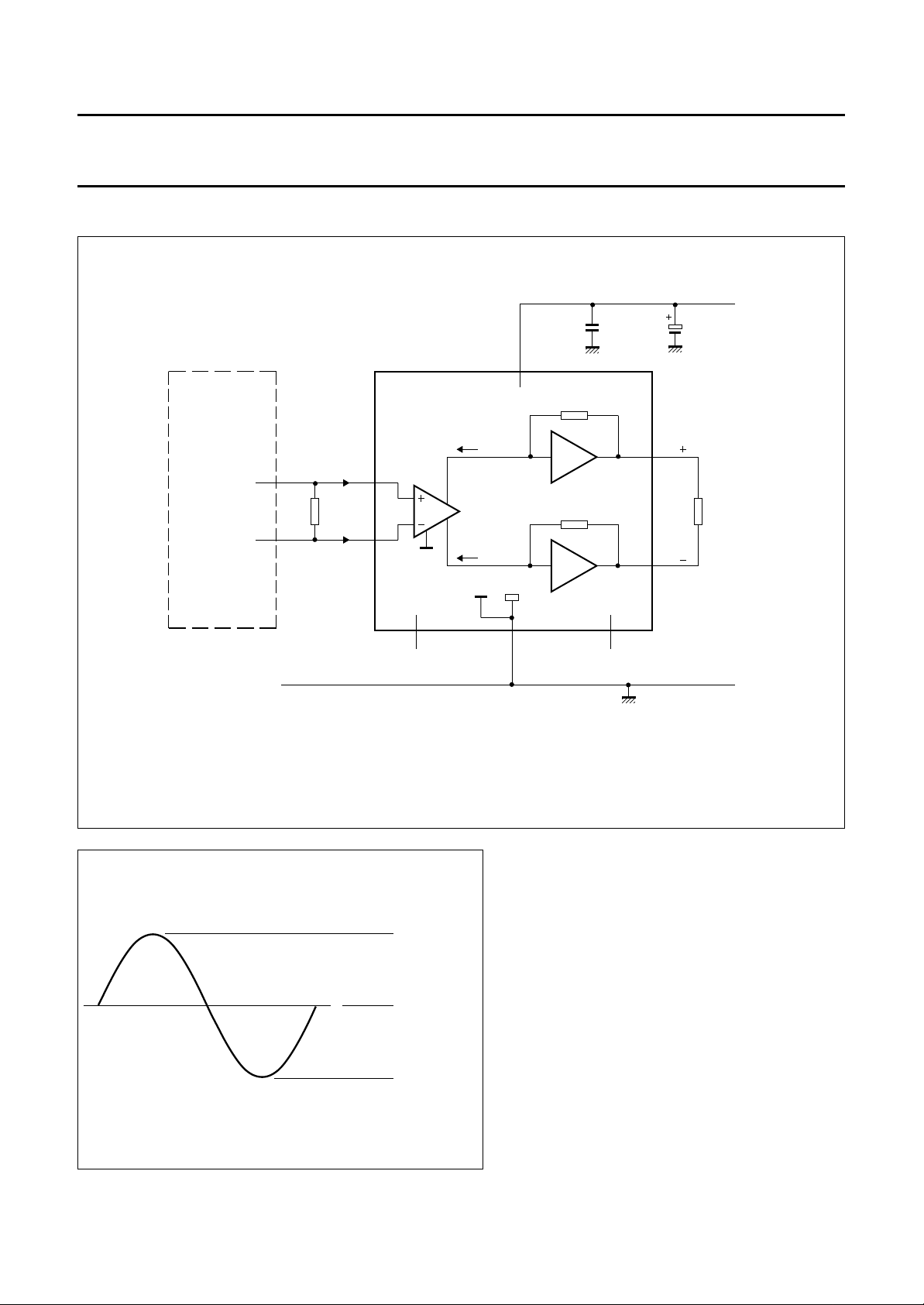
APPLICATION INFORMATION
handbook, full pagewidth
SERVO SYSTEM
driver signal
V
ref
(1)
100 nF
1
220 µF
V = 5 V
P
TDA7072A
TDA7072AT
I + i
2
R
500 Ω
s
3
I – i
4
n.c.
6
7
n.c.
ground
5
(2)
R
L
8
MCD379
(1) This capacitor can be omitted if the 220 µF electrolytic capacitor is connected close to pin 1.
(1) RL can be: focus, tracking, sled function or spindle motor.
Fig.3 Test and application diagram.
+ (V – 2.1) V
P
0 V
– (V – 2.1) V
MCD380
P
Fig.4 Typical output voltage swing over RL.
July 1994 6
Page 7
Philips Semiconductors Objective specification
Single BTL power driver TDA7072A/AT
PACKAGE OUTLINES
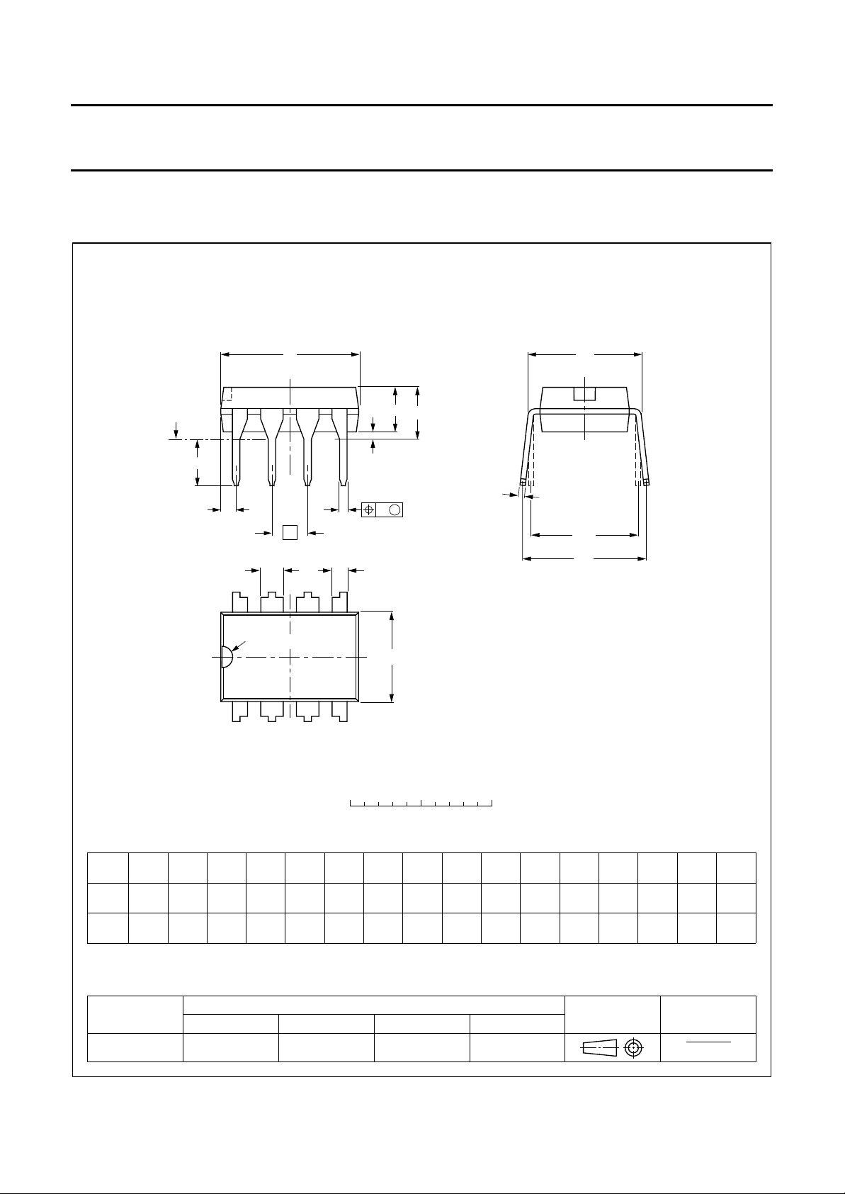
DIP8: plastic dual in-line package; 8 leads (300 mil)
D
seating plane
A
L
Z
e
b
8
pin 1 index
1
w M
b
1
b
2
5
SOT97-1
M
E
A
2
A
c
(e )
1
M
H
E
1
DIMENSIONS (inch dimensions are derived from the original mm dimensions)
A
A
A
UNIT
max.
mm
inches
Note
1. Plastic or metal protrusions of 0.25 mm maximum per side are not included.
OUTLINE
VERSION
SOT97-1
12
min.
max.
050G01 MO-001AN
b
1.73
1.14
0.068
0.045
IEC JEDEC EIAJ
0.021
0.015
b
1
0.53
0.38
4
0 5 10 mm
scale
b
1.07
0.89
0.042
0.035
REFERENCES
cD E e M
2
0.36
0.23
0.014
0.009
0.39
0.36
July 1994 7
(1) (1)
9.8
9.2
6.48
6.20
0.26
0.24
L
e
1
M
3.60
8.25
3.05
7.80
0.14
0.32
0.12
0.31
EUROPEAN
PROJECTION
E
10.0
0.39
0.33
H
8.3
w
max.
0.2542.54 7.62
1.154.2 0.51 3.2
0.010.10 0.30
0.0450.17 0.020 0.13
ISSUE DATE
92-11-17
95-02-04
(1)
Z
Page 8
Philips Semiconductors Objective specification
Single BTL power driver TDA7072A/AT
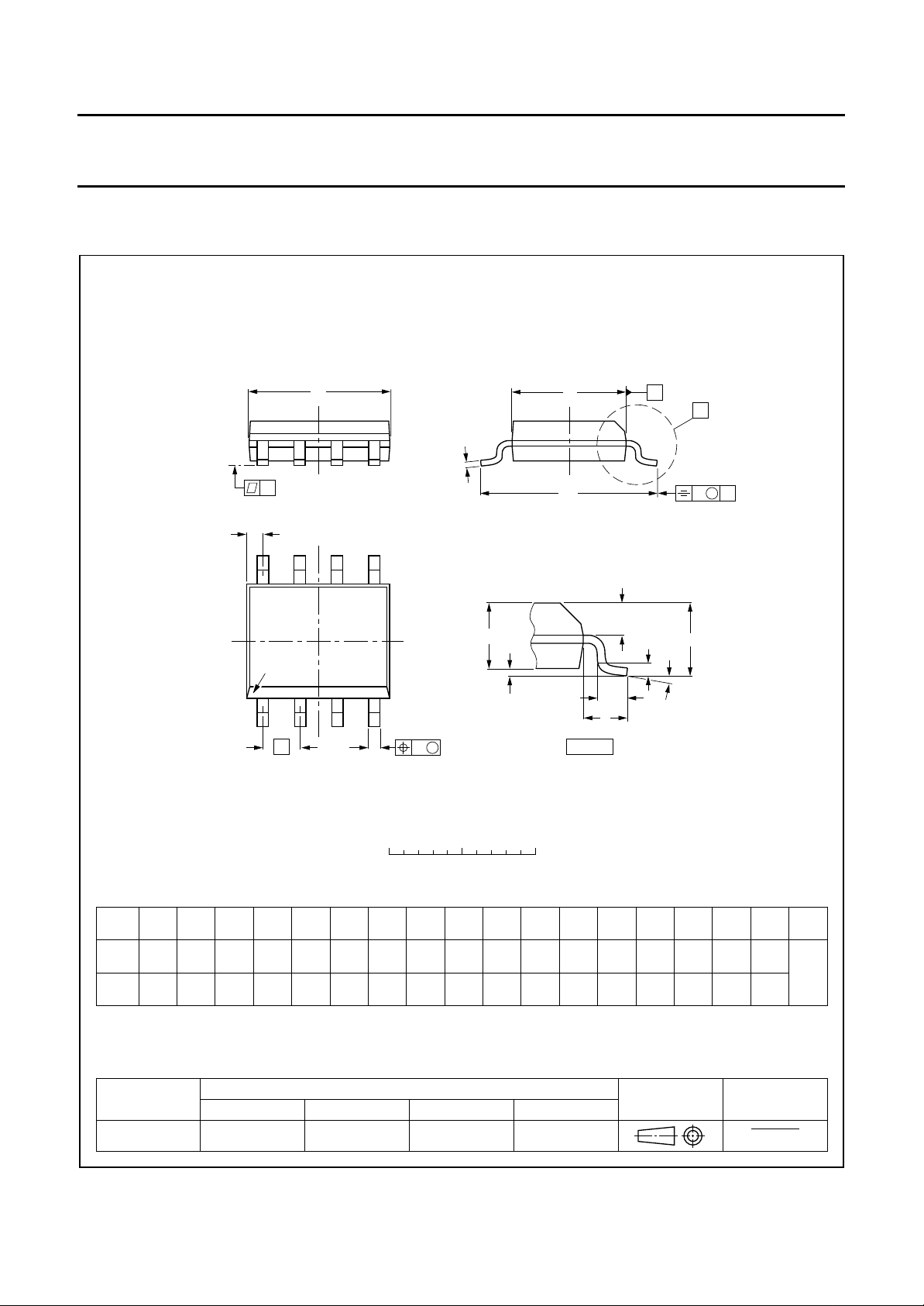
SO8: plastic small outline package; 8 leads; body width 3.9 mm
D
c
y
Z
8
pin 1 index
1
e
5
A
2
A
4
w M
b
p
SOT96-1
E
H
E
1
L
detail X
A
X
v M
A
Q
(A )
L
p
A
3
θ
0 2.5 5 mm
scale
DIMENSIONS (inch dimensions are derived from the original mm dimensions)
mm
OUTLINE
VERSION
SOT96-1
A
max.
1.75
0.069
A1A2A
0.25
1.45
0.10
1.25
0.0098
0.057
0.0039
0.049
IEC JEDEC EIAJ
076E03S MS-012AA
0.25
0.01
b
3
p
0.49
0.25
0.36
0.19
0.019
0.0098
0.014
0.0075
UNIT
inches
Notes
1. Plastic or metal protrusions of 0.15 mm maximum per side are not included.
2. Plastic or metal protrusions of 0.25 mm maximum per side are not included.
(1)E(2)
cD
5.0
4.8
0.20
0.19
REFERENCES
4.0
3.8
0.16
0.15
0.050
July 1994 8
eHELLpQZywv θ
1.27
6.2
5.8
0.24
0.23
1.05
1.0
0.4
0.039
0.016
0.7
0.6
0.028
0.024
0.25 0.10.25
0.010.010.041 0.004
EUROPEAN
PROJECTION
(1)
0.7
0.3
0.028
0.012
ISSUE DATE
92-11-17
95-02-04
o
8
o
0
Page 9

Philips Semiconductors Objective specification
Single BTL power driver TDA7072A/AT
SOLDERING
Introduction
There is no soldering method that is ideal for all IC
packages. Wave soldering is often preferred when
through-hole and surface mounted components are mixed
on one printed-circuit board. However, wave soldering is
not always suitable for surface mounted ICs, or for
printed-circuits with high population densities. In these
situations reflow soldering is often used.
This text gives a very brief insight to a complex technology.
A more in-depth account of soldering ICs can be found in
“IC Package Databook”
our
(order code 9398 652 90011).
DIP
OLDERING BY DIPPING OR BY WA VE
S
The maximum permissible temperature of the solder is
260 °C; solder at this temperature must not be in contact
with the joint for more than 5 seconds. The total contact
time of successive solder waves must not exceed
5 seconds.
The device may be mounted up to the seating plane, but
the temperature of the plastic body must not exceed the
specified maximum storage temperature (T
stg max
). If the
printed-circuit board has been pre-heated, forced cooling
may be necessary immediately after soldering to keep the
temperature within the permissible limit.
R
EPAIRING SOLDERED JOINTS
Apply a low voltage soldering iron (less than 24 V) to the
lead(s) of the package, below the seating plane or not
more than 2 mm above it. If the temperature of the
soldering iron bit is less than 300 °C it may remain in
contact for up to 10 seconds. If the bit temperature is
between 300 and 400 °C, contact may be up to 5 seconds.
SO
REFLOW SOLDERING
Reflow soldering techniques are suitable for all SO
packages.
Several techniques exist for reflowing; for example,
thermal conduction by heated belt. Dwell times vary
between 50 and 300 seconds depending on heating
method. Typical reflow temperatures range from
215 to 250 °C.
Preheating is necessary to dry the paste and evaporate
the binding agent. Preheating duration: 45 minutes at
45 °C.
AVE SOLDERING
W
Wave soldering techniques can be used for all SO
packages if the following conditions are observed:
• A double-wave (a turbulent wave with high upward
pressure followed by a smooth laminar wave) soldering
technique should be used.
• The longitudinal axis of the package footprint must be
parallel to the solder flow.
• The package footprint must incorporate solder thieves at
the downstream end.
During placement and before soldering, the package must
be fixed with a droplet of adhesive. The adhesive can be
applied by screen printing, pin transfer or syringe
dispensing. The package can be soldered after the
adhesive is cured.
Maximum permissible solder temperature is 260 °C, and
maximum duration of package immersion in solder is
10 seconds, if cooled to less than 150 °C within
6 seconds. Typical dwell time is 4 seconds at 250 °C.
A mildly-activated flux will eliminate the need for removal
of corrosive residues in most applications.
EPAIRING SOLDERED JOINTS
R
Fix the component by first soldering two diagonally-
opposite end leads. Use only a low voltage soldering iron
(less than 24 V) applied to the flat part of the lead. Contact
time must be limited to 10 seconds at up to 300 °C. When
using a dedicated tool, all other leads can be soldered in
one operation within 2 to 5 seconds between
270 and 320 °C.
Reflow soldering requires solder paste (a suspension of
fine solder particles, flux and binding agent) to be applied
to the printed-circuit board by screen printing, stencilling or
pressure-syringe dispensing before package placement.
July 1994 9
Page 10

Philips Semiconductors Objective specification
Single BTL power driver TDA7072A/AT
DEFINITIONS
Data sheet status
Objective specification This data sheet contains target or goal specifications for product development.
Preliminary specification This data sheet contains preliminary data; supplementary data may be published later.
Product specification This data sheet contains final product specifications.
Limiting values
Limiting values given are in accordance with the Absolute Maximum Rating System (IEC 134). Stress above one or
more of the limiting values may cause permanent damage to the device. These are stress ratings only and operation
of the device at these or at any other conditions above those given in the Characteristics sections of the specification
is not implied. Exposure to limiting values for extended periods may affect device reliability.
Application information
Where application information is given, it is advisory and does not form part of the specification.
LIFE SUPPORT APPLICATIONS
These products are not designed for use in life support appliances, devices, or systems where malfunction of these
products can reasonably be expected to result in personal injury. Philips customers using or selling these products for
use in such applications do so at their own risk and agree to fully indemnify Philips for any damages resulting from such
improper use or sale.
July 1994 10
 Loading...