

Page 1

INTEGRATED CIRCUITS
DATA SH EET
TDA5149G
12 V Voice Coil Motor (VCM) driver
and spindle motor pre-driver
combination chip
Product specification
File under Integrated Circuits, IC11
1996 May 06
Page 2

Philips Semiconductors Product specification
12 V Voice Coil Motor (VCM) driver and
spindle motor pre-driver combination chip
FEATURES
General features
• Single-chip voice coil motor driver and spindle motor
pre-driver
• Internal voltage reference generator
• Programming of timing parameters via the serial bus
• Control of sleep, brake and disable modes for both the
VCM and spindle via the serial bus
• Temperature monitor circuit
• General purpose uncommitted operational amplifier.
Voice coil motor driver
• On-board full-bridge power DMOS driver with low R
• Class AB linear amplifier with no dead zone
• Adjustable gain and bandwidth
• Retract circuit operating at power-down.
Spindle motor pre-driver
• Designed to drive external N-channel power MOSFETs
for brushless, sensorless DC motors
• Internal or external commutation control
• Digital commutation timing
• Average motor supply current control with Pulse Width
Modulation (PWM)
• Soft switching under PWM control
• Spindle brake after park at power-down.
DSon
APPLICATIONS
• 12 V high-performance hard disk drives.
GENERAL DESCRIPTION
The TDA5149G is a combination of a voice coil motor
driver and a spindle motor pre-driver, capable of operating
12 V high-performance hard disk drives.
The device integrates a spindle pre-driver that drives three
external N-channel power MOSFETs in order to drive a
three-phase brushless, sensorless DC motor in full wave
mode. In the normal mode, commutations are generated
from the internal Back EMF (BEMF) sensing circuitry.
Commutations, however, can also be generated from an
external source, thereby providing the possibility of driving
the motor in the stepper-motor mode.
The VCM driver is a linear transconductance amplifier
capable of handling currents up to 1.65 A. It allows
external adjustment of the gain and compensation.
The TDA5149G also contains two drivers for a latch that
secures the heads in the event of power-down.
To control functions such as park, brake, sleep or disable
and to program the different timing parameters, the
TDA5149G is provided with a three-wire serial port. A high
precision voltage monitor is also included, for both
5 and 12 V power supplies. Finally, the IC contains a
temperature monitor circuit and an uncommitted
operational amplifier connected to VDD, which can be used
freely within the application. The device is contained in a
LQFP64 package with 4 pins connected to the lead frame
for improved heat dissipation.
TDA5149G
QUICK REFERENCE DATA
SYMBOL PARAMETER CONDITIONS MIN. TYP. MAX. UNIT
V
DD
V
DDD
V
DDA1
I
oVCM
R
DSon
ORDERING INFORMATION
TYPE
NUMBER
TDA5149G LQFP64 plastic low profile quad flat package; 64 leads; body 10 × 10 × 1.4 mm SOT314-2
1996 May 06 2
general supply voltage (pin 54) 10.8 12.0 13.2 V
digital supply voltage (pin 55) 4.5 5.0 5.5 V
analog supply voltage (pin 27) 4.5 5.0 5.5 V
voice coil motor output current − − 1.65 A
VCM power DMOS total on-resistance
(including leads and bond wires)
NAME DESCRIPTION VERSION
Tj= 25 °C − − 0.65 Ω
Tj= 125 °C − − 1.1 Ω
PACKAGE
Page 3
Philips Semiconductors Product specification
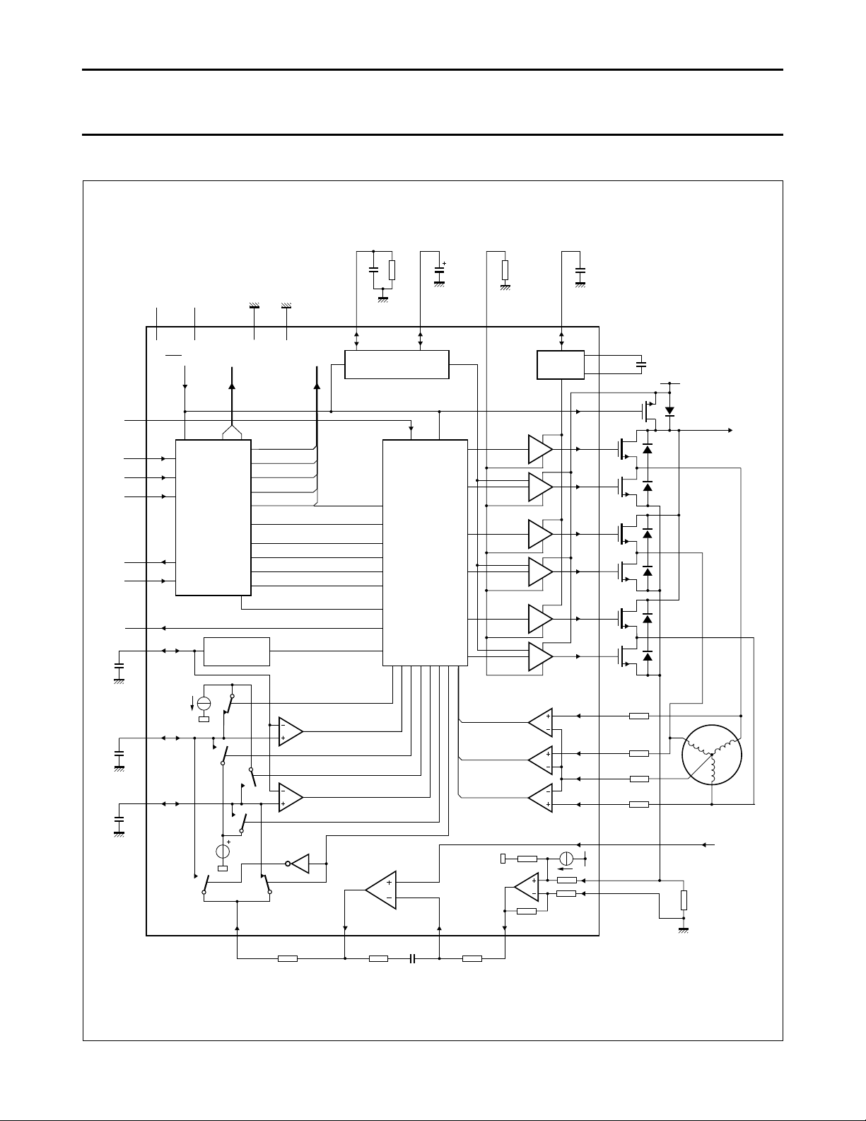
Fig.1 Block diagram of the spindle part.
handbook, full pagewidth
MGE657
SAWTOOTH
OSCILLATOR
SERIAL
PORT
VPARK
VCM_CONT1
VCM_CONT2
VGAINSEL
SLEEP
COMMUT. DELAYS
SBRAKE
SDISABLE
SPINMODE
COMMCLOCK
INIT
TRIGGER
CSS2 dis
SPWM comp 1
SPWM comp 2
CSS2 short
CSS1 dis
CSS1 short
LOOP1 select
CHARGE
PUMP
BRAKE
DELAY
22
CSS1
CSS2
23
STOSC
24
FG
57
SCANTEST
56
SCANOUT
25
SENABLE
61
SDATA
59
SCLOCK
60
CLOCK
58
54
V
DD
45
H0
3
H1
5
L1
6
H2
8
L2
9
H3
11
L3
4
MOT1
7 MOT2
2
MOT0
10
MOT3
19
ISPIN
13
14
SPINSENSEH
SPINSENSEL
63
62
CAPX2
CAPX1
12 V
CLAMP
to the
VCM
MOT1
MOT2
MOT3
3 kΩ
3 kΩ
1 kΩ
3 kΩ
from the
PWM DAC
R
sense
1
CAPY
IDRIVE
12
BRAKEPOWER
BRAKEDELAY
AGND
DGND
64
16
51
47
V
DDA1
V
DDD
55
27
from the
POR circuit
to the
LATCH
to the
VCM
DIGITAL
CONTROL
21
RPOS
20
SICOMP
18
SINTIN
15
SISENS
5×
INTG
COMP
COMP
BEMF comp 1
BEMF comp 2
BEMF comp 3
DRIVER
DRIVER
DRIVER
DRIVER
DRIVER
DRIVER
COMP
COMP
COMP
0.4 V
LACTIVE
LHOLD
TDA5149G
1
2
3
1
2
3
4
5
BLOCK DIAGRAMS
12 V Voice Coil Motor (VCM) driver and
spindle motor pre-driver combination chip
TDA5149G
1996 May 06 3
Page 4

Philips Semiconductors Product specification
Fig.2 Block diagram of the VCM and RESET circuits.
handbook, full pagewidth
MGE656
M
FOLLOWER
FOLLOWER
PREAMP
PREAMP
PARK
CIRCUITRY
SENSE
BUFFER
REFERENCE
CURRENT
GENERATOR
REFERENCE
VOLTAGE
GENERATOR
LATCH
CIRCUITRY
LACTIVE LHOLD
from the
serial port
TEMPERATURE
SENSOR
POWER-
ON RESET
GENERATOR
OPAMP
to the
PARK
circuit
COMP
COMP
+5 V
+12 V
+12 v
from the
serial port
from the
POR circuit
C
comp
R
comp
V
CMIN2
V
CMIN1
R
fb
V
CMSENSOUT
VCM
ref
V
ref(o)
I
ref
POR12
ADJ
POR5
ADJ
VCM_CONT1
VCM_CONT2
AMPIN−
AMPIN+
AMPOUT
CLAMP
PGND1
V
DDV
V
CM+
V
CM−
PGND2
V
CMSENSEL
V
CMSENSEH
latch
LATCHACTIV
LATCHHOLD
TEMPMON
RESETPRESETA
POR
DELAY
26 35 34
37
52
53
42
48
43
44
39
36
32
38
33
31
30
40
41
50
46
49
17
29
28
100 nF
R
8
from the
spindel
27 Ω
100 nF
27 Ω
R
in2
R
in1
VCM
input
VCM
reference
input
TDA5149G
disable
park
brake
V
GAINSEL
V
CMref
R
R
*
20 kΩ
23 kΩ
50 kΩ
10 kΩ
10 kΩ
50 kΩ
−
+
−
+
−
+
+
−
−
+
−
+
+5 V
+12 V
12 V Voice Coil Motor (VCM) driver and
spindle motor pre-driver combination chip
TDA5149G
1996 May 06 4
Page 5

Philips Semiconductors Product specification
12 V Voice Coil Motor (VCM) driver and
spindle motor pre-driver combination chip
PINNING
SYMBOL PIN I/O DESCRIPTION
CAPY 1 I/O charge pump capacitor
MOT0 2 I motor centre tap input
H1 3 O driver output to gate of upper power FET 1
MOT1 4 I back EMF comparator input 1
L1 5 O driver output to gate of lower power FET 1
H2 6 O driver output to gate of upper power FET 2
MOT2 7 I back EMF comparator input 2
L2 8 O driver output to gate of lower power FET 2
H3 9 O driver output to gate of upper power FET 3
MOT3 10 I back EMF comparator input 3
L3 11 O driver output to gate of lower power FET 3
IDRIVE 12 I adjustment for output stage drive current
SPINSENSEH 13 I positive spindle sense amplifier input
SPINSENSEL 14 I negative spindle sense amplifier input
SISENS 15 O spindle sense amplifier output
AGND 16 − general analog ground; note 1
I
ref
SINTIN 18 I negative integrator input
ISPIN 19 I positive integrator input, average current adjustment
SICOMP 20 O integrator output
RPOS 21 I duty cycle modulator input
CSS1 22 I/O soft switching capacitor 1
CSS2 23 I/O soft switching capacitor 2
STOSC 24 I/O sawtooth oscillator capacitor
SCANOUT 25 O test output
POR
DELAY
V
DDA1
POR5
ADJ
POR12
ADJ
AMPIN− 30 I negative input of the uncommitted operational amplifier
AMPIN+ 31 I positive input of the uncommitted operational amplifier
PGND1 32 − power ground 1 for VCM DMOS; note 1
AMPOUT 33 O uncommitted operational amplifier output
RESETP 34 O power-on reset digital output with passive pull-up resistor
RESETA 35 O power-on reset digital output with active pull-up resistor
V
CM−
TEMPMON 37 O temperature monitor output
CLAMP 38 I/O clamp capacitor used for head retraction
V
DDV
V
CMIN2
17 O reference current generator output
26 I/O power-on reset delay capacitor (active LOW)
27 − analog supply voltage 1 (+5 V)
28 O adjustment of POR threshold (for +5 V)
29 O adjustment of POR threshold (for +12 V)
36 O negative output voltage of the VCM power stage
39 − power supply for VCM DMOS driver (+12 V)
40 I switchable VCM control input voltage
TDA5149G
1996 May 06 5
Page 6

Philips Semiconductors Product specification
12 V Voice Coil Motor (VCM) driver and
spindle motor pre-driver combination chip
SYMBOL PIN I/O DESCRIPTION
V
CMIN1
V
CMSENSEH
V
CMSENSEL
V
CM+
H0 45 O gate control of the isolating power FET
VCM
ref
BRAKEPOWER 47 I/O reservoir capacitor for the brake/park circuitry
PGND2 48 − power ground 2 for VCM DMOS; note 1
V
ref(o)
V
CMSENSOUT
BRAKEDELAY 51 I/O powerless brake delay adjustment
LATCHHOLD 52 O latch hold output
LATCHACTIV 53 O latch activate output
V
DD
V
DDD
SCANTEST 56 I test mode input
FG 57 O commutation frequency generator output
CLOCK 58 I clock for digital timing input
SDATA 59 I serial port data input
SCLOCK 60 I serial port clock input
SENABLE 61 I serial port enable input
CAPX2 62 I/O charge pump capacitor input/output
CAPX1 63 I/O charge pump capacitor input/output
DGND 64 − digital ground; note 1
41 I VCM control input voltage
42 I positive VCM sense amplifier input voltage
43 I negative VCM sense amplifier input voltage
44 O positive output voltage of the VCM power stage
46 I reference voltage input for the VCM
49 O reference voltage generator output
50 O VCM sense amplifier output voltage
54 − general supply voltage (+12 V)
55 − digital supply voltage (+5 V)
TDA5149G
Note
1. The 4 ground pins are tied to the lead frame for better heat dissipation.
1996 May 06 6
Page 7

Philips Semiconductors Product specification
Fig.3 Pin configuration.
handbook, full pagewidth
TDA5149G
MGE654
1
2
3
4
5
6
7
8
9
10
11
12
13
14
15
16
48
47
46
45
44
43
42
41
40
39
38
37
36
35
34
33
PGND2
BRAKEPOWER
VCM
ref
H0
V
CM+
V
CMSENSEL
V
CMSENSEH
V
CMIN1
V
CMIN2
V
DDV
CLAMP
TEMPMON
V
CM−
RESETA
RESETP
AMPOUT
CAPY
MOT0
H1
MOT1
L1
H2
MOT2
L2
H3
MOT3
L3
IDRIVE
SPINSENSEH
SPINSENSEL
SISENS
AGDN
17
18
19
20
21
22
23
24
25
26
27
28
29
30
31
32
64
63
62
61
60
59
58
57
56
55
54
53
52
51
50
49
DGND
CAPX1
CAPX2
SENABLE
SCLOCK
SDATA
CLOCK
FG
SCANTEST
V
DDD
V
DD
LATCHACTIV
LATCHHOLD
BRAKEDELAY
V
CMSENSOUT
V
ref(o)
I
ref
SINTIN
ISPIN
SICOMP
RPOS
CSS1
CSS2
STOSC
SCANOUT
POR
DELAY
V
DDA1
POR5
ADJ
POR12
ADJ
AMPIN−
AMPIN+
PGND1
12 V Voice Coil Motor (VCM) driver and
spindle motor pre-driver combination chip
TDA5149G
1996 May 06 7
Page 8

Philips Semiconductors Product specification
12 V Voice Coil Motor (VCM) driver and
spindle motor pre-driver combination chip
FUNCTIONAL DESCRIPTION
Spindle
The spindle section contains both the low and high side
pre-drivers for a three phase DC brushless motor.
The digital commutation control, using the timing
information provided via the serial port, is responsible for
the proper switch-on and switch-off of the external power
FETs. It is also responsible for selecting the correct BEMF
comparator.
For optimum power efficiency, a continuous PWM method
is used to control the average current from the power
supply to the motor coils. This PWM mode, by controlling
the average power supply current, produces a lower
torque ripple and thus lower audible noise. In order to
reduce further acoustic noise the TDA5149G is provided
with a soft switching circuit to turn-on and turn-off linearly
the switching current under PWM control. The switching
transition time is controlled by the digital commutation
circuit and is fixed to 50% of the time between two
zero-crossings, i.e. 30° of the electrical revolution.
Soft switching is achieved by activating, during
commutation, a free-running duty-cycle modulator
controlled by a linearly decreasing voltage across a
capacitor. This will reduce the current smoothly in the
off-going leg to zero. In conjunction with this additional
PWM open loop, the average current control regulates the
sum of the current in the off-going and on-going leg.
This method requires two PWM control loops; one to
control the average current (main loop) and one to control
the current in the off-going leg. The swapping of the two
loops is realized with a pair of analog switches that are
sequentially switched by the digital commutation circuitry.
The PWM control also causes PWM pulses on the back
EMF. These pulses disturb correct sensing of the back
EMF for the zero-crossing detection. Consequently,
edge-triggered latches are inserted behind the back EMF
comparators, thus ensuring reliable back EMF sensing.
In the SPINMODE, programmable via the serial bus, the
user can feed their own commutation pulses to the
pre-drivers and control the motor in the stepper-motor
mode. The commutation pulses are applied to the
TDA5149G via the serial bus by setting the COMMCLK bit
successively to logic 1 and logic 0.
TDA5149G
The different control modes of the TDA5149G can be
commanded via the serial bus. These modes are as
follows:
• Sleep mode: all analog circuits, except the power supply
monitor, are switched off to reduce the power
consumption of both the 12 and 5 V supplies.
• Disable mode: the output voltage of all pre-drivers is
LOW thus the external power MOSFETs are not
conducting.
• Brake mode: all low side pre-drivers are turned on
(output voltage HIGH) thus switching on the low-side
power MOSFETs. In this way the back EMF voltage of
the motor is short-circuited to ground.
Voice coil motor
The VCM is a linear, symmetrical, class AB, H-bridge type
power amplifier with all power devices on-chip. The driver
is a transconductance amplifier that controls the output
currents up to 1.65 A. The driver is constructed in a
master-slave configuration with the zero current level
internally adjusted in such a way that it corresponds to the
middle of the output swing. Moreover, the gain of the slave
has been made greater than 1 in order to ensure full
saturation of the driver output VCM+.
The gain of the closed loop is programmable, using the
V
GAINSEL
bus. A sense resistor (Rs) allows the measurement of the
VCM current. The voltage across this resistor is connected
to an accurate sense amplifier with a typical gain of 5.
The output of the sense amplifier (V
to the input of the VCM amplifier. Because of the symmetry
of the circuit, the compensation network can be connected
between the VCM1 input and the VCM− output.
Control modes such as VCM-BRAKE, VCM-DISABLE and
VCM-PARK can be controlled via the serial bus.
Latch drivers
The TDA5149G provides the possibility of driving an
external latch to secure the VCM heads. There are two
modes; the activate mode (LACTIVE) and the hold mode
(LHOLD). The hold mode is used to preserve power.
Both modes are controlled via the serial bus. The drivers
are switched off during the SLEEP mode or in the event of
a power-down.
bit. This bit can be programmed via the serial
CMSENSOUT
) is fed back
1996 May 06 8
Page 9

Philips Semiconductors Product specification
12 V Voice Coil Motor (VCM) driver and
spindle motor pre-driver combination chip
Power-on/power-off reset
The power-on reset circuitry monitors the analog, digital
and general supplies. The voltage thresholds have been
set internally for both supplies, i.e. 4.4 V for V
V
, and 10.5 V for VDD. External adjustment and
DDD
filtering, to suppress supply spikes, has been made
possible through the pins POR5
and POR12
ADJ
When either of the supplies falls below their threshold
levels, the reset circuit provides two active LOW output
signals. The RESETA signal is a full CMOS output and the
RESETP signal has an active pull-down MOS transistor
with a passive pull-up resistance of 10 kΩ. The latter can
be used for emulation purposes. Both signals remain LOW
until the supply voltages are again above the threshold
level, delayed by a time constant period that is determined
by the value of the capacitor connected to pin POR
A park sequence is initiated on a reset fault. This includes
disabling the actuator latch drivers and starting a delayed
spindle brake operation by switching on the low side
pre-drivers simultaneously. This brake delay is determined
by an external RC combination connected to
BRAKEDELAY. Actuator PARK and spindle BRAKE can
also be controlled via the serial port.
At power-up, the two reset output signals (RESETA and
RESETP) will remain LOW as long as either supply
voltage is below the specified threshold plus the hysteresis
voltage. Once the supply voltages are above their specific
trip levels, the two reset signals become HIGH after the
power-on reset delay (POR
). This delay time is
DELAY
determined by the value of the capacitor connected to the
POR
DELAY
pin.
DDA
ADJ
and
.
DELAY
.
TDA5149G
To ensure that the stored energy in the clamp capacitor is
only used for the park operation, the CLAMP input must be
isolated from the power supply. This can be achieved by
using a Schottky diode or a reverse connected N-channel
power FET (see Fig.1). The TDA5149G provides an
output H0 to control this power FET.
At power-down the brake delay circuit is also enabled.
The brake delay circuit is supplied by the energy stored in
the capacitor (charged during normal operation from VDD)
that is connected to the BRAKEPOWER pin. Both the
BRAKEDELAY and BRAKEPOWER pins are then isolated
from the 12 V supply voltage. When the voltage on the
BRAKEDELAY pin reaches a value of 1.6 V (typ.), the
low-side external power FETs are turned on to brake the
spindle motor. The BRAKEPOWER capacitor then
supplies the current to keep the power FETs conducting.
This means that the voltage on this capacitor decreases
with time.
Serial port
The serial port is used to modify the various operational
modes of the TDA5149G and to adjust the timing
parameters to ensure the proper commutation sequence
of the spindle motor. It is a synchronous, slave only,
three-wire communication port with data (SDATA), clock
(SCLOCK) and enable (SENABLE) inputs.
The serial port requires the data to be sent in bytes, the
LSB (data 0) to be sent first and the MSB (address 2) last.
The three most significant bits (MSBs) determine the
register address, the remaining five bits represent the
data, which means up to 8 registers can be independently
addressed.
Powerless park/brake
As with the normal retract procedure, an actuator park
sequence is initiated whenever a power-down situation
occurs. The power-on/power-off reset circuit generates the
two active LOW reset signals and also activates the VCM
park circuit. The VCM park circuit provides a voltage,
retrieved from the rectified back EMF voltage of the
running-out spindle, of 1.2 V (typ.) to the VCM pin.
The voltage at pin VCM+ is 0 V. This voltage is supplied by
the capacitor C
that is connected to the CLAMP pin.
CLAMP
This capacitor smooths the rectified back EMF and stores
the electrical energy generated by the motor.
1996 May 06 9
When SENABLE is LOW, the serial port is disabled and
the IC is not affected by any change both on SDATA and
SCLOCK. When SENABLE is HIGH the data is written
serially to the shift register on the rising edge of SCLOCK.
When SENABLE goes LOW the shifting sequence is
stopped and the last 8 bits that are clocked in are latched
into the appropriate control register. Therefore, the
transmission of two consecutive bytes requires that
SENABLE is LOW for at least a duration of ‘t’
(see Chapter “Characteristics”).
Page 10

Philips Semiconductors Product specification
Fig.4 Power-on/power-off reset timing.
handbook, full pagewidth
MBH021
V
CC
POR
0.8 V
V
hys
threshold
t
t
t
C
t
C
Fig.5 Serial port signal timing
handbook, full pagewidth
MGE655
t
pm
t
h1
t
su1
t
su1
t
su2
t
h2
t
su2
t
h2
SCLOCK
SENABLE
SDATA
12 V Voice Coil Motor (VCM) driver and
spindle motor pre-driver combination chip
TDA5149G
1996 May 06 10
Page 11

Philips Semiconductors Product specification
12 V Voice Coil Motor (VCM) driver and
TDA5149G
spindle motor pre-driver combination chip
Table 1 Serial port registers
REGISTER
ADDRESSED
Reg # 0 INIT COMMCLCK SPINMODE SDISABLE SBRAKE
Reg # 1 not used HARD_SW LHOLD LACTIVATE SLEEP
Reg # 2 not used not used VGAINSEL VCM_CTRL_1 VCM_CTRL_0
Reg # 3 not used not used PRESCALER_2 PRESCALER_1 PRESCALER_0
Reg # 4 STARTUP_4 STARTUP_3 STARTUP_2 STARTUP_1 STARTUP_0
Reg # 5 WATCHDOG_4 WATCHDOG_3 WATCHDOG_2 WATCHDOG_1 WATCHDOG_0
Reg # 6 not used not used COMDELIM_2 COMDELIM_1 COMDELIM_0
Reg # 7 BLANK_4 BLANK_3 BLANK_2 BLANK_1 BLANK_0
Table 2 REG # 0: address 000; DATA = | INIT | COMMCLK | SPINMODE | SDISABLE | SBRAKE |
DATA BIT
INIT 1 initializes the three bits commutation shift register in state 1 (see Table 13)
COMMCLK 0 commutation clock in stepper mode (one commutation every LOW-to-HIGH transition)
SPINMODE 0 stepper/BEMF detection mode selection. SPINMODE = 1 means stepper motor mode
SDISABLE 1 logic 1 sets the pre-drivers outputs LOW so that the spindle motor coils are in the
SBRAKE 0 logic 1 sets the lower pre-driver outputs HIGH and the upper pre-driver outputs LOW
DATA4 DATA3 DATA2 DATA1 DATA0
RESET
STATE
in hard-switching configuration
high-impedance state
so that the spindle motor coils are shorted to ground
DESCRIPTION
Table 3 REG # 1: address 001; | not used | HARD_SW | LHOLD | LACTIVE | SLEEP |
DATA BIT
HARD_SW 0 logic 1 disables the soft switching circuitry, which means PWM is applied on the lower
LHOLD 0 logic 1 turns on the hold current supplied by V
LACTIVE 0 logic 1 turns on the activate current supplied by VDD through the latch
SLEEP 0 logic 1 disables spindle, VCM and latch driver outputs. The whole analog circuitry is
Table 4 REG # 2: address 010; | not used | not used | VGAINSEL | VCM_CTRL_1 | VCM_CTRL_0 |
DATA BIT
VGAINSEL 1 logic 1 turns on the switch between V
VCM_CTRL_1 1 see Table 5
VCM_CTRL_0 1 see Table 5
RESET
STATE
RESET
STATE
DESCRIPTION
FETs only.This mode is also forced in stepper motor mode.
through the latch. It is ignored if
DDD
LACTIVE = 1
turned off except the reference bandgap and the voltage monitors. The uncommitted
operational amplifier is also cut off.
DESCRIPTION
CMIN1
transconductance of the VCM closed loop
and V
, resulting in a higher gain for the
CMIN2
1996 May 06 11
Page 12

Philips Semiconductors Product specification
12 V Voice Coil Motor (VCM) driver and
TDA5149G
spindle motor pre-driver combination chip
Table 5 Operating conditions for VCM_CTRL_1 and VCM_CTRL_0
VCM_CTRL_1 VCM_CTRL_0 MODE
0 0 VCM operating
0 1 VCM brake
1 0 VCM park
1 1 VCM disable
Table 6 REG # 3: address 011; | not used | not used | PRESCALER_REG [2 to 0]
DATA BIT
PRESCALER_2 0 sets the division factor that is applied to the external clock (pin 58) in order to
PRESCALER_1 1
PRESCALER_0 0
Note
1. CLOCK (pin 58) must be valid before the end of the POR delay.
RESET
STATE
DESCRIPTION
obtain the appropriate internal clock frequency for the proper determination of the
commutation delays. The prescaling factors can be obtained as shown in Table 7
(1)
Table 7 Prescaler factors
PRESCALER_REG FREQUENCY (MHz)
0 0 0 1
0 0 1 2
0 1 0 4
0 1 1 8
1 0 0 16
1 0 1 32
1 1 0 64
1 1 1 128
Note
1. Internal clock frequency is equal to external clock frequency divided by prescaler ratio.
Table 8 REG # 4: address 100; | STARTUP_REG[4 to 0] |
DATA BIT
STARTUP_4 0
STARTUP_3 0
STARTUP_2 0
STARTUP_1 0
STARTUP_0 0
RESET
STATE
DESCRIPTION
The start-up timer instigates the spin-up in the absence of the back EMF zero
crossings. If the rotational speed is high enough, the commutations are
sequenced regardless of the start-up counter. But if no BEMF zero crossing
occurs, which is the case if the motor is stationary or rotating very slowly, the
start-up timer reaches its terminal count given by the STARTUP_REG, thereby
causing the next commutation. If t
STARTUP delay = [(({0 to 31} × 32) + 2) × 511) + 2] × t
is the period of the internal clock then;
IC
(1)
IC
1996 May 06 12
Page 13

Philips Semiconductors Product specification
WATCHDOG delay 0 to 31{ } 64×( ) 1+[ ] tIC×=
{ } 4×( ) 1+[ ] tIC×=
12 V Voice Coil Motor (VCM) driver and
TDA5149G
spindle motor pre-driver combination chip
Table 9 REG # 4: address 101; | WATCHDOG_REG[4 to 0] |
DATA BIT
WATCHDOG_4 0
WATCHDOG_3 0
WATCHDOG_2 0
WATCHDOG_1 0
WATCHDOG_0 0
Table 10 REG # 6: address 110; | not used | not used | COMDELIM_REG[2 to 0] |
DATA BIT
COMDELIM_2 0 Defines the maximum commutation delay limit by setting the saturation value of the
COMDELIM_1 0
COMDELIM_0 0
Table 11 Commutation delay limit
RESET
STATE
RESET
STATE
DESCRIPTION
The watchdog timer checks for correct back EMF polarity, which indicates correct
rotation of the motor
DESCRIPTION
zero crossing counter. tIC represents the period of the internal clock. Table 11
shows the delays which can be obtained.
COMDELIM_REG COUNTER SATURATION VALUE MAXIMUM COMMUTATION DELAY
111 2047 tIC× 1023
110; note 1 1535 tIC× 767
101 1023 tIC× 511
100; note 1 767 tIC× 383
011 511 tIC× 255
010; note 1 383 tIC× 191
001 255 tIC× 127
000; note 1 191 tIC× 95
Note
1. Even COMDELIM _REG values must be avoided.
Table 12 REG # 7: address 111; | BLANK_REG[4 to 0] |
DATA BIT
BLANK_4 0
BLANK_3 0
BLANK_2 0
BLANK_1 0
BLANK_0 0
RESET
STATE
In the hard switching mode, the blank delay inhibits the back EMF comparator
outputs just at the moment the MOT outputs are commutating, until they have been
stabilized again. To avoid false zero-crossing detection, the blank delay operates in
the same way at the end of the fly-back pulse (hard-switching mode), or at the end
of the soft-switching interval (soft-switching mode).
BLANK delay 0 to 31
DESCRIPTION
1996 May 06 13
Page 14

Philips Semiconductors Product specification
12 V Voice Coil Motor (VCM) driver and
TDA5149G
spindle motor pre-driver combination chip
Table 13 Configuration of the six commutation states in hard-switching mode
STATE SHIFT REGISTER H1
(3)
1
111 ON − − − PWM −
(1)
2 011 ON − − − − PWM
3 001 − ON − − − PWM
4 000 − ON − PWM − −
5 100 − − ON PWM − −
6 110 − − ON − PWM −
Note
1. H1, H2 and H3 are the upper power FETs connected to MOT1, MOT2 and MOT3 respectively.
2. L1, L2 and L3 are the lower power FETs connected to MOT1, MOT2 and MOT3 respectively.
3. INIT = 1 means ‘state 1’ situation with PWM stuck in OFF on L2.
LIMITING VALUES
In accordance with the Absolute Maximum Rating System (IEC 134).
SYMBOL PARAMETER CONDITIONS MIN. MAX. UNIT
V
V
V
V
V
DD
DDD
DDA
DDV
CM+
general supply voltage indefinite time period −0.3 +13.5 V
digital supply voltage indefinite time period −0.3 +6.0 V
analog supply voltage indefinite time period −0.3 +6.0 V
supply for VCM DMOS driver indefinite time period −0.3 +13.5 V
output voltage of the VCM power
stage
V
CM−
output voltage of the VCM power
stage
I
CM+
output current of the VCM power
current peak <0.5 s − 2.5 A
stage
ICM− output current of the VCM power
current peak <0.5 s − 2.5 A
stage
V
MOT
BEMF comparator input voltage
(pins 4, 7 and 10)
V
T
T
n
stg
j(max)
input voltages on other pins −0.3 − V
IC storage temperature −55 +125 °C
maximum junction temperature − 150 °C
H2
(1)
H3
(1)
L1
(2)
−0.3 +15 V
−0.3 +7.0 V
−0.3 +7.0 V
−0.3 +15 V
−0.7 +15 V
−0.7 +15 V
−0.7 − V
L2
(2)
L3
(2)
1996 May 06 14
Page 15

Philips Semiconductors Product specification
12 V Voice Coil Motor (VCM) driver and
TDA5149G
spindle motor pre-driver combination chip
HANDLING
Inputs and outputs are protected against electrostatic discharge in normal handling. However, to be totally safe, it is
desirable to take normal precautions appropriate to handling MOS devices.
ESD according to MIL STD 883C - method 3015 (HBM 1500 Ω, 100 pF) 3 pulses positive and 3 pulses negative on each
pin versus ground - Class 1: 0 to 1999 V.
THERMAL CHARACTERISTICS
SYMBOL PARAMETER
R
th j-a
thermal resistance from junction to ambient in free air 54 K/W
Note
1. This is obtained in a standard PCB: standard PCB size: 100 mm × 75 mm × 1.6 mm; material = glass epoxy FR4,
single copper layer. With dedicated PCB tailored to heat dissipation, the thermal resistance could be as low as
40 K/W.
OPERATING CHARACTERISTICS
SYMBOL PARAMETER CONDITIONS MIN. TYP. MAX. UNIT
(1)
VALUE UNIT
Temperature
T
amb
operating ambient temperature −5 − +70 °C
Supplies: pins 27, 55, 54 and 39
V
V
I
DD
I
DDA
V
DDA
DDD
DDV
analog supply voltage 4.5 5.0 5.5 V
digital supply voltage 4.5 5.0 5.5 V
general supply voltage 10.8 12.0 13.2 V
analog supply current normal mode − 5.5 7.5 mA
supply voltage for VCM DMOS
driver
VCM reference voltage: pin 46 (VCM
VCM
ref
reference voltage input level 1.9 − 4.0 V
Charge pump: pin 1 (CAPY)
C
C
CAPX
CAPY
charge pump capacitor between CAPX1 and CAPX2 6.8 10 13 nF
charge pump capacitor between CAPY and ground 16 22 30 nF
CLAMP: pin 38
C
CLAMP
clamp capacitance between CLAMP and ground − 47 − µF
BRAKEPOWER: pin 47
C
BP
brakepower capacitance note 1 − 47 − µF
Sense resistors
R
SSENS
R
VSENS
spindle sense resistor 0.15 − − Ω
VCM sense resistor 0.15 − − Ω
ref
10.8 12.0 13.2 V
)
1996 May 06 15
Page 16

Philips Semiconductors Product specification
12 V Voice Coil Motor (VCM) driver and
TDA5149G
spindle motor pre-driver combination chip
SYMBOL PARAMETER CONDITIONS MIN. TYP. MAX. UNIT
Spindle pre-drivers: pin 12 (IDRIVE)
R
IDRIVE
Reference current: pin 17 (I
R
Iref
Sawtooth oscillator: pin 24 (STOSC)
C
SO
Power-on reset: pin 26 (POR
C
PORDELAY
Digital inputs for the serial port: pins 58 to 61 (CLOCK, SDATA, SCLOCK and SENABLE)
V
IH
V
IL
Notes
1. To guarantee a powerless brake duration of at least 10 s. A low leakage capacitor must be used (<0.1 µA).
2. For a frequency range of 25 to 100 kHz. C
3. For a RESETA/RESETP pulse duration of approximately 100 ms.
resistance for pre-driver current
32 − 470 kΩ
adjustment
)
ref
resistance for reference current
47 − 470 kΩ
adjustment
sawtooth oscillator capacitance note 2 150 − 700 pF
)
DELAY
POR
capacitance note 3 − 100 − nF
DELAY
HIGH level input voltage 2.4 − − V
LOW level input voltage − − 0.8 V
STOSC
= 0.775 (I
ref/fPWM
).
CHARACTERISTICS
VDD= 12 V; V
DDA
= V
DDD
= 5 V; T
= 25 °C; unless otherwise specified.
amb
SYMBOL PARAMETER CONDITIONS MIN. TYP. MAX. UNIT
Supplies: pins 27, 55 and 54
I
DDA
analog supply current normal mode − 5.5 7.5 mA
sleep mode − 1.6 2.0 mA
I
DDD
digital supply current normal mode − 5.5 7.5 mA
sleep mode − 1.6 2.0 mA
I
DD
general supply current normal mode − 12 17 mA
sleep mode − 2.9 4.0 mA
VOLTAGE REFERENCE: PIN 49 (V
V
ref(o)
reference voltage generator
ref(o)
)
I
= ±1 mA 2.47 2.57 2.67 V
ref(o)
output
CURRENT REFERENCE: PIN 17 (I
I
ref(o)
reference current generator
ref(o)
)
R
= 120 kΩ; note 1 20.6 21.4 22.2 µA
ref
output
TEMPERATURE MONITOR: PIN 37 (TEMPMON)
V
OLT
output voltage at LOW
Tj= 25 °C 2.15 2.17 2.19 V
temperature
V
OHT
output voltage at HIGH
Tj= 150 °C; note 2 3.03 3.055 3.08 V
temperature
1996 May 06 16
Page 17

Philips Semiconductors Product specification
12 V Voice Coil Motor (VCM) driver and
TDA5149G
spindle motor pre-driver combination chip
SYMBOL PARAMETER CONDITIONS MIN. TYP. MAX. UNIT
VCM REFERENCE: PIN 46 (VCM
I
i
input current V
Spindle: pre-drivers
HARGE PUMP: PIN 1 (CAPY)
C
V
CP
V
ripple(p-p)
charge pump DC voltage I
voltage ripple
(peak-to-peak value)
BACK EMF COMPARATORS: PINS 2, 4, 7 AND 10 (MOT0, MOT1, MOT2 AND MOT3)
V
iCM
I
bias
V
SWhys
∆V
CSW
common mode input voltage note 4 −0.7 − VDD+ 0.7 V
input bias current MOT0 −10 − 0 µA
switching level for hysteresis for negative transition
variation in comparator
switching levels for one IC
V
i(hys)
input voltage hysteresis − 0.5 − mV
SPINDLE LOWER PRE-DRIVERS: PINS 5, 8 AND 11 (L1, L2 AND L3)
V
OH
I
source
I
sink
HIGH level output voltage IOH= −0.5 mA 7.2 8.0 8.8 V
output source current R
output sink current 1.2 1.6 2.0 mA
SR slew rate R
SPINDLE UPPER PRE-DRIVERS: PINS 3, 6 AND 9 (H1, H2 AND H3)
V
OH
I
source
I
sink
HIGH level output voltage IOH= −0.5 mA 18.0 18.8 19.6 V
output source current R
output sink current 1.3 1.75 2.2 mA
SR slew rate R
H0: PIN 45
V
o
output voltage normal condition 18.3 18.8 20 V
OUTPUT CURRENT ADJUSTMENT: PIN 12 (IDRIVE)
I
refSP
spindle pre-driver reference
current
ref
)
= 2 V; note 3 −250 − +60 µA
VCMref
< 1 mA 18.5 19.3 19.8 V
CAPY
I
= 1 mA − − 0.8 V
CAPY
−13 − −7 mV
with respect to MOT0
for positive transition
7 − 13 mV
with respect to MOT0
−4.2 − +4.2 mV
= 120 kΩ; note 5 −0.9 −0.7 −0.5 mA
IDRIVE
= 120 kΩ; note 6 − 10 − V/µs
IDRIVE
= 120 kΩ; note 7 −1.3 −1.0 −0.7 mA
IDRIVE
= 120 kΩ; note 6 − 10 − V/µs
IDRIVE
R
= 120 kΩ; note 7 20.6 21.4 22.2 µA
IDRIVE
Spindle: PWM
SPINDLE SENSE AMPLIFIER: PINS 13 AND 14 (SPINSENSEH AND SPINSENSEL)
∆V
i
I
sense+
differential input voltage 0 − 1.84 V
positive input sense current −60 −51 −42 µA
1996 May 06 17
Page 18

Philips Semiconductors Product specification
12 V Voice Coil Motor (VCM) driver and
TDA5149G
spindle motor pre-driver combination chip
SYMBOL PARAMETER CONDITIONS MIN. TYP. MAX. UNIT
SISENS: PIN 15
∆V
o
V
o
G
S
f
UG
SPINDLE CURRENT LOOP FILTER AMPLIFIER: PINS 18 AND 19 (SINTIN AND ISPIN)
V
iCM
V
i(os)
I
i
SICOMP: PIN 20
V
OL
V
OH
SR slew rate 0.5 0.9 1.5 V/µs
f
UG
SPINDLE PWM COMPARATORS: PINS 22 AND 23 (CSS1 AND CSS2)
V
dc
I
sink(d)
I
sink(s)
ANALOG SWITCHES: PIN 21 (RPOS)
R
Son
R
Soff
SAWTOOTH OSCILLATOR: PIN 24 (STOSC)
V
SUL
V
SLL
I
source
I
sink
Voice coil motor driver
output voltage shift 1.38 1.43 1.48 V
output voltage level 1.37 − VDD− 1.2 V
spindle sense amplifier gain 4.85 5.0 5.15 V/V
unity gain bandwidth 1 − − MHz
common mode input voltage 1.3 − 3.2 V
input offset voltage −3.0 − +3.0 mV
input current −1 − 0 µA
LOW level output voltage IOL= 1 mA − − 0.5 V
HIGH level output voltage IOH= −0.6 mA 3.5 − − V
unity gain bandwidth 1 − − MHz
discharge clamp voltage I
sink current for normal CSS1 and
= 0.5 mA − − 0.45 V
CSS1,2
20.2 21.0 21.8 µA
CSS2 discharge;
R
= 120 kΩ
Iref
sink current for CSS1 and CSS2
1 − − mA
short
switch-on resistance 150 250 400 Ω
switch-off resistance 10 − − MΩ
voltage swing upper limit 2.9 3.0 3.1 V
voltage swing lower limit static test 0.53 0.55 0.57 V
source current note 8 −44.4 −42.8 −41.2 µA
sink current note 9 500 800 1100 µA
VCM PREAMPLIFIERS: PINS 41 AND 40 (V
I
V
f
G
G
i
i(os)
UG
RSon
RSoff
input current −10 − +10 µA
input offset voltage −6 − +6 mV
unity gain bandwidth − 3 − MHz
gain switch-on resistance VGAINSEL = 1 − − 60 Ω
gain switch-off resistance VGAINSEL = 0 10 − − MΩ
CMIN1
AND V
CMIN2
)
1996 May 06 18
Page 19

Philips Semiconductors Product specification
12 V Voice Coil Motor (VCM) driver and
TDA5149G
spindle motor pre-driver combination chip
SYMBOL PARAMETER CONDITIONS MIN. TYP. MAX. UNIT
VCM DRIVER AMPLIFIERS: PINS 44 AND 36 (V
t
COD
G
V
vSD
OD
cross-over switch time − 2 5 µs
slave driver voltage gain 1.12 1.15 1.18 V/V
output drop voltage
including bond wires and
leads
t
RFS
recovery time from saturation − − 100 µs
SR output slew rate 1.4 2.0 − V/µs
f
UG
V
park
VCM
SENSE AMPLIFIER: PINS 43 AND 42 (V
V
I
I
I
V
CMSENSOUT
V
OSL
unity gain bandwidth 1.5 3 − MHz
park voltage over full temperature
input voltage range −0.7 − VDD+ 0.7 V
input current common mode from
: PIN 50
LOW level output saturation
voltage
V
OSH
HIGH level output saturation
voltage
G
f
V
G
s
UG
o(os)
CM
sense amplifier gain 4.85 5.0 5.15 V/V
unity gain bandwidth − 1 − MHz
output offset voltage V
common mode gain − − −50 dB
Latch drivers
CM+
AND V
CM−
)
Io= 1 A; Tj= 25 °C − − 0.65 V
Io= 0.2 A − − 0.45 V
Io= 1 A; Tj= 150 °C − − 1.1 V
0.9 1.2 1.4 V
range
CMSENSEL
AND V
CMSENSEH
)
−60 − +250 µA
0 to 12 V
IOL= 0.4 mA − 0.5 V
IOH= −0.4 mA VDD− 1.5 − − V
CMSENSEH
V
CMSENSEL
= 6 V;
= 6 V
−23 − +23 mV
LATCHACTIV: PIN 53
I
source
output source current over full temperature
range
R
∆R
DSon
DSon
FET switch-on resistance Tj= 25 °C;
/T FET switch-on resistance
I
source
= −0.5 A
temperature variation
LATCHHOLD: PIN 52
I
source
V
DO
∆V
DO
output source current −0.1 − − A
diode drop voltage Tj= 25 °C, ID= 1 mA − 750 775 mV
diode drop voltage
temperature variation
R
∆R
on
on
total on-resistance Tj= 25 °C − 8 12 Ω
total on-resistance
temperature variation
1996 May 06 19
−0.5 − − A
− − 1.2 Ω
− 6.4 − mΩ/°C
− −2 − mV/°C
− 40 − mΩ/°C
Page 20

Philips Semiconductors Product specification
12 V Voice Coil Motor (VCM) driver and
TDA5149G
spindle motor pre-driver combination chip
SYMBOL PARAMETER CONDITIONS MIN. TYP. MAX. UNIT
Uncommitted operational amplifier
AMPIN−
V
i(os)
I
i(bias)
V
CM
AMPOUT: PIN 33
G
OL
f
co
PSRR power supply rejection ratio 60 − − dB
V
OH
V
OL
SR slew rate − 1.0 − V/µS
Brake delay
BRAKEPOWER: PIN 47
V
NM
I
sink
V
BV
V
D
BRAKEDELAY: PIN 51
V
NM
V
trip
I
LI
AND AMPIN+: PINS 30 AND 31
input offset voltage −3.5 − +3.5 mV
input bias current −1 − 0 µA
common mode voltage 0 − VDD− 1.6 V
open loop gain − 67 − dB
cross-over frequency CL= 10 pF − 1.5 − MHz
HIGH level output voltage IOH= −0.5 mA V
+ 0.3 − − V
DDD
LOW level output voltage IOL= 0.5 mA − − 0.3 V
normal mode voltage VDD− 0.85 − − V
input sink current prior to automatic brake;
V
BRAKEPOWER
= 9 V
while braking; over full
− 35 50 µA
− 0.6 2 µA
temperature range;
brakepower voltage for
V
BRAKEPOWER
= 6.5 V
5.0 − − V
proper brake operation
drop voltage between brake
V
BRAKEPOWER
= 6.5 V − − 0.8 V
power and L1, L2 and L3
normal mode voltage VDD− 0.85 − − V
trip level voltage for automatic
brake
leakage current over full temperature
over full temperature
range; note 10
1.4 1.7 2.0 V
−200 − +200 nA
range
1996 May 06 20
Page 21

Philips Semiconductors Product specification
12 V Voice Coil Motor (VCM) driver and
TDA5149G
spindle motor pre-driver combination chip
SYMBOL PARAMETER CONDITIONS MIN. TYP. MAX. UNIT
Power-on/power-off reset
U
NDER THRESHOLD COMPARATORS: PINS 29 AND 28 (POR12
V
PORTH5
5 V threshold voltage for
power-on/power-off detection
V
DDDhys
hysteresis on V
DDD
comparator
V
PORTH12
12 V threshold voltage for
power-on/power-off detection
V
DDhys
R
POR5low
∆R
POR5low
hysteresis on VDD comparator 60 95 130 mV
POR5
POR5
lower resistance Tj= 25 °C 25340 28800 32260 Ω
ADJ
lower resistance
ADJ
temperature variation
R
Rup/Rlo
POR5
resistance ratio over full temperature
ADJ
range
R
POR12low
∆R
POR12low
POR12
POR12
lower resistance Tj= 25 °C 10560 12000 13440 Ω
ADJ
lower resistance
ADJ
temperature variation
R
Rup/Rlo
POR12
resistance ratio over full temperature
ADJ
range
POWER-ON/POWER-OFF DELAY GENERATOR: PIN 26 (POR
I
source
V
HT
source current −2.4 −2.2 −1.8 µA
RESET output threshold
note 11 2.51 2.57 2.63 V
voltage
V
LT
LOW threshold voltage − − 0.4 V
RESETP: PIN 34
V
OL
R
pu
LOW level output voltage IOL= 3 mA − − 0.4 V
pull up resistor over full temperature
range
RESETA: PIN 35
V
OH
V
OL
HIGH level output voltage IOH= −1.5 mA V
LOW level output voltage IOL= 3 mA − 0.4 V
Digital control
DELAY
AND POR5
ADJ
)
)
ADJ
4.30 4.37 4.50 V
30 55 80 mV
10.25 10.4 10.75 V
− 66 − Ω/°C
0.715 0.725 0.735 −
− 27 − Ω/°C
3.07 3.11 3.15 −
6 10 14 kΩ
− 0.7 − − V
DDD
CLOCK: PIN 58
f
clk
clock frequency − − 12 MHz
δ duty factor 40 50 60 %
FG: PIN 57
V
OH
V
OL
HIGH level output voltage IOH= −0.15 mA V
− 0.7 − − V
DDD
LOW level output voltage IOL= 0.10 mA − − 0.4 V
1996 May 06 21
Page 22

Philips Semiconductors Product specification
)
R
Iref
------------------
=
---
=
)
R
Iref
------------------
×=
12 V Voice Coil Motor (VCM) driver and
TDA5149G
spindle motor pre-driver combination chip
SYMBOL PARAMETER CONDITIONS MIN. TYP. MAX. UNIT
Serial port
SENABLE:
t
su
t
h
t
pm
SDATA: PIN 59
t
su
t
h
SCLOCK: PIN 60
f
SCL
δ duty factor 30 50 70 %
Notes
PIN 61
set-up time with respect to the rising
46 − − ns
edge
hold time 19 − − ns
time between 2 serial port
commands
set-up time with respect to the rising
tIC= internal clock
cycle; note 12
2t
IC
− − µs
22 − − ns
edge
hold time 20 − − ns
clock frequency − − 10 MHz
V
I
1.
ref
ref o(
2. Corresponds to an averaged variation of 7 mV/°C.
3. Including the V
CMSENSE
amplifier input current.
4. Extended voltages are allowed if series resistors are used (see Fig.1).
5. The gain between the pre-driver output current and the IDRIVE current is typically; lower source = 35,
upper source = 50, lower sink = 75 and upper sink = 80.
6. Typical value for external FET such as PHN210.
V
7. I
8. I
I
SPREF
I
source
ref o( )
-----------------R
IDRIVE
V
2
ref o(
9. Valid if the STOSC capacitance is in the nominal range of 150 to 700 pF.
10. t
BRAKEDELAY
11. t
PORDELAY
≈ 2RC.
≈ C
PORDELAY
, with C
PORDELAY
in µF.
12. Master clock (pin 58) must be running (1 cycle = Tec) − tIC= Tecx (prescaler ratio).
1996 May 06 22
Page 23

Philips Semiconductors Product specification
UNIT
A
max.
A1A2A3b
p
c E
(1)
e HEL LpQ Zywv θ
REFERENCES
OUTLINE
VERSION
EUROPEAN
PROJECTION
ISSUE DATE
IEC JEDEC EIAJ
mm
1.60
0.20
0.05
1.45
1.35
0.25
0.27
0.17
0.18
0.12
10.1
9.9
0.5
12.15
11.85
0.69
0.59
1.45
1.05
7
0
o
o
0.12 0.11.0 0.2
DIMENSIONS (mm are the original dimensions)
Note
1. Plastic or metal protrusions of 0.25 mm maximum per side are not included.
0.75
0.45
SOT314-2
94-01-07
95-12-19
D
(1) (1)(1)
10.1
9.9
H
D
12.15
11.85
E
Z
1.45
1.05
D
b
p
e
θ
E
A
1
A
L
p
Q
detail X
L
(A )
3
B
16
c
D
H
b
p
E
H
A
2
v M
B
D
Z
D
A
Z
E
e
v M
A
X
1
64
49
48 33
32
17
y
pin 1 index
w M
w M
0 2.5 5 mm
scale
LQFP64: plastic low profile quad flat package; 64 leads; body 10 x 10 x 1.4 mm
SOT314-2
12 V Voice Coil Motor (VCM) driver and
spindle motor pre-driver combination chip
PACKAGE OUTLINE
TDA5149G
1996 May 06 23
Page 24

Philips Semiconductors Product specification
12 V Voice Coil Motor (VCM) driver and
spindle motor pre-driver combination chip
SOLDERING
Introduction
There is no soldering method that is ideal for all IC
packages. Wave soldering is often preferred when
through-hole and surface mounted components are mixed
on one printed-circuit board. However, wave soldering is
not always suitable for surface mounted ICs, or for
printed-circuits with high population densities. In these
situations reflow soldering is often used.
This text gives a very brief insight to a complex technology.
A more in-depth account of soldering ICs can be found in
our
“IC Package Databook”
Reflow soldering
Reflow soldering techniques are suitable for all LQFP
packages.
Reflow soldering requires solder paste (a suspension of
fine solder particles, flux and binding agent) to be applied
to the printed-circuit board by screen printing, stencilling or
pressure-syringe dispensing before package placement.
Several techniques exist for reflowing; for example,
thermal conduction by heated belt. Dwell times vary
between 50 and 300 seconds depending on heating
method. Typical reflow temperatures range from
215 to 250 °C.
Preheating is necessary to dry the paste and evaporate
the binding agent. Preheating duration: 45 minutes at
45 °C.
Wave soldering
Wave soldering is not recommended for LQFP packages.
This is because of the likelihood of solder bridging due to
closely-spaced leads and the possibility of incomplete
solder penetration in multi-lead devices.
(order code 9398 652 90011).
TDA5149G
If wave soldering cannot be avoided, the following
conditions must be observed:
• A double-wave (a turbulent wave with high upward
pressure followed by a smooth laminar wave)
soldering technique should be used.
• The footprint must be at an angle of 45° to the board
direction and must incorporate solder thieves
downstream and at the side corners.
Even with these conditions, do not consider wave
soldering LQFP packages LQFP48 (SOT313-2),
LQFP64 (SOT314-2) or LQFP80 (SOT315-1).
During placement and before soldering, the package must
be fixed with a droplet of adhesive. The adhesive can be
applied by screen printing, pin transfer or syringe
dispensing. The package can be soldered after the
adhesive is cured.
Maximum permissible solder temperature is 260 °C, and
maximum duration of package immersion in solder is
10 seconds, if cooled to less than 150 °C within
6 seconds. Typical dwell time is 4 seconds at 250 °C.
A mildly-activated flux will eliminate the need for removal
of corrosive residues in most applications.
Repairing soldered joints
Fix the component by first soldering two diagonallyopposite end leads. Use only a low voltage soldering iron
(less than 24 V) applied to the flat part of the lead. Contact
time must be limited to 10 seconds at up to 300 °C. When
using a dedicated tool, all other leads can be soldered in
one operation within 2 to 5 seconds between
270 and 320 °C.
1996 May 06 24
Page 25

Philips Semiconductors Product specification
12 V Voice Coil Motor (VCM) driver and
TDA5149G
spindle motor pre-driver combination chip
DEFINITIONS
Data sheet status
Objective specification This data sheet contains target or goal specifications for product development.
Preliminary specification This data sheet contains preliminary data; supplementary data may be published later.
Product specification This data sheet contains final product specifications.
Limiting values
Limiting values given are in accordance with the Absolute Maximum Rating System (IEC 134). Stress above one or
more of the limiting values may cause permanent damage to the device. These are stress ratings only and operation
of the device at these or at any other conditions above those given in the Characteristics sections of the specification
is not implied. Exposure to limiting values for extended periods may affect device reliability.
Application information
Where application information is given, it is advisory and does not form part of the specification.
LIFE SUPPORT APPLICATIONS
These products are not designed for use in life support appliances, devices, or systems where malfunction of these
products can reasonably be expected to result in personal injury. Philips customers using or selling these products for
use in such applications do so at their own risk and agree to fully indemnify Philips for any damages resulting from such
improper use or sale.
1996 May 06 25
Page 26

Philips Semiconductors Product specification
12 V Voice Coil Motor (VCM) driver and
spindle motor pre-driver combination chip
NOTES
TDA5149G
1996 May 06 26
Page 27

Philips Semiconductors Product specification
12 V Voice Coil Motor (VCM) driver and
spindle motor pre-driver combination chip
NOTES
TDA5149G
1996 May 06 27
Page 28

Philips Semiconductors – a worldwide company
Argentina: see South America
Australia: 34 Waterloo Road, NORTH RYDE, NSW 2113,
Tel. (02) 805 4455, Fax. (02) 805 4466
Austria: Computerstr. 6, A-1101 WIEN, P.O. Box 213,
Tel. (01) 60 101-1256, Fax. (01) 60 101-1250
Belarus: Hotel Minsk Business Center, Bld. 3, r. 1211,
Volodarski Str. 6, 220050 MINSK,
Tel. (172) 200 733, Fax. (172) 200 773
Belgium: see The Netherlands
Brazil: see South America
Bulgaria: Philips Bulgaria Ltd., Energoproject, 15th floor,
51 James Bourchier Blvd., 1407 SOFIA,
Tel. (359) 2 689 211, Fax. (359) 2 689 102
Canada: PHILIPS SEMICONDUCTORS/COMPONENTS:
Tel. (800) 234-7381, Fax. (708) 296-8556
Chile: see South America
China/Hong Kong: 501 Hong Kong Industrial Technology Centre,
72 Tat Chee Avenue, Kowloon Tong, HONG KONG,
Tel. (852) 2319 7888, Fax. (852) 2319 7700
Colombia: see South America
Czech Republic: see Austria
Denmark: Prags Boulevard 80, PB 1919, DK-2300
COPENHAGEN S, Tel. (032) 88 2636, Fax. (031) 57 1949
Finland: Sinikalliontie 3, FIN-02630 ESPOO,
Tel. (358) 0-615 800, Fax. (358) 0-61580 920
France: 4 Rue du Port-aux-Vins, BP317,
92156 SURESNES Cedex,
Tel. (01) 4099 6161, Fax. (01) 4099 6427
Germany: P.O. Box 10 51 40, 20035 HAMBURG,
Tel. (040) 23 53 60, Fax. (040) 23 53 63 00
Greece: No. 15, 25th March Street, GR 17778 TAVROS,
Tel. (01) 4894 339/4894 911, Fax. (01) 4814 240
Hungary: see Austria
India: Philips INDIA Ltd, Shivsagar Estate, A Block,
Dr. Annie Besant Rd. Worli, BOMBAY 400 018
Tel. (022) 4938 541, Fax. (022) 4938 722
Indonesia: see Singapore
Ireland: Newstead, Clonskeagh, DUBLIN 14,
Tel. (01) 7640 000, Fax. (01) 7640 200
Israel: RAPAC Electronics, 7 Kehilat Saloniki St, TEL AVIV 61180,
Tel. (03) 645 04 44, Fax. (03) 648 10 07
Italy: PHILIPS SEMICONDUCTORS,
Piazza IV Novembre 3, 20124 MILANO,
Tel. (0039) 2 6752 2531, Fax. (0039) 2 6752 2557
Japan: Philips Bldg 13-37, Kohnan 2-chome, Minato-ku,
TOKYO 108, Tel. (03) 3740 5130, Fax. (03) 3740 5077
Korea: Philips House, 260-199 Itaewon-dong,
Yongsan-ku, SEOUL, Tel. (02) 709-1412, Fax. (02) 709-1415
Malaysia: No. 76 Jalan Universiti, 46200 PETALING JAYA,
SELANGOR, Tel. (03) 750 5214, Fax. (03) 757 4880
Mexico: 5900 Gateway East, Suite 200, EL PASO,
TEXAS 79905, Tel. 9-5(800) 234-7831, Fax. (708) 296-8556
Middle East: see Italy
Netherlands: Postbus 90050, 5600 PB EINDHOVEN, Bldg. VB,
Tel. (040) 2783749, Fax. (040) 2788399
New Zealand: 2 Wagener Place, C.P.O. Box 1041, AUCKLAND,
Tel. (09) 849-4160, Fax. (09) 849-7811
Norway: Box 1, Manglerud 0612, OSLO,
Tel. (022) 74 8000, Fax. (022) 74 8341
Philippines: PHILIPS SEMICONDUCTORS PHILIPPINES Inc.,
106 Valero St. Salcedo Village, P.O. Box 2108 MCC,
MAKATI, Metro MANILA,
Tel. (63) 2 816 6380, Fax. (63) 2 817 3474
Poland: Ul. Lukiska 10, PL 04-123 WARSZAWA,
Tel. (022) 612 2831, Fax. (022) 612 2327
Portugal: see Spain
Romania: see Italy
Singapore: Lorong 1, Toa Payoh, SINGAPORE 1231,
Tel. (65) 350 2000, Fax. (65) 251 6500
Slovakia: see Austria
Slovenia: see Italy
South Africa: S.A. PHILIPS Pty Ltd.,
195-215 Main Road Martindale, 2092 JOHANNESBURG,
P.O. Box 7430 Johannesburg 2000,
Tel. (011) 470-5911, Fax. (011) 470-5494
South America: Rua do Rocio 220 - 5th floor, Suite 51,
CEP: 04552-903-SÃO PAULO-SP, Brazil,
P.O. Box 7383 (01064-970),
Tel. (011) 821-2333, Fax. (011) 829-1849
Spain: Balmes 22, 08007 BARCELONA,
Tel. (03) 301 6312, Fax. (03) 301 4107
Sweden: Kottbygatan 7, Akalla. S-16485 STOCKHOLM,
Tel. (0) 8-632 2000, Fax. (0) 8-632 2745
Switzerland: Allmendstrasse 140, CH-8027 ZÜRICH,
Tel. (01) 488 2211, Fax. (01) 481 77 30
Taiwan: PHILIPS TAIWAN Ltd., 23-30F, 66,
Chung Hsiao West Road, Sec. 1, P.O. Box 22978,
TAIPEI 100, Tel. (886) 2 382 4443, Fax. (886) 2 382 4444
Thailand: PHILIPS ELECTRONICS (THAILAND) Ltd.,
209/2 Sanpavuth-Bangna Road Prakanong, BANGKOK 10260,
Tel. (66) 2 745-4090, Fax. (66) 2 398-0793
Turkey: Talatpasa Cad. No. 5, 80640 GÜLTEPE/ISTANBUL,
Tel. (0212) 279 2770, Fax. (0212) 282 6707
Ukraine: PHILIPS UKRAINE,
2A Akademika Koroleva str., Office 165, 252148 KIEV,
Tel.380-44-4760297, Fax. 380-44-4766991
United Kingdom: Philips Semiconductors LTD.,
276 Bath Road, Hayes, MIDDLESEX UB3 5BX,
Tel. (0181) 730-5000, Fax. (0181) 754-8421
United States: 811 East Arques Avenue, SUNNYVALE,
CA 94088-3409, Tel. (800) 234-7381, Fax. (708) 296-8556
Uruguay: see South America
Vietnam: see Singapore
Yugoslavia: PHILIPS, Trg N. Pasica 5/v, 11000 BEOGRAD,
Tel. (381) 11 825 344, Fax. (359) 211 635 777
Internet: http://www.semiconductors.philips.com/ps/
For all other countries apply to: Philips Semiconductors,
Marketing & Sales Communications, Building BE-p,
P.O. Box 218, 5600 MD EINDHOVEN, The Netherlands,
Fax. +31-40-2724825
SCDS48 © Philips Electronics N.V. 1996
All rights are reserved. Reproduction in whole or in part is prohibited without the
prior written consent of the copyright owner.
The information presented in this document does not form part of any quotation
or contract, is believed to be accurate and reliable and may be changed without
notice. No liability will be accepted by the publisher for any consequence of its
use. Publication thereof does not convey nor imply any license under patent- or
other industrial or intellectual property rights.
Printed in The Netherlands
397021/1200/01/pp28 Date of release: 1996 May 06
Document order number: 9397 750 00823
 Loading...