

Page 1
INTEGRATED CIRCUITS
DATA SH EET
TDA5147K
12 V Voice Coil Motor (VCM) driver
and spindle motor drive
combination chip
Product specification
File under Integrated Circuits, IC11
1996 Jul 26
Page 2

Philips Semiconductors Product specification
12 V Voice Coil Motor (VCM) driver and
spindle motor drive combination chip
FEATURES
Spindle motor driver
• Internal 1 A peak current power drivers
• Low R
drivers
• Induction sense start-up option
• External current sense resistor
• Soft switching on both upper and lower drivers
• Programmable linear or PWM spindle mode
• Provide spindle active dynamic braking mode.
Voice coil motor driver
• 0.8 Amp VCM power driver
• Maximum of 1 V drop across the power driver at 0.8 A
• External current sense resistor, with sense amplifier
• External current control loop compensation
• 15 kHz (typ.) VCM current control loop bandwidth
• Three mode operation: enable VCM, retract, and
disable.
Power monitor and retract circuit
• +5 and +12 V power monitor threshold accuracy ±2%
• Hysteresis on both power monitor comparators
• Precision internal voltage generator ±2%
• Buffered reference voltage output pin
1 Ω max total for high, low and isolation
ds(on)
TDA5147K
• Retract circuit operates down to 2 V
• Internal thermal sense circuitry with an over temperature
shut down option
• Internal boost voltage generator
• Sleep mode.
APPLICATIONS
• Hard disk drive for PC products.
GENERAL DESCRIPTION
The TDA5147K is an ASIC combination chip that includes
the following functions; spindle motor drive, voice coil
motor drive, retract, and power-on. The circuit is contained
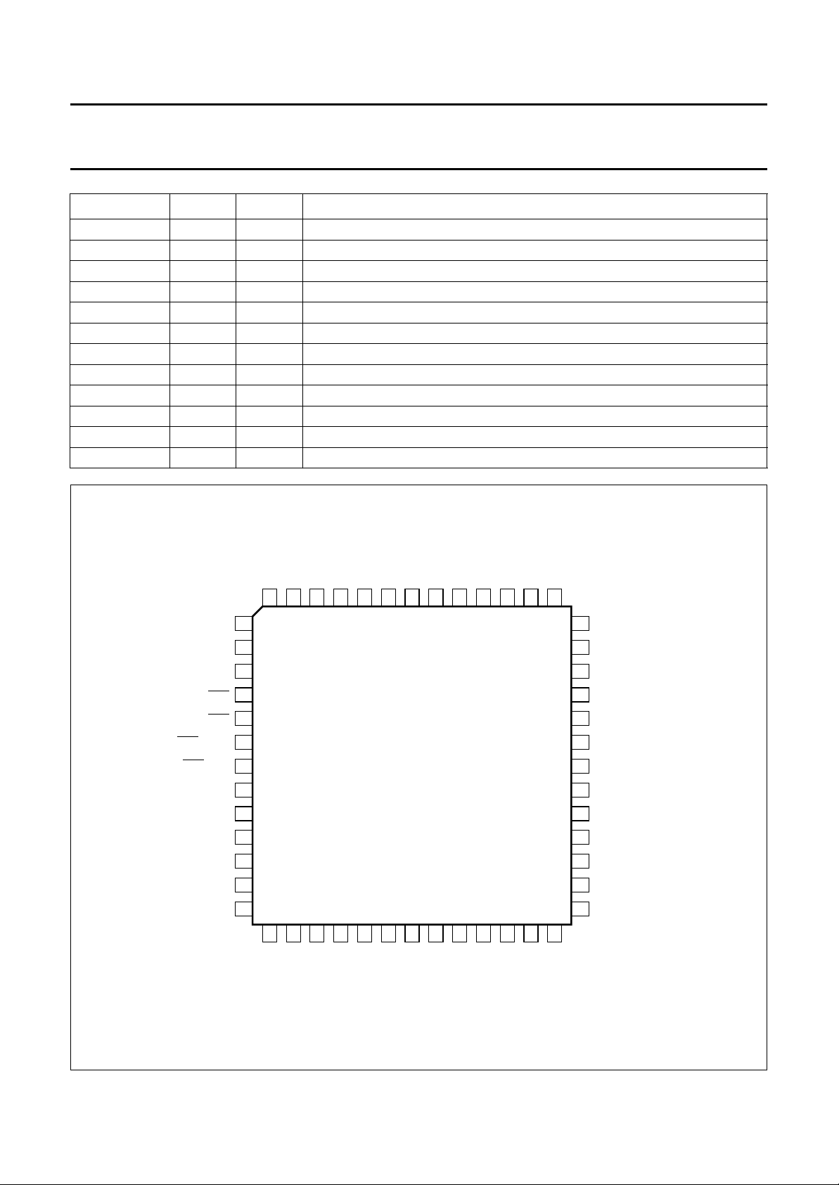
in a 52-pin PLCC package.
The TDA5147K (see Fig.1) is controlled by a custom
digital ASIC. The custom ASIC provides the necessary
commutation sequences for the spindle drivers via the
SCNTL1, SCNTL2 and SCNTL3 inputs. Spindle speed is
monitored by comparator outputs SENU, SENV and
SENWIS. Motor speed control is accomplished by a PWM
signal (input at the SIPWM pin).
Control of the VCM circuits is via the V
input signals. These two inputs provide control of the coil
current. The V
output signal can be used to monitor
ISENSE2
the voice coil current.
IPWMH
and V
IPWML
QUICK REFERENCE DATA
SYMBOL PARAMETER MIN. TYP. MAX. UNIT
Supply voltage
V
V
CCA1
CCA2
analog supply voltage 1 4.5 5.0 5.5 V
analog supply voltage 2 10.8 12.0 13.2 V
Drivers
I
spin(max)
I
VCM(max)
maximum spindle current − 1 − A
maximum voice coil motor current − 0.8 − A
ORDERING INFORMATION
TYPE
NUMBER
NAME DESCRIPTION VERSION
PACKAGE
TDA5147K PLCC52 plastic leaded chip carrier; 52 leads SOT238-2
1996 Jul 26 2
Page 3
Philips Semiconductors Product specification
12 V Voice Coil Motor (VCM) driver and
spindle motor drive combination chip
BLOCK DIAGRAMS
handbook, full pagewidth
POR
V
PCNTL
V
IPWMH
V
IPWML
V
DIGITAL
CIRCUIT
ISENS2
SCNTL1 to 3
SENU, SENV, SENWIS
SIPWM
TDA5147K
POWER-ON RESET
PARK
VOICE COIL
MOTOR DRIVE
SPINDLE
TDA5147K
ACTUATORS
MBH018
Overview
No external power drivers; dynamic braking for non-power down situations; 1 A spindle current; 0.8A VCM power driver; full-wave spindle mode,
POR monitors for both 5 and 12 V supplies; auto-park in the event of power-down.
Fig.1 System block diagram.
1996 Jul 26 3
Page 4
Philips Semiconductors Product specification
12 V Voice Coil Motor (VCM) driver and
spindle motor drive combination chip
handbook, full pagewidth
BSTFLT
SCNTL2
SCNTL3
20
10SCNTL1
11
14
3SMODE1
V
23SCOMP
DECODER
V
CCA1
25 21
UPPER
BOOSTER
LOGIC
CCA1
BSTCP2BSTCP1
U.H
U.H
V.H
V.L
W.H
W.L
brake
disable
M
COMP
PWM/LIN
V
CCS
to the VCM
output stages
l
comp
THERMAL
SWITCH
I
set
I
sense
control
amplifier
SPWMTC
15
PWM/LIN
PWM
U.H
U.L
V.H
V.L
W.H
W.L
DRIVER
DRIVER
DRIVER
DRIVER
DRIVER
DRIVER
disable
disable
brake
disable
disable
brake
disable
disable
brake
from POR block
V
CCS
TDA5147K
19
SHPWR3
51
SHPWR2
24
SDRVU
29
SHPWR1
C
clamp
12
SDRVV
2
SDRVW
I
13
V
I
sense
CCS
set
COMP
34
PGND150V
TDA5147K
I
COMP
CCA2
SISENL 32
SISENH 31
R
s
30SIPWM
26SPWMFLT
PWM
DECODER
FILTER
AMP
V
ref
Fig.2 Block diagram of spindle motor drivers.
1996 Jul 26 4
SISINK1, SISINK2
COMP
COMP
COMP
M
multiplexer
9
SISINK227SISINK145PGND2
SDRVU
SDRVV
SDRUW
16
18
17
MBH024
8
SDRVN
SENV
SENU
SENWIS
Page 5
Philips Semiconductors Product specification
12 V Voice Coil Motor (VCM) driver and
spindle motor drive combination chip
handbook, full pagewidth
V
CCS
V
POR12
ADJ
V
6
V
CCA2
CCAI
CCV
UNDER
VOLTAGE
GENERATOR
V
ref
C
1339
POR
4
PWM
DETECTOR
to spindle
section
POR
5
V
V
DD
DD
disable
V
PCNTL
35
park
autopark
V
ref(o)
SHPWR
PARK
CICUITRY
POWER
RET
22
ADJ
SDRU
TDA5147K
36
V
CMN
POR5
V
IPWML
V
IPWMH
V
V
ADJ
ref(o)
ref(i)
7
37
38
46
47
PWM
DECODER
AGND1
5228
AGND2
V
ref(o)
48
V
FLTINP
TDA5147K
V
ref(o)
V
CCA2
V
FLTOUT
3349
V
CMINP
POWER
POWER AMPLIFIERS
SENSE
V
ref(o)
41 44
V
ISEN2
SENSE
V
ref(o)
V
ISEN1
42VCMP
43
V
ISENL
40VISENH
M
R
s
MBH023
Fig.3 Block diagram of voice coil motor driver.
1996 Jul 26 5
Page 6

Philips Semiconductors Product specification
12 V Voice Coil Motor (VCM) driver and
spindle motor drive combination chip
PINNING
SYMBOL PIN I/O DESCRIPTION
V
CCA1
SDRVW 2 O phase 3 output for spindle motor
SMODE1 3 I 3-state level input for spindle mode
C
POR
POR 5 O power-on reset digital output (active LOW)
POR12
POR5
ADJ
ADJ
SENWIS 8 O digital output of back EMF sense 3/inductive sense
SISINK2 9 − connection 2 to the sense resistor
SCNTL1 10 I digital input 1 for spindle decoder
SCNTL2 11 I digital input 2 for spindle decoder
SDRVV 12 O phase 2 output for spindle motor
V
CCS
SCNTL3 14 I digital input 3 for spindle decoder
SPWMTC 15 O capacitor for spindle low side PWM time off
SDRVN 16 O centre TAP connection to spindle motor
SENU 17 O digital output of back EMF sense 1
SENV 18 O digital output of back EMF sense 2
SHPWR3 19 O capacitor 3 for PARK supply voltage
BSTFLT 20 O booster filter output
BSTCP2 21 O booster capacitor 2 output
RET
ADJ
SCOMP 23 O control amplifier pole adjustment
SDRVU 24 O phase 1 output for spindle motor
BSTCP1 25 O booster capacitor 1 output
SPWMFLT 26 O capacitor for spindle PWM filter
SISINK1 27 − connection 1 to the sense resistor
AGND1 28 − analog ground 1
SHPWR1 29 O capacitor 1 for PARK supply voltage
SIPWM 30 I digital PWM input for spindle current
SISENH 31 O sense resistor for spindle current
SISENL 32 O isolated ground connection for spindle sense amplifier
V
CMINP
PGND1 34 − power ground of VCM driver
V
PCNTL
V
CMN
V
ref(o)
V
ref(i)
V
CCV
V
ISENH
1 − analog supply voltage 1 (+5 V)
4 I/O power-on reset delay capacitor
6 O adjustment of POR threshold (for +12 V)
7 O adjustment of POR threshold (for +5 V)
13 − power supply of spindle motor drivers (+12 V)
22 I/O retract voltage adjustment pin
33 I closed loop voltage compensation of VCM
35 I PARK enable 3-state voltage level input
36 O negative output voltage of H-bridge
37 O reference voltage output for external ADC
38 I reference voltage input for the 2nd sense amplifier
39 − power supply of VCM driver (+12 V)
40 I positive input voltage of sense resistor amplifier
TDA5147K
1996 Jul 26 6
Page 7
Philips Semiconductors Product specification
12 V Voice Coil Motor (VCM) driver and
spindle motor drive combination chip
SYMBOL PIN I/O DESCRIPTION
V
ISENS2
V
CMP
V
ISENL
V
ISENS1
PGND2 45 − power ground 2 of voice coil motor driver
V
IPWML
V
IPWMH
V
FLTINP
V
FLTOUT
V
CCA2
SHPWR2 51 O capacitor for PARK supply voltage
AGND2 52 − analog ground 2
41 O voltage output 2 of sense resistor amplifier
42 O positive output voltage of H-bridge
43 I negative input voltage of sense resistor amplifier
44 O voltage output 1 of sense resistor amplifier
46 I PWM input voltage (LSB)
47 I PWM input voltage (MSB)
48 O voice coil motor PWM filter capacitor
49 O PWM filter output voltage
50 − analog supply voltage 2 (+12 V)
TDA5147K
handbook, full pagewidth
V
SDRVW
SMODE1
POR12
POR5
SENWIS
SISINK2
SCNTL1
SCNTL2
SDRVV
CCA1
C
POR
POR
ADJ
ADJ
V
CCS
CCA2VFLTOUTVFLTINPVIPWMHVIPWMLVISENS1
V
SHPWR2
AGND2
52
51
50
49
48
47
1
2
3
4
5
6
7
8
9
10
11
12
13
14
15
16
SCNTL3
SDRVN
SPWMTC
17
SENU
TDA5147K
18
19
SENV
SHPWR3
PGND2
46
45
20
21
BSTFLT
BSTCP2
44
22
ADJ
RET
ISENLVCMP
V
43
23
SCOMP
42
41
24
25
SDRVU
BSTCP1
ISENS2VISENH
V
40
39
38
37
36
35
34
33
32
31
30
29
28
27
26
MBH017
SPWMFLT
V
CCV
V
ref(i)
V
ref(o)
V
CMN
V
PCNTL
PGND1
V
CMINP
SISENL
SISENH
SIPWM
SHPWR1
AGND1
SISINK1
Fig.4 Pinning configuration.
1996 Jul 26 7
Page 8

Philips Semiconductors Product specification
12 V Voice Coil Motor (VCM) driver and
spindle motor drive combination chip
FUNCTIONAL DESCRIPTION
Spindle drivers
The spindle section contains both the low and high side
drivers (configured as H bridges) for a three-phase DC
brushless motor. Back EMF (BEMF) sensing of the
commutation rate needs to be output to an external digital
ASIC circuit. This digital circuit also provides the input
commutation control. Consequently, all speed control,
start-up routine and commutation control will be generated
by the digital circuit.
The SIPWM signal from the digital circuit is used to control
the spindle current. This PWM signal is internally filtered.
The output of this filter is duty factor dependent only. The
filter characteristics is that of a 1-pole low-pass filter, with
the pole location being controlled by the external capacitor
connected to pin SPWMFLT.
Dynamic braking is possible only during non power-down
situations and must be initiated by the digital circuit.
SMODE1
TDA5147K
to obtain high start-up torque. The purpose of the PWM
mode is to drive the low drivers into saturation (saturation
reduces the power dissipation in the TDA5147K during
start-up).
When the spindle current reaches the programmed set
current (SIPWM) value, a one-shot is fired. The output of
the one-shot remains high for the programmed off-time
) set by the capacitor/resistor network at the SPWMTC
(t
off
pin. The one-shot is not retriggerable for approximately
10% of the off-time, this gives a minimum of (10% t
time-on. During the off-time, the lower spindle output
drivers are switched off. The on-time of the drivers is not
fixed but is determined by the charging time of the coil
current to reach the program set current.
The turn-off time is calculated by the equation:
t
=R×C
off
Where R = 68 kΩ and C = 220 pF, t
ln(2)
= 10.4 µs.
off
The minimum on-time can be calculated by the equation:
CV
t
=
--------
on
I
)
off
A 3-state level mode line (SMODE1) has been included to
allow for;
1. An induction sensing algorithm in pre-start-up (V
2. PWM control during start-up (0.5V
CCA1
).
CCA1
3. Linear control (0 V).
S
ENSING MODE
The induction sensing mode is used for two purposes.
Firstly one of the BEMF sensor outputs (SENWIS) will be
shared with the voltage comparator that is used for the
induction sensing function. Prior to start-up each phase
can be excited for a short period of time. The current from
each coil can be monitored via the multiplexed output
(SENWIS). By comparing the rise times of each phase the
rotor position can be determined.
Secondly, in situations where the spindle motor requires
more current to spin-up, this mode is used with the
exception that the output SENWIS is ignored. Since, in the
induction sense mode, the output drivers are operated in
saturation mode, the motor current is limited only by the
power supply. This condition of induction sense mode can
be used to overcome the head friction and must be used
only when needed.
PWM M
ODE
INEAR MODE
L
The linear mode is used when the motor is near to its
).
intended speed. It can also be used at start-up, but higher
power dissipation will occur. In the linear mode the linear
drivers are controlled by a sensing amplifier. A Miller
network is used to obtain soft switching on the lower
drivers. This prevents large voltage spikes on the motor
coils when the lower drivers are switching. The high drivers
are switched into the linear (resistive) region.
The transconductance gain of the low driver current to filter
voltage can be calculated as follows:
G
m
I
coil
--------------------------- V
SPWMFLT
V
1
SISENH
------
--------------------------- -
R
V
s
SPWMFLT
==
1
-----R
s
For a 100% duty factor at SIPWM, the nominal voltage at
SPWMFLT = 1.74 V. The calculated coil current for a
100% duty factor (sense resistors R
1
1
I
coil
-----------
0.33
1.74 1.05 A=××=
-- 5
= 0.33 Ω) is:
s
Referencing to the duty factor, the coil current is:
I
coil
-----R
1.74
0% duty
××
--------------------100
1
1
-- 5
s
1
0.348()
-----R
s
1
A/V===
-- 5
0% duty
×== =
--------------------100
The PWM mode is normally used during the start-up
phase. Maximum drive voltage is applied to the low drivers
1996 Jul 26 8
Page 9
Philips Semiconductors Product specification
12 V Voice Coil Motor (VCM) driver and
TDA5147K
spindle motor drive combination chip
The duty factor is arranged so that at 100%, the voltage SPWMFLT = 1.74 V and at a 5% duty factor SPWMFLT = 0 V.
This is to ensure that at 0% duty factor the current will be zero (allowances for circuit tolerances).
The input decoder is driven by three lines which define the windings to be energized. The input decoder must then
translate these lines to six lines to drive the six output drivers. The truth table is given in Table 1.
Table 1 Input decoder truth table
(1)
CONDITION SCNTL1 SCNTL2 SCNTL3 SDRVU
SDRVV
Disable LOW LOW LOW X X X
Dynamic brake HIGH HIGH HIGH HIGH HIGH HIGH
State 1 HIGH HIGH LOW LOW X HIGH
State 2 HIGH LOW LOW X LOW HIGH
State 3 HIGH LOW HIGH HIGH LOW X
State 4 LOW LOW HIGH HIGH X LOW
State 5 LOW HIGH HIGH X HIGH LOW
State 6 LOW HIGH LOW LOW HIGH X
Under voltage −−−XXX
Note
1. X = 3-state.
(1)
SDRVW
(1)
VCM driver
The VCM driver is a linear, class AB, H-bridge type power
driver with all power devices internal to the chip. In addition
to the power stage a sense resistor enables VCM current
to be measured and brought out to a separate ADC via the
V
pin. The reference voltage for the V
ISENS2
ISENS2
output
is provided externally. The current level to the VCM is
controlled via two PWM signals that are generated by the
digital circuit. The input voltage at pin 47 (V
handbook, full pagewidth
PWM (MSD)
PWM (LSB)
LEVEL
CONVERTOR
LEVEL
CONVERTOR
V
IPWMH
ref
)
ATTENUATION
represents a weighting of 32 times more than the input
voltage at pin 46 (V
equal to 32 × duty factor (V
), thus the current command is
IPWML
IPWML+VIPWMH
). These PWM
signals are filtered by an internal 3rd-order low-pass filter
(Butterworth filter). The bandwidth of this low-pass filter is
nominally 40 kHz (less than 2 degrees lag at 500 Hz), but
the real pole may be adjustable by an external capacitor.
The analog output of the filter depends on the duty factor
of the PWM signal and not on the logic level.
32 : 1
SUM
UNITY
GAIN
LOW-PASS
MBH019
analog
output
Fig.5 Block diagram of the PWM filter.
1996 Jul 26 9
Page 10

Philips Semiconductors Product specification
12 V Voice Coil Motor (VCM) driver and
spindle motor drive combination chip
PARK ENABLE
A 3-state-level mode line (V
will:
1. Enable VCM drivers; V
2. Disable VCM drivers; 0.5V
3. PARK (soft retract the actuator); 0 V.
Enable VCM drivers
When the enable signal is HIGH, the VCM drivers are
controlled by the two PWM inputs. The two digital signals
convert the duty factor to a voltage level at V
100% duty factor the V
above V
. At a 0% duty factor the V
ref(o)
FLTINP
approximately −1 V below V
voltage level is equal to V
ref(o)
voltage is amplified, filtered and output at V
voltage at V
V
voltage, in conjunction with the sense resistor
FLTOUT
varies between ±2 V about V
FLTOUT
amplifier, drives the two VCM drivers as illustrated in Fig.8.
The transconductance equation that governs the voltage
to I
I
coil
R2
------- R1
is:
coil
–
1
Amps per Volt
×××=
-----R
s
==
from V
FLTINP
G
---------------------------------------------
m
V
1
2
-----------gain
FLTINPVref o()
In a typical application:
I
--------------------------------------------V
coil
–
FLTINPVref o()
2
-- 4
6.6 kΩ
×
-----------------10 kΩ
The transconductance is variable by selecting external
resistors R2/R1 and sense resistors R
Disable VCM drivers
With the PARK enable signal at 0.5V the VCM drivers are
disabled while the rest of the circuits remain enabled.
A sleep mode is initiated when the spindle and VCM are
disabled (this places the TDA5147K in its lowest power
setting).
) has been included that
PCNTL
(normal).
CCA1
.
CCA1
. At a
FLTOUT
voltage is approximately 1 V
voltage is
FLTINP
. At a 50% duty factor, the
ref(o)
(typical 4 V). The V
I
-----------------------------------------------------V
coil
FLTOUTVref o()
–()
1
× 1 Amp per Volt==
-----------
0.33
s
FLTOUT
FLTINP
. The
ref(o)
. The
TDA5147K
CTUATOR PARK
A
Retracting the actuator can be accomplished by driving
V
LOW in conjunction with either the spindle is
PCNTL
turning or a brake voltage has been applied. An adjustable
retract voltage of 1.2 V (max.) is applied between the V
and V
outputs. The retract circuit obtains its retract
CMP
current from the spindle SDRVU phase. If the SDRVU
phase is zero there will be no retract voltage.
The retract voltage is determined by two external resistors.
One end is tied to V
common point is tied to pin 22 (RET
and the other to ground. The
CMN
); see Fig.1 for
ADJ
additional information.
The calculation of V
V
RETRACT
Where 0.65 is V
0.65
BE
RETRACT
×=
at 25 °C ∆VBE/∆T=−2 mV/°C; 50 kΩ
is as follows:
1R2+
-----------------
R1
+
--------------- 50 kΩ
R2
can vary by ±30%
It should be noted that R2 has to be less than 10 kΩ.
Power-on reset
The power-on reset circuit monitors the voltage levels of
both the +5 V and the +12 V supply voltages as shown
in Fig.6. The
POR (active LOW) logic line is set HIGH
following a supply voltage rise above a specified voltage
threshold plus a hysteresis, and delayed by a time, tC that
is controlled by an external capacitor. This
POR signal
should remain HIGH until either the +5 or +12 V supplies
drop below the voltage threshold, at which point the
line should be asserted LOW.
The tC timing is set by the following equation:
CV
×
=
t
C
Where V
th
-----------------I
= 2.5 V and I is 12 µA (typ.).
th
A negative going pulse width of 5 µs on either the
+5 or +12 V rail will provide a full output pulse. If another
trigger pulse occurs before the output is completed a new
output pulse will be originated. This implies the power-on
reset circuit is a retriggerable one-shot with a maximum
trigger pulse of 5 µs (see Fig.7).
CMN
POR
1996 Jul 26 10
Page 11

Philips Semiconductors Product specification
12 V Voice Coil Motor (VCM) driver and
spindle motor drive combination chip
handbook, full pagewidth
V
CC
0.8 V
POR
V
hys
t
C
TDA5147K
MBH021
threshold
t
t
C
handbook, full pagewidth
V
CC
POR
Fig.6 Power-on reset timing.
threshold
1 V
5 µs
slopes 1 µs/V
t
C
t
hysteresis
MBH020
Fig.7 Trigger pulse requirement.
1996 Jul 26 11
Page 12

Philips Semiconductors Product specification
12 V Voice Coil Motor (VCM) driver and
TDA5147K
spindle motor drive combination chip
During a power-down situation the power-on reset circuit
must not only generate aPOR output signal, but must also
activate the VCM retract circuitry. In doing so, the VCM
driver draws power from the BEMF of the SDRVU output
during spin-down, and uses this power to bias the VCM
against one of the hard stops of the actuator. This prevents
the heads from landing on data zones. This BEMF supply
is isolated from the supply voltage for the drive, and is
half-wave rectified. An external retract capacitor is used to
provide the supply voltage for the retract circuit.
It should be noted that in both power-down retract and
command retract situations, the voltage across the VCM is
nominally limited to 1.2 V (to limit the velocity of the
actuator). Additional information is given in Fig.6.
LIMITING VALUES
In accordance with the Absolute Maximum Rating System (IEC 134).
SYMBOL PARAMETER CONDITIONS MIN. MAX. UNIT
V
V
V
V
T
T
T
CCA1
CCA2
o
n
stg
j
amb
analog supply voltage 1 indefinite time period −0.3 6.0 V
analog supply voltage 2 indefinite time period −0.3 13.5 V
output voltage (pins 2, 12 and 24) −0.3 20 V
output voltage on other pins −0.3 − V
IC storage temperature −55 +125 °C
maximum junction temperature − 150 °C
operating ambient temperature 0 70 °C
S
LEEP MODE
A sleep mode is used to save power when the spindle
drivers and the VCM drivers are in a disabled state. These
two conditions automatically turn off all drivers and
amplifiers that are not required. The total power dissipation
is approximately 100 mW. The sleep mode is activated
when both the spindle is disabled (SCNTL1, 2 and 3 = 0)
and the VCM is disabled (V
T
HERMAL SHUTDOWN
left open-circuit).
PCNTL
When the TDA5147K chip temperature is greater than
150 °C all power drivers will be automatically disabled.
This is to ensure that no fire hazard occurs due to chip
overheating.
note 1 −0.3 7.0 V
note 1 −0.3 15.0 V
Note
1. Stress beyond these levels may cause permanent damage to the device. This is a stress rating only and functional
operation of the device under this condition is not implied.
HANDLING
Inputs and outputs are protected against electrostatic discharge in normal handling. However, to be totally safe, it is
desirable to take normal precautions appropriate to handling MOS devices.
THERMAL CHARACTERISTICS
See report AA94052 (dated 94-02-03):
“PLCC52 - Thermal resistance evaluation”.
SYMBOL PARAMETER VALUE UNIT
T
th j-a
thermal resistance from junction to ambient in free air 30 K/W
1996 Jul 26 12
Page 13

Philips Semiconductors Product specification
12 V Voice Coil Motor (VCM) driver and
TDA5147K
spindle motor drive combination chip
OPERATING CHARACTERISTICS
V
=5V; V
CCA1
CCS=VCCA2=VCCV
SYMBOL PARAMETER CONDITIONS MIN. TYP. MAX. UNIT
Supplies
V
V
CCA1
CCS
analog supply voltage 1 4.5 5 5.5 V
supply voltage for spindle
motor drivers
V
V
CCV
CCA2
supply voltage for VCM driver 10.8 12 13.2 V
analog supply voltage 2 10.8 12 13.2 V
Reference voltage; pin 38 (V
V
ref(i)
reference voltage input 1.75 − 2.75 V
Upper booster
C
O
C
CP
external output capacitor connected between
charge pump capacitor connected between
ref(i)
= 12 V; T
)
= 0 to 70 °C; unless otherwise specified.
amb
10.8 12 13.2 V
− 10 − nF
BSTCP1 and BSTCP2
− 22 − nF
BSTFLT and ground
Spindle low side; pin 15 (SPWMTC)
C
sl
R
sl
capacitor for spindle low side − 220 − pF
resistor for spindle low side − 68 − kΩ
Capacitors for PARK voltage supply; pins 19 and 51 (SHPWR3 and SHPWR2)
C
clamp
clamp capacitor − 22 −µF
Digital PWM input; pin 30 (SIPWM)
V
IH
V
IL
HIGH level input voltage 3 5 5.5 V
LOW level input voltage −0.3 0 2 V
Digital inputs of spindle decoder; pins 10, 11 and 14 (SCNTL1, 2 and 3)
V
IH
HIGH level input voltage see Table 1; V
= 5 V 3.5 −−V
CCA1
3-state level input; pin 3 (SMODE1)
V
oh
V
iZ
3-state voltage level for current
sense in non PWM mode
3-state voltage level for BEMF
sense and PWM switch control
see Table 1; state also
achieved with floating
0.75V
CCA1
+ 150 mV
0.25V
CCA1
+ 150 mV
input
V
ol
3-state voltage level for BEMF
−−0.25V
sense and linear control
Control amplifier; pin 23 (SCOMP)
C
SCOMP
control loop capacitor − 47 − nF
−−V
0.50V
CCA1
0.75V
CCA1
V
− 150 mV
V
CCA1
− 150 mV
1996 Jul 26 13
Page 14

Philips Semiconductors Product specification
12 V Voice Coil Motor (VCM) driver and
TDA5147K
spindle motor drive combination chip
SYMBOL PARAMETER CONDITIONS MIN. TYP. MAX. UNIT
PARK enable; pin 35 (V
V
oh
V
iZ
V
ol
voltage level for enable 0.75
voltage level for disable see Table 1; state also
voltage level for retract −−0.25V
PWM decoder; pins 46 and 47 (V
V
IH
V
IL
f
PWM
HIGH level input voltage 3.0 −−V
LOW level input voltage −−2.0 V
frequency range at the inputs
of the PWM
T
PWM
PWM pulse width 25 −−ns
Sense resistor amplifier; pins 40 and 43 (V
V
iCM
common mode input sense
voltage
R
s(S)
spindle sense resistor − 0.33 −Ω
Power-on reset generator
C
POR
power-on reset capacitor see Fig.6 − 220 − nF
VCM PWM filter
C
FLTINP
filter capacitor − 1.8 − nF
VCM driver
R
s(VCM)
VCM sense resistor − 0.33 −Ω
PCNTL
)
VCCA1
−−V
+ 150 mV
achieved with floating
0.25V
+ 150 mV
CCA1
0.50V
CCA1
0.75V
CCA1
− 150 mV
V
input
V
CCA1
− 150 mV
IPWML
and V
C
ISENH
)
IPWMH
= 1.8 nF −−625 kHz
FLTINP
and V
ISENL
)
0 − 2V
ELECTRICAL CHARACTERISTICS
V
CCA1
=5V; V
CCS=VCCA2=VCCV
= 12 V; T
= 0 to 70 °C; note 1; unless otherwise specified.
amb
SYMBOL PARAMETER CONDITIONS MIN. TYP. MAX. UNIT
Analog supply current (nominal voltage)
I
CCA1
analog supply current 1 linear (no spindle or VCM load) − 5.0 8.0 mA
sleep mode (no spindle or VCM load) − 3.0 − mA
I
CCA2
analog supply current 2 linear (no spindle or VCM load) − 20 33 mA
sleep mode (no spindle or VCM load)
− 2.3 − mA
sense resistor output
sleep mode (no spindle or VCM load)
− 6.0 − mA
sense resistor input
P
tot
total power dissipation sleep mode −−150 mW
1996 Jul 26 14
Page 15

Philips Semiconductors Product specification
12 V Voice Coil Motor (VCM) driver and
TDA5147K
spindle motor drive combination chip
SYMBOL PARAMETER CONDITIONS MIN. TYP. MAX. UNIT
Voltage booster; pin 20 (BSTFLT)
V
oCP
charge pump output
voltage
I
oCP
charge pump output
current
Power monitor comparators; pins 6 and 7 (
V
th12
threshold voltage level
adjustment for +12 V
V
th5
threshold voltage level
adjustment for +5 V
V
hys1
hysteresis on V
CCA1
comparator
V
hys2
hysteresis on V
CCA2
comparator
V
12adj
power-on reset 12 V
adjustable voltage
V
5adj
power-on reset 5 V
adjustable voltage
nominal voltages 18.2 19.2 19.8 V
voltage drop of 100 mV across booster − 1.5 − mA
POR12
and POR5
ADJ
ADJ
)
8.7 9.0 9.3 V
4.4 4.5 4.6 V
hysteresis in positive direction. 40 60 80 mV
hysteresis in positive direction. 130 200 270 mV
normal power supply to resistor divider
3.25 3.32 3.39 V
25.4 and 9.7 kΩ
normal power supply to resistor divider
2.74 2.8 2.86 V
7.86 and 10 kΩ
Power-on reset generator; pins 4 and 5 (C
V
OL
LOW level input voltage IOL= 2 mA; VCC= 5 or 12 V
and POR); see Fig.6
POR
−−0.7 V
(below threshold voltage)
V
OH
HIGH level input voltage VCC=5or12V
4.85 −−V
(above hysteresis voltage)
I
source
source current for
8.2 12 15.3 µA
charging capacitor (pin 4)
V
th
t
dPOR
t
RPULSE
threshold voltage (pin 4) − 2.5 − V
power-on reset delay C = 220 nF − 45 − ms
power supply maximum
see Fig.7 − 2.5 5.0 µs
pulse duration
Thermal protection
T
Soff
switch-off temperature prevents fire hazard
150 − 164 °C
(junction temperature)
∆T thermal hysteresis − 30 −°C
Note
1. V
CCA2
, V
CCV
, V
CCS
and V
are connected together; the outputs SDRVU, SDRVV, SDRVW, VCMP and VCMN
CCA1
are not loaded. Sleep mode defined by 000 as spindle code and VCM disable.
1996 Jul 26 15
Page 16

Philips Semiconductors Product specification
12 V Voice Coil Motor (VCM) driver and
TDA5147K
spindle motor drive combination chip
SPINDLE MOTOR DRIVER CHARACTERISTICS
V
=5V; V
CCA1
CCS=VCCA2=VCCV
SYMBOL PARAMETER CONDITIONS MIN. TYP. MAX. UNIT
Overvoltage protection; pins 2, 12 and 24 (SDRVW, SDRVV and SDRVU)
V
CLP
overvoltage protection
clamping voltage
Spindle state control inputs; pins 10, 11 and 14 (SCNTL1, 2 and 3)
I
i
input current −10 − +10 µA
Back EMF comparators
V
CM
common mode input voltage
for centre TAP connection
(pin 16)
I
CLP
common mode clamping
current
V
Cos
comparator offset voltage
relative to pin 16
∆V
Cos
variation in comparator
voltages
V
sink
comparators output drive
sink voltage
V
source
comparators output drive
source voltage
= 12 V; T
= 0 to 70 °C; unless otherwise specified.
amb
power supply off; apply
− 19 − V
voltage to outputs; check
clamping voltage is at 100 mA
comparators will be
−0.5 − V
CCA2
+ 0.7 V
operational with other inputs
at V
CCA2
− 1V
V16=0V −1.6 −−0.2 mA
SDRVN voltage range from
−5 − +5 mV
3to10V
for the same IC −7 − +7 mV
I
=1mA −− 0.5 V
o(sink)
I
o(source)
=40µA 2.7 −− V
Spindle output drivers; pins 2, 12 and 24 (SDRVW, SDRVV and SDRVU)
R
I
LO
ds(on)
total resistance at output
(source + sink + isolation)
off-state output leakage
Io= 1 A at T
I
= 1 A at Tj= 125 °C − 1.3 1.7 Ω
o
=25°C − 0.8 1.0 Ω
amb
Tj= 125 °C − 0.3 1.0 mA
current
V
F
recirculating diode forward
IF=1A − 0.8 − V
voltage
SRT slew rate test test for Miller network 0.12 − 0.24 V/µs
Spindle current control PWM DAC and filter; pins 26 and 30 (SPWMFLT and SIPWM)
I
30
input current at pin 30 at HIGH-to-LOW voltage
−200 − +200 mA
transition
R
26
V
26
output resistance at pin 26 23 34 45 kΩ
output voltage 100% duty factor at pin 30 − 1.75 − V
50% duty factor at pin 30 − 0.85 − V
0% duty factor at pin 30 − 0 − V
1996 Jul 26 16
Page 17

Philips Semiconductors Product specification
12 V Voice Coil Motor (VCM) driver and
TDA5147K
spindle motor drive combination chip
SYMBOL PARAMETER CONDITIONS MIN. TYP. MAX. UNIT
PWM one-shot; pin 15 (SPWMTC)
I
sink
I
source
V
thST
V
thEND
t
off
t
on(min)
Current control loop and sense amplifier; pins 23 and 31 (SCOMP and SISENH)
V
i
I
SENSE
V
ratio
V
31
B
WD
Notes
1. Maximum current will be activated at 100% duty factor.
2. 5% duty factor guarantees current output.
3. Zero duty factor guarantees zero current output.
output sink current Vo= 3 V 600 850 1100 µA
output source current Vo=1V −−12 −µA
threshold voltage start level voltage for discharging 2.0 2.56 3.0 V
threshold voltage end level voltage for charging − 0.1 0.2 V
one-shot off time external network of R = 68 kΩ
− 10 −µs
and C = 220 pF
one-shot minimum on time external network of R = 68 kΩ
1 −− µs
and C = 220 pF
current sense amplifier
common mode input voltage
current sense amplifier input
current sense amplifier
operational over range
0 − 3.0 V
−10 −− µA
current
voltage ratio between
SPWMFLT and SISENH
output voltage at SENSH
(pin 31)
current loop bandwidth for
SPWMFLT to motor current
over sense resistance = 0.1
to 1 Ω
for 100% duty factor;
Rs= 0.33 Ω; note 1
for 50% duty factor;
= 0.33 Ω
R
s
for 5% duty factor;
= 0.33 Ω; note 2
R
s
for 0% duty factor;
= 0.33 Ω; note 3
R
s
Rs= 0.33 Ω, L
R
= 12.0 Ω
motor
motor
= 1 mH,
4.9 5.0 5.1 V/V
0.317 0.335 0.353 V
− 0.174 − V
0 0.018 0.026 V
0 0 1.0 mV
− 1 − kHz
1996 Jul 26 17
Page 18

Philips Semiconductors Product specification
12 V Voice Coil Motor (VCM) driver and
TDA5147K
spindle motor drive combination chip
VOICE COIL MOTOR DRIVER CHARACTERISTICS
V
=5V; V
CCA1
CCS=VCCA2=VCCV
SYMBOL PARAMETER CONDITIONS MIN. TYP. MAX. UNIT
Retract control voltage; pin 22 (RET
I
RET
t
h;RET
retract voltage load current V29= 9 V; power supplies
retract voltage hold time (power
down)
V
RET
retract voltage regulation nominal power supply at
VCM current control PWM DAC; pins 46 to 48 (V
I
47, 46
V
FL(p)
input current at pins 47 and 46 voltage range 0 to 5 V −200 − +200 µA
positive full scale DAC output
voltage at pin 48 relative to
pin 37
F
LI(n)
negative full scale DAC output
voltage at pin 48 relative to
pin 37
current ratio between MSB and
LSB
Z
o
output impedance from pin 48
to pin 37
= 12 V; T
ADJ
= 0 to 70 °C; unless otherwise specified.
amb
)
− 3.0 −µA
off
retract capacitor = 2.2 µF5 −−s
− 1.0 − V
T
=25°C
amb
power supply off;
= 9 to 2 V; V29= 7.5 V
V
24
, V
IPWML
IPWMH
and V
− 1.0 − V
)
FLTINP
100% duty factor − +1.0 − V
0% duty factor −−1.0 − V
31.5 32 32.5
1.40 2.0 2.6 kΩ
VCM PWM filter; pins 48 and 49 (V
I
o
output current on pin 49 V49= ∆Vo+ 10 mV 500 −−µA
∆Φ maximum phase shift from
pin 48 to pin 49
f
co
filter cut-off frequency from
pin 48 to pin 49
α
filter
filter attenuation at 1 MHz
measured from pin 48 to pin 49
V
49
output voltage range measured
at pin 49
Reference voltage; pin 37 (V
V
ref(o)
output reference voltage Io= 4 mA; CL= 10 nF 3.8 4.0 4.2 V
ref(o)
)
FLTINP
and V
FLTOUT
)
measured at 500 Hz;
= 1.8 nF
C
filter
pins 46 and 47 at 0% duty
factor
pins 46 and 47 at 50%
duty factor
pins 46 and 47 at 100%
duty factor
−−2 deg
− 40 − kHz
− 70 − dB
V37− 2.06 V37− 1.98 V37− 1.90 V
0.065 V
+ 1.90 V37+ 1.98 V37+ 2.06 V
V
37
37
0.065 V
1996 Jul 26 18
Page 19

Philips Semiconductors Product specification
12 V Voice Coil Motor (VCM) driver and
TDA5147K
spindle motor drive combination chip
SYMBOL PARAMETER CONDITIONS MIN. TYP. MAX. UNIT
Current sense amplifier; pins 38, 40, 41, 43 and 44 (V
I
40, 43
input current at pins 40 and 43 overvoltage range of
0to12V
I
sink1
output sink current 1 (pin 44) force V40− V43 to equal
−250 mV; allow output
drop of 100 mV between
no load and full load
I
source1
output source current 1 (pin 43) force V40− V43 to equal
−250 mV; allow output
drop of 100 mV between
no load and full load
V
40, 43
operating voltage range
gain and offset valid 0 − 12 V
(pins 40 and 43)
G1 amplifier gain for
− V37/V40− V
V
44
V
os1
B
G1
output offset voltage V40− V43= 0 V at 0.5V
unity gain bandwidth − 10 − MHz
43
PSRR power supply rejection ratio f
V
40, 43
operating voltage range
under all conditions 3.8 4.0 4.2 V/V
< 20 kHz − 60 − dB
i
gain and offset valid 0 − 12 V
(pins 40 and 43)
I
sink2
output sink current 2 (pin 41) force V40− V43 to equal
−250 mV; allow output
drop of 100 mV between
no load and full load
I
source2
output source current 2 (pin 43) force V40− V43 to equal
−250 mV; allow output
drop of 100 mV between
no load and full load
G2 amplifier gain for
V
− V38/V40− V
V
B
V
I
ref(i)
os2
G2
ref(i)
41
output offset voltage V40− V43= 0 V at 0.5V
unity gain bandwidth − 10 − MHz
input voltage level (pin 38) −−4.5 V
input current range (pin 38) Vi= 0 to 4.5 V − 0.06 1 µA
43
VCM output drivers; pins 33, 36 and 42 (V
R
tot
total output resistance
(source + sink + isolation)
I
LO
B
G
output leakage current Tj= 125 °C −−1mA
unity gain bandwidth from pin 33 to pins
under all conditions 3.8 4.0 4.2 V/V
, V
CMINP
T
T
CMN
=25°C − 1.0 1.25 Ω
amb
= 125 °C − 1.5 1.9 Ω
j
36 and 42
t
cro
crossover distortion time ramp input pin 33 = 20 µs − 25µs
, V
ref(i)
and V
ISENH
CMP
, V
ISENS2
, V
ISENL
and V
ISENS1
)
−200 415 540 µA
+400 −−µA
−−−400 µA
−15 − +15 mV
CC
+400 −−µA
−−−400 µA
−23 − +23 mV
CC
)
− 2 − MHz
1996 Jul 26 19
Page 20

Philips Semiconductors Product specification
12 V Voice Coil Motor (VCM) driver and
TDA5147K
spindle motor drive combination chip
SYMBOL PARAMETER CONDITIONS MIN. TYP. MAX. UNIT
RATIO =
/2
---- /1
L=
/2 /0–
--------------- /1 /0–
I
os
I
33
V
33
symmetry of VCM drivers
(pins 33 and 36)
linearity of VCM drivers
(pins 33 and 36)
VCM output offset current pins 47 and 46 at 50%
input current (pin 33) Vi= 0 to 10 V − 0.07 0.2 µA
input offset voltage (pin 33) from pin 33 to pin 37 −10 − +10 mV
I
2=IRVCM
at duty
factor = 10%;
I1=I
RCVM
at duty
factor = 90%;
I0=I
RCVM
at duty
factor = 50%; RS= 0.33 Ω;
R1=10kΩ, R2= 6.6 kΩ,
RL=15Ω
I
2=IRVCM
at duty
factor = 10%;
I1=I
RCVM
at duty
factor = 90%;
I0=I
RCVM
at duty
factor = 50%; RS= 0.33 Ω;
R1=10kΩ, R2= 6.6 kΩ,
RL=15Ω
duty factor; RS= 0.33 Ω;
R1=10kΩ, R2= 6.6 kΩ,
RL=15Ω
0.93 1 1.03
0.97 1 1.03
−28 0 +28 mA
1996 Jul 26 20
Page 21

Philips Semiconductors Product specification
12 V Voice Coil Motor (VCM) driver and
TDA5147K
spindle motor drive combination chip
MODE TABLES
Table 2 V
MODES OF OPERATION AT
POWER GOOD (
VCM enable HIGH X X X
VCM disable high impedance X X X
Park LOW X X X
Spindle enable X see Table 3 see Table 3 see Table 3
Spindle disable X LOW LOW LOW
Spindle brake X HIGH HIGH HIGH
Spindle mode high impedance LOW LOW LOW
Note
1. X = Don't care.
Table 3 Booster, driver, comparator, decoder, amplifier and filter modes
FUNCTION
Spindle enable ON ON ON ON ON
Spindle disable ON ON ON ON ON
POR LOW OFF OFF ON ON OFF
Sleep OFF OFF ON ON OFF
and SCNTL modes
PCNTL
POR = HIGH)
UPPER
BOOSTER
V
INPUT STATE
PCNTL
UPPER
DRIVERS
(1)
LOWER
DRIVERS
SCNTL INPUT STATES
SCNTL1 SCNTL2 SCNTL3
COMPARATOR
(1)
CONTROL
AMPLIFIER
Table 4
FUNCTION ONE-SHOT
Spindle enable ON ON ON ON ON ON
Spindle disable ON ON ON ON ON ON
POR LOW ON ON ON ON OFF ON
Sleep ON ON ON ON OFF ON
CURRENT
COMPARATOR
PWM
DECODER
FILTER
SMODE
COMPARATOR
CURRENT
SENSE
AMPLIFIER
LOGIC
DECODER
1996 Jul 26 21
Page 22

Philips Semiconductors Product specification
12 V Voice Coil Motor (VCM) driver and
spindle motor drive combination chip
(2)
(3)
SLEEP
FUNCTION
RETRACT CIRCUIT
THERMAL
SHUTDOWN
POR
DETECTOR
VOLTAGE
GENERATOR
TDA5147K
FILTER
AMPLIFIER
AMPLIFIER
VCM POWER
12 AND 5 V
COMPARATOR
SENSE2 SENSE1
Vref
OUTPUT
PWM DECODER
Vref
BUFFER
OUTPUT
ISREF
V
BUFFER
, PWM, power, POR, retract, reference, sense, thermal, voltage and sleep modes
3-STATE
VOLTAGE
LEVEL
ON ON ON ON ON OFF ON ON OFF
ISBUF
(1)
FUNCTION
VCM enable ON ON ON ON ON OFF
Table 5 V
1996 Jul 26 22
VCM Disable ON ON ON ON ON OFF
Park ON ON ON ON ON ON
Sleep OFF OFF ON OFF ON OFF
POR LOW OFF OFF ON OFF ON ON
Table 6
FUNCTION
VCM enable ON ON ON ON ON ON ON ON OFF
VCM disable ON ON ON ON ON OFF ON ON OFF
Park
Sleep ON OFF OFF OFF OFF OFF ON ON ON
POR LOW ON OFF OFF OFF OFF OFF ON ON ON
Notes
1. Park will provide adjustable retract if the spindle brake is on, or if the spindle brake is enabled.
2. If disable SP is OFF.
3. Requires disable SP and VCM disable to be ON.
Page 23

Philips Semiconductors Product specification
12 V Voice Coil Motor (VCM) driver and
spindle motor drive combination chip
book, full pagewidth
46
PWM
DEC
47
R2
48
33
V
ref(o)
R4
BUFFER
R1
0.5 V
R
CCV
TDA5147K
V
ref(o)
RR
R
49
36
R
I
COIL
42
R5
voice
M
coil
motor
V
ref(o)
R
R
43
40
MBH022
44
V1
V1
R4
Fig.8 Transconductance model.
1996 Jul 26 23
Page 24

Philips Semiconductors Product specification
12 V Voice Coil Motor (VCM) driver and
spindle motor drive combination chip
EQUATIONS
Gain from V
V
FLTOUTVref o()
----------------------------------------------V
FLTINPVref o()
–
–
Gain from V
V
FLTOUTVref o()
-----------------------------------------------
Gain of V
HAVE
SUB
–
R1
ISENS1
V1 V
–
-------------------------------
–
1V
--------------------------4R
Transconductance Equation
G
------------------------------------------
m
V
FLINPVref o()
to V
FLTINP
FLTOUT
2=
FLTOUT
to V
V
--------------------------------------------- -
(under closed loop V
ISENS1
ISENS1Vref o()
–
R2
relative to ∆Vs (voltage across Rs)
–
R
–
R
∆
V
--------- R
s
V1 V
SENS1
--------------------------------4R
∆
--------- -
s
×==
--------------------------------------------V
FLINTPVref o()
ref o()
4R
ref o()
I
COIL
–
V
ISENH
------------------ -
V
ISENLVISENH
------------------------------------------- -
CMINP=Vref(o)
V
FLTOUTVref o()
or
----------------------------------------------V
V
s
or
R
–
–
SENS1Vref o()
V
ISENL
==
-----------------R
V
SENS1Vref o()
--------------------------------------------
1
–
∆
–
V
s
TDA5147K
(1)
)
R1
==
------R2
4===
(2)
(3)
(4)
(5)
From equation (1)
From equation (2)
G
=
m
G
m
From equation (3) and (4)
Vs∆
--------- -
-------------------------------------------V
R
s
Vs∆
2
--------- R
s
G
m
2
–
FTOUTVref o()
R2
×× V
-------
SENS1Vref o()
R1
1
1
× 2
------
-- -
R
4
s
–()=
1
R2
××
------R1
1
R2
×==
×
-- 2
-----R
------- R1
s
1996 Jul 26 24
Page 25

Philips Semiconductors Product specification
12 V Voice Coil Motor (VCM) driver and
spindle motor drive combination chip
APPLICATION INFORMATION
ndbook, full pagewidth
V
CMN
digital
circuit
n.c.
12 V
0.47 µF
50 39 13
37
22
26
15
5
41
8
18
17
38
46
47
35
10
11
14
3
30
5 V
1202521
TDA5147K
C
APFLT
C
APCP
2319295152283445
TDA5147K
n.c.
7
n.c.
6
4
48
44
49
33
42
43
40
36
9
27
31
2
16
12
24
R
s
32
(1) (1)
C
POR
voice
coil
motor
(1)
spindle
motor
M
(1)
C
clamp
(1) Optional.
Fig.9 Application diagram.
1996 Jul 26 25
MBH025
Page 26

Philips Semiconductors Product specification
12 V Voice Coil Motor (VCM) driver and
spindle motor drive combination chip
PACKAGE OUTLINES
PLCC52: plastic leaded chip carrier; 52 leads
e
y
47
52
1
pin 1 index
D
X
3446
TDA5147K
SOT238-2
e
E
A
Z
E
33
b
p
b
1
w M
H
E
E
e
7
β
k
820
e
D
H
D
21
k
1
v M
Z
D
A
B
v M
B
0 5 10 mm
scale
DIMENSIONS (millimetre dimensions are derived from the original inch dimensions)
UNIT A
mm
inches
A
1
min. max. max. max. max.
4.57
0.51
4.19
0.180
0.020
0.165
A
0.25
0.01
A
4
3
3.05
0.12
b
0.53
0.33
0.021
0.013
b
p
1
0.81
0.66
0.032
0.026
(1)
D
19.15
19.05
0.754
0.750
(1)
E
eH
e
D
19.15
19.05
0.754
0.750
1.27
0.05
18.54
17.53
0.730
0.690
e
18.54
17.53
0.730
0.690
H
D
E
20.19
20.19
19.94
19.94
0.795
0.795
0.785
0.785
Note
1. Plastic or metal protrusions of 0.01 inches maximum per side are not included.
OUTLINE
VERSION
IEC JEDEC EIAJ
REFERENCES
SOT238-2
A
A
4
k
1
k
E
1.22
1.07
0.048
0.042
0.51
0.020
L
1.44
1.02
0.057
0.040
A
1
detail X
p
EUROPEAN
PROJECTION
(A )
3
L
p
(1) (1)
Z
Z
E
D
ywv β
0.18 0.100.18
0.007 0.0040.007
2.16
0.085
2.16
0.085
o
45
ISSUE DATE
92-10-08
95-02-25
1996 Jul 26 26
Page 27

Philips Semiconductors Product specification
12 V Voice Coil Motor (VCM) driver and
spindle motor drive combination chip
SOLDERING
Introduction
There is no soldering method that is ideal for all IC
packages. Wave soldering is often preferred when
through-hole and surface mounted components are mixed
on one printed-circuit board. However, wave soldering is
not always suitable for surface mounted ICs, or for
printed-circuits with high population densities. In these
situations reflow soldering is often used.
This text gives a very brief insight to a complex technology.
A more in-depth account of soldering ICs can be found in
our
“IC Package Databook”
Reflow soldering
Reflow soldering techniques are suitable for all PLCC
packages.
The choice of heating method may be influenced by larger
PLCC packages (44 leads, or more). If infrared or vapour
phase heating is used and the large packages are not
absolutely dry (less than 0.1% moisture content by
weight), vaporization of the small amount of moisture in
them can cause cracking of the plastic body. For more
information, refer to the Drypack chapter in our
Reference Handbook”
Reflow soldering requires solder paste (a suspension of
fine solder particles, flux and binding agent) to be applied
to the printed-circuit board by screen printing, stencilling or
pressure-syringe dispensing before package placement.
Several techniques exist for reflowing; for example,
thermal conduction by heated belt. Dwell times vary
between 50 and 300 seconds depending on heating
method. Typical reflow temperatures range from
215 to 250 °C.
(order code 9398 652 90011).
“Quality
(order code 9397 750 00192).
TDA5147K
Wave soldering
Wave soldering techniques can be used for all PLCC
packages if the following conditions are observed:
• A double-wave (a turbulent wave with high upward
pressure followed by a smooth laminar wave) soldering
technique should be used.
• The longitudinal axis of the package footprint must be
parallel to the solder flow.
• The package footprint must incorporate solder thieves at
the downstream corners.
During placement and before soldering, the package must
be fixed with a droplet of adhesive. The adhesive can be
applied by screen printing, pin transfer or syringe
dispensing. The package can be soldered after the
adhesive is cured.
Maximum permissible solder temperature is 260 °C, and
maximum duration of package immersion in solder is
10 seconds, if cooled to less than 150 °C within
6 seconds. Typical dwell time is 4 seconds at 250 °C.
A mildly-activated flux will eliminate the need for removal
of corrosive residues in most applications.
Repairing soldered joints
Fix the component by first soldering two diagonallyopposite end leads. Use only a low voltage soldering iron
(less than 24 V) applied to the flat part of the lead. Contact
time must be limited to 10 seconds at up to 300 °C. When
using a dedicated tool, all other leads can be soldered in
one operation within 2 to 5 seconds between
270 and 320 °C.
Preheating is necessary to dry the paste and evaporate
the binding agent. Preheating duration: 45 minutes at
45 °C.
1996 Jul 26 27
Page 28

Philips Semiconductors Product specification
12 V Voice Coil Motor (VCM) driver and
TDA5147K
spindle motor drive combination chip
DEFINITIONS
Data sheet status
Objective specification This data sheet contains target or goal specifications for product development.
Preliminary specification This data sheet contains preliminary data; supplementary data may be published later.
Product specification This data sheet contains final product specifications.
Limiting values
Limiting values given are in accordance with the Absolute Maximum Rating System (IEC 134). Stress above one or
more of the limiting values may cause permanent damage to the device. These are stress ratings only and operation
of the device at these or at any other conditions above those given in the Characteristics sections of the specification
is not implied. Exposure to limiting values for extended periods may affect device reliability.
Application information
Where application information is given, it is advisory and does not form part of the specification.
LIFE SUPPORT APPLICATIONS
These products are not designed for use in life support appliances, devices, or systems where malfunction of these
products can reasonably be expected to result in personal injury. Philips customers using or selling these products for
use in such applications do so at their own risk and agree to fully indemnify Philips for any damages resulting from such
improper use or sale.
1996 Jul 26 28
Page 29

Philips Semiconductors Product specification
12 V Voice Coil Motor (VCM) driver and
spindle motor drive combination chip
NOTES
TDA5147K
1996 Jul 26 29
Page 30

Philips Semiconductors Product specification
12 V Voice Coil Motor (VCM) driver and
spindle motor drive combination chip
NOTES
TDA5147K
1996 Jul 26 30
Page 31

Philips Semiconductors Product specification
12 V Voice Coil Motor (VCM) driver and
spindle motor drive combination chip
NOTES
TDA5147K
1996 Jul 26 31
Page 32

Philips Semiconductors – a worldwide company
Argentina: see South America
Australia: 34 Waterloo Road, NORTH RYDE, NSW 2113,
Tel. +61 2 9805 4455, Fax. +61 29805 4466
Austria: Computerstr. 6, A-1101 WIEN, P.O. Box 213,
Tel. +43 1 60 101, Fax. +43 1 60 101 1210
Belarus: Hotel Minsk Business Center, Bld. 3, r. 1211, Volodarski Str.6,
220050 MINSK, Tel. +375 172 200 733, Fax. +375 172 200773
Belgium: see The Netherlands
Brazil: see South America
Bulgaria: Philips Bulgaria Ltd., Energoproject, 15th floor,
51 James Bourchier Blvd., 1407 SOFIA,
Tel. +359 2 689 211, Fax. +359 2689 102
Canada: PHILIPS SEMICONDUCTORS/COMPONENTS,
Tel. +1 800 234 7381
China/Hong Kong: 501 Hong Kong Industrial Technology Centre,
72 Tat Chee Avenue, Kowloon Tong, HONG KONG,
Tel. +852 2319 7888, Fax. +8522319 7700
Colombia: see South America
Czech Republic: see Austria
Denmark: Prags Boulevard 80, PB 1919, DK-2300 COPENHAGEN S,
Tel. +45 32 88 2636, Fax. +45 31 57 1949
Finland: Sinikalliontie 3, FIN-02630 ESPOO,
Tel. +358 615 800, Fax. +358 615 80920
France: 4 Rue du Port-aux-Vins, BP317, 92156 SURESNES Cedex,
Tel. +33 1 40 99 6161, Fax. +33 1 4099 6427
Germany: Hammerbrookstraße 69, D-20097 HAMBURG,
Tel. +49 40 23 53 60, Fax. +4940 23536 300
Greece: No. 15, 25th March Street, GR 17778 TAVROS,
Tel. +30 1 4894 339/911, Fax. +30 14814 240
Hungary: see Austria
India: Philips INDIA Ltd, Shivsagar Estate, A Block, Dr. Annie Besant Rd.
Worli, MUMBAI 400 018, Tel. +91 22 4938541, Fax.+91 224938 722
Indonesia: see Singapore
Ireland: Newstead, Clonskeagh, DUBLIN 14,
Tel. +353 1 7640 000, Fax.+353 17640 200
Israel: RAPAC Electronics, 7 Kehilat Saloniki St, TEL AVIV 61180,
Tel. +972 3 645 0444, Fax.+972 3649 1007
Italy: PHILIPS SEMICONDUCTORS, Piazza IV Novembre 3,
20124 MILANO, Tel. +39 2 6752 2531, Fax. +392 67522557
Japan: Philips Bldg 13-37, Kohnan 2-chome, Minato-ku, TOKYO 108,
Tel. +81 3 3740 5130, Fax. +81 33740 5077
Korea: Philips House, 260-199 Itaewon-dong, Yongsan-ku, SEOUL,
Tel. +82 2 709 1412, Fax. +82 2 709 1415
Malaysia: No. 76 Jalan Universiti, 46200 PETALING JAYA, SELANGOR,
Tel. +60 3 750 5214, Fax. +603 7574880
Mexico: 5900 Gateway East, Suite 200, EL PASO, TEXAS 79905,
Tel. +9-5 800 234 7381
Middle East: see Italy
Netherlands: Postbus 90050, 5600 PB EINDHOVEN, Bldg. VB,
Tel. +31 40 27 82785, Fax.+31 4027 88399
New Zealand: 2 Wagener Place, C.P.O. Box 1041, AUCKLAND,
Tel. +64 9 849 4160, Fax. +64 9 849 7811
Norway: Box 1, Manglerud 0612, OSLO,
Tel. +47 22 74 8000, Fax. +47 22 74 8341
Philippines: Philips Semiconductors Philippines Inc.,
106 Valero St. Salcedo Village, P.O. Box2108 MCC,MAKATI,
Metro MANILA, Tel. +63 2 816 6380, Fax. +632 817 3474
Poland: Ul. Lukiska 10, PL 04-123 WARSZAWA,
Tel. +48 22 612 2831, Fax.+48 22612 2327
Portugal: see Spain
Romania: see Italy
Russia: Philips Russia, Ul. Usatcheva 35A, 119048 MOSCOW,
Tel. +7 095 926 5361, Fax.+7 095564 8323
Singapore: Lorong 1, Toa Payoh, SINGAPORE 1231,
Tel. +65 350 2538, Fax. +65 251 6500
Slovakia: see Austria
Slovenia: see Italy
South Africa: S.A. PHILIPS Pty Ltd., 195-215 Main Road Martindale,
2092 JOHANNESBURG, P.O. Box 7430 Johannesburg 2000,
Tel. +27 11 470 5911, Fax.+27 11470 5494
South America: Rua do Rocio 220, 5th floor, Suite 51,
04552-903 São Paulo, SÃO PAULO - SP, Brazil,
Tel. +55 11 821 2333, Fax.+55 11829 1849
Spain: Balmes 22, 08007 BARCELONA,
Tel. +34 3 301 6312, Fax. +34 3 301 4107
Sweden: Kottbygatan 7, Akalla, S-16485 STOCKHOLM,
Tel. +46 8 632 2000, Fax. +46 8 632 2745
Switzerland: Allmendstrasse 140, CH-8027 ZÜRICH,
Tel. +41 1 488 2686, Fax. +41 1 481 7730
Taiwan: PHILIPS TAIWAN Ltd., 23-30F, 66,
Chung Hsiao West Road, Sec. 1, P.O. Box 22978,
TAIPEI 100, Tel. +886 2 382 4443, Fax.+886 2382 4444
Thailand: PHILIPS ELECTRONICS (THAILAND) Ltd.,
209/2 Sanpavuth-Bangna Road Prakanong, BANGKOK 10260,
Tel. +66 2 745 4090, Fax. +66 2 398 0793
Turkey: Talatpasa Cad. No. 5, 80640 GÜLTEPE/ISTANBUL,
Tel. +90 212 279 2770, Fax. +90 212 282 6707
Ukraine: PHILIPS UKRAINE, 4 Patrice Lumumba str., Building B, Floor 7,
252042 KIEV, Tel. +380 44 264 2776, Fax. +38044 2680461
United Kingdom: Philips Semiconductors Ltd., 276 Bath Road, Hayes,
MIDDLESEX UB3 5BX, Tel. +44 181 730 5000, Fax.+44 181754 8421
United States: 811 East Arques Avenue, SUNNYVALE, CA 94088-3409,
Tel. +1 800 234 7381
Uruguay: see South America
Vietnam: see Singapore
Yugoslavia: PHILIPS, Trg N. Pasica 5/v, 11000 BEOGRAD,
Tel. +381 11 825 344, Fax.+38111 635777
For all other countries apply to: Philips Semiconductors, Marketing & Sales Communications,
Building BE-p, P.O. Box 218, 5600 MD EINDHOVEN, TheNetherlands, Fax.+31 4027 24825
© Philips Electronics N.V. 1996 SCA51
All rights are reserved. Reproduction in whole or in part is prohibited without the prior written consent of the copyright owner.
The information presented in this document does not form part of any quotation or contract, is believed to be accurate and reliable and may be changed
without notice. No liability will be accepted by the publisher for any consequence of its use. Publication thereof does not convey nor imply any license
under patent- or other industrial or intellectual property rights.
Printed in The Netherlands 397021/1200/01/pp32 Date of release: 1996 Jul26 Document order number: 9397 750 00988
Internet: http://www.semiconductors.philips.com
(1) TDA5147K_1 July 18, 1996 12:44 pm
 Loading...