

Page 1

INTEGRATED CIRCUITS
TDA5146T
Brushless DC motor drive circuit
Product specification 1994 May 18
Page 2

Philips Semiconductors Product specification
Type number
TDA5146TBrushless DC motor drive circuit
FEATURES
•Full–wave commutation (using push/pull drivers at the output stages) without position sensors
•Built–in start–up circuit
•Three push–pull outputs:
– 2 A output current (Typical)
– Built–in current limiter
•Thermal protection
•Soft switching outputs
•Flyback diodes
•Tacho output sensor
•Brake function
•Direction control input
•Reset function
•FET driver stage to be used in a buck converter
APPLICATIONS
General purpose spindle driver (e.g., HDD, tape driver)
GENERAL DESCRIPTION
The TDA5146T is a bipolar integrated circuit used to drive brushless DC motors in full–wave mode. The device senses the rotor position using
an EMF –sensing technique and is ideally suited as a drive circuit for a hard disk drive motor or tape drive.
QUICK REFERENCE DATA
Measured over full voltage and temperature ranges
Symbol
V
P
Vsup Supply for the FET driver voltage range 4 – 18 V
V
VMOT
VDo Driver output voltage drop IO= 100 mA – 0.9 1.05 V
I
LIM
NOTES:
1. An unstabilized supply can be used
2. V
VMOT=VP
; all outputs IO = 0 mA
Parameter Min. Typ. Max. Unit
Supply voltage range (Note 1) 4 – 18 V
Input voltage to the output driver stages (see Fig. 1) 1.7 – 16 V
Current limiting 1.80 2.0 2.5 A
ORDERING AND PACKAGE INFORMA TION
Package
Name Description Version
TDA5146T SO28 plastic small outline package; 28 leads; body width 7.5 mm SOT136-1
1994 May 18
2
Page 3
Philips Semiconductors Product specification
TDA5146TBrushless DC motor drive circuit
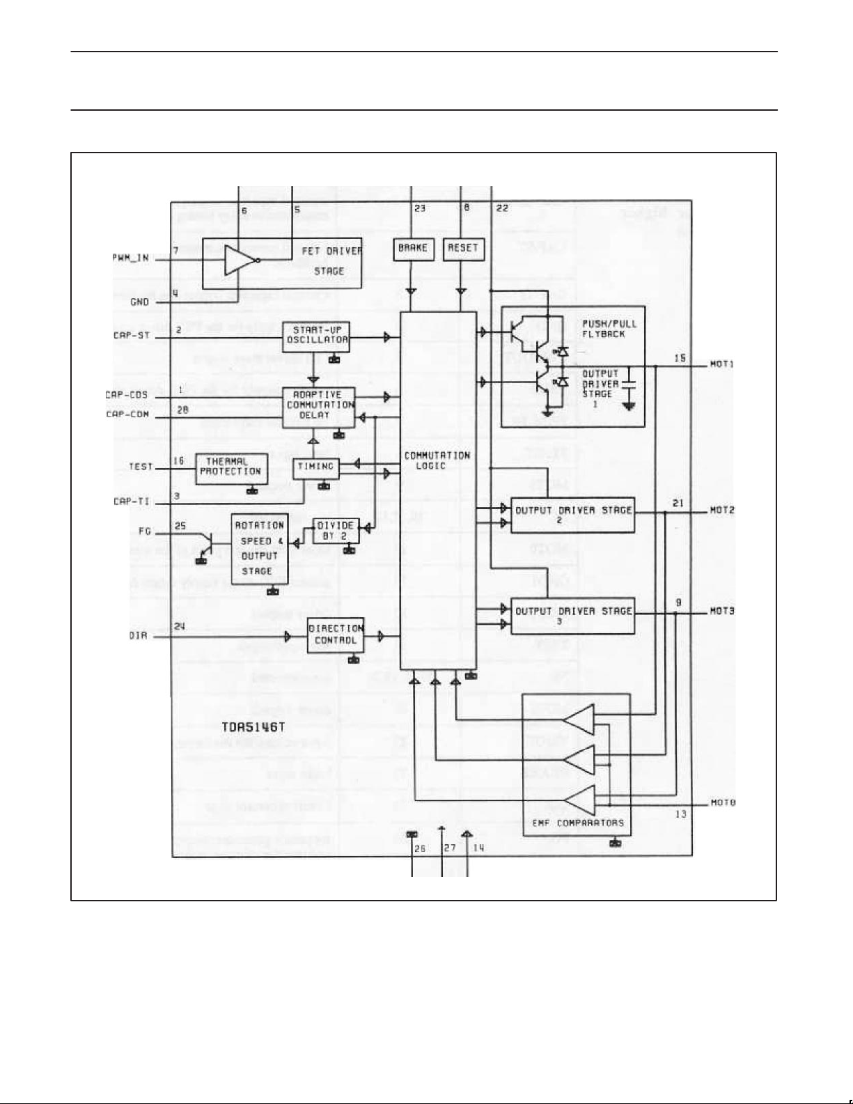
VSUP PWMOUT BRAKE RESET VMOT
1994 May 18
GND2 VP GND1
Figure 1. Block diagram
3
Page 4

Philips Semiconductors Product specification
TDA5146TBrushless DC motor drive circuit
PINNING
Symbol Pin Description
CAP–CDS 1 external capacitor connection for adaptive commutation delay timing copy
CAP–ST 2 external capacitor connection for start–up oscillator
CAP–TI 3 external capacitor connection for timing
GND 4 ground supply for the FET driver stage
PWMOUT 5 FET driver stage output
V
SUP
PWM_IN 7 FET driver stage input
RESET 8 reset input
MOT3 9 driver output 3
NC 10,1 1,12 not connected
MOT0 13 input from the star point of the motor coils
GND1 14 ground (0 V) motor supply return for output stages
MOT1 15 driver output 1
TEST 16 test input/output
NC 17,18,19,20 not connected
MOT2 21 driver output 2
VMOT 22 input voltage for the output driver stages
BRAKE 23 brake input
DIR 24 direction control input
FG 25 frequency generator: output of the rotation speed and position detector stages (open collector digi-
GND2 26 ground supply return for control circuits
V
P
CAP–CDM 28 external capacitor connection for adaptive commutation delay timing
NOTE:
1. Pins 10,11,12,17,18,19 have to be connected to the ground for higher dissipation
6 positive supply for the FET driver stage
tal output, negative – going edge is valid)
27 positive supply voltage
1994 May 18
CAP–CDS
CAP–ST
PWMOUT
PWM_IN
1
2
3
CAP–TI
4
GND
5
6
V
SUP
7
8
RESET
9
MOT3
10
NC
11
NC
12 17
NC
13 16
MOT0
14 15
GND1
Figure 2. Pin configuration
4
28
27
26
25
24
23
22
21
20
19
18
CAP–CDM
V
P
GND2
FG
DIR
BRAKE
V
MOT
MOT2
NC
NC
NC
NC
TEST
MOT1
SL01520
Page 5

Philips Semiconductors Product specification
TDA5146TBrushless DC motor drive circuit
FUNCTIONAL DESCRIPTION
The TDA5146T offers a sensorless three phase motor drive function. It is unique in its combination of sensorless motor drive and full–wave
drive.
The TDA5146T offers protected outputs capable of handling high currents and can be used with star or delta connected motors. It can easily be
adapted for different motors and applications. The TDA5146T offers the following features:
•Sensorless commutation by using the motor EMF
•Built–in start–up circuit
•Optimum commutation, independent of motor type or motor loading
•Built–in flyback diodes
•Three phase full–wave drive
•High output current (1.8 A)
•Outputs protected by current limiting and thermal protection of each output transistor
•Low current consumption by adaptive base–drive
•Soft switching pulse output for low radiation.
•Accurate frequency generator (FG) by using the motor BMF
•Direction of rotation controlled by one pin.
•FET driver stage to be used in a buck converter
LIMITING VALUES
In accordance with the Absolute Maximum System (IEC 134).
VP, V
V
I
V
VMOT
V
O
V
O
V
I
T
stg
T
amb
P
tot
Symbol
sup
Supply voltage – 18 V
Input voltage; all pins except VMOT (VI <18 V) –0.3 VP+0.5 V
V
input voltage –0.5 17 V
VMOT
Output voltage; PWM_OUT and PG/FG GND V
Output voltage MOT0, MOT1, MOT2 and MOT3 –1 V
Input voltage CAP–ST, CAP–TI, CAP–CD and CAP–DC – 2.5 V
Storage temperature range –55 +150 °C
Operating ambient temperature range 0 70 °C
Total power dissipation – – –
Parameter Min Max Unit
P
VMOT
+ V
V
V
D
HANDLING
Every pin withstands the ESD test according to MIL–STD–883C cross 1. Method 3015 (HBM 1500W, 100 pF 3 pulses + and 3 pulses – on each
pin referenced to ground.
1994 May 18
5
Page 6

Philips Semiconductors Product specification
TDA5146TBrushless DC motor drive circuit
3.5
3.0
2.5
P
tot
2.0
(H)
1.5
1.0
0.5
0
0 10203040506070
(o)
T
amb
Figure 3. Power derating curve (SOT136-1)
SL01519
1994 May 18
6
Page 7

Philips Semiconductors Product specification
TDA5146TBrushless DC motor drive circuit
CHARACTERISTICS
VP = 14.5 V; T
Symbol
Supply
V
P
I
P
V
VMOT
IVsup Vsup current range Vsup = 12 V – 1.2 2.0 mA
Thermal protection
T
SD
DT
MOT0 – CENTER TAPE
V
I
I
I
±V
CSW
DV
CS
V
H
MOT1, MOT2 AND MOT3
V
DO
DV
OL
DV
OH
I
LIM
Tr Rise time switching output VMOT=15V note 6 5 10 15
TF Fall time switching output VMOT=15V note 6 10 15 20
V
DHF
V
DLF
I
DM
DIR
V
IH
V
IL
I
IL
I
IH
RESET
V
IH
V
IL
I
IH
I
IL
= 25 °C; unless otherwise specified
amb
Parameter Conditions Min Typ Max Unit
Supply voltage range note 1 4 – 18 V
Input current range note 2 – 5.9 7.5 mA
Input voltage to the driver output
see Figure 1 1.7 – 16 V
stages range
Local temperature at temperature
130 140 150 °C
sensor causing shut–down
Reduction in temperature
after shut–down – TSD–30 – °C
before switch–on
Input voltage range –0.5 – V
VMOT
Input bias current 0.5 V<VI <VMOT–1.5 V –10 – –
Comparator Switching Level note 3 20 25 30 mV
Variation in threshold voltage be-
note 3 – – 3 mV
tween comparators
Comparator input hysteresis – 75 –
Dropout Voltage IO = 100 mA
IO =1000 mA
Variation in saturation voltage be-
IO = 100 mA – – 180 mV
– 0.9
1.6
1.05
1.85
tween lower transistors
Variation in saturation voltage be-
IO = –100 mA – – 180 mV
tween upper transistors
Current limiting V
Diode forward voltage (DH) notes 4 and 5;
=10V
VMOT
Rout=1.2W
1.8 2.0 2.5 A
– – 1.5 V
see Fig. 1;
I
= –500 mA
0
Diode forward voltage (DL) notes 4 and 5;
–1.5 – – V
see Fig. 1;
I
= 500 mA
0
Peak diode current note 5 – – 2.5 A
Normal rotation voltage on pin 5 4V< VP <18V 2.0 – – V
Reverse rotation voltage on pin 5 4V<VP <18V – – 0.8 V
Reverse rotation current – –20 –
Normal rotation current – –20 –
Input voltage HIGH in reset mode 4V< VP <18V 2.0 – – V
Input voltage LOW in normal mode 4V<VP <18V – – 0.8 V
Input current HIGH VI = 2.0 V – –20 –
Input current LOW VI = 0.8V – –20 –
V
mA
mV
V
ms
ms
mA
mA
mA
mA
1994 May 18
7
Page 8

Philips Semiconductors Product specification
TDA5146TBrushless DC motor drive circuit
Symbol UnitMaxTypMinConditionsParameter
BRAKE
V
IH
V
IL
I
IH
I
IL
FG
V
OL
V
OHmax
t
THL
d
PWM_IN
V
IH
V
IL
I
IH
I
IL
PWMOUT
V
0H
V
OL
I
pwmoutsource
I
pwmoutsink
SR PWM Output Slew Rate
CAP–ST
I
I
I
O
V
SWL
V
SWM
V
SWH
CAP–TI
I
I
I
OH
I
OL
V
SWL
V
SWM
V
SWH
Input voltage HIGH in brake mode 4V< VP <18V 2.0 – – V
Input voltage LOW in normal mode 4V<VP<18V – – 0.8 V
Input current HIGH VI = 2.0 V – –20 –
Input current LOW VI = 0.8 V – –20 –
mA
mA
Output voltage LOW IO =1.6 mA – – 0.4 V
Maximum output voltage HIGH V
Transition time HIGH–to–LOW
C
= 50 pF
L
R
= 10 kW
L
Ratio of FG frequency and
P
– 0.5 –
– 1:2 –
– – V
mS
commutation frequency
Duty factor – 50 – %
High Level Input 4V <VP < 18V 2.0 – – V
Low Level Input 4V <VP<18V – – 0.8 V
High Level Input Current VI =2.0V –3 0 3
Low Level Input Current VI =0.8V –20 –3 –
PWM Output HIGH PWM IN
<=2.0V
PWM Output LOW PWM IN
Vsup–
– – V
0.7
– – 0.7 V
mA
mA
>–0.8V
Sourcing capability PWMOUT=
10
9.5V
9V
5
15
30
mA
mA
mA
sinking capability PWMOUT=1V 25 – – mA
Rs=51 W
– 100 –
V/ mS
C1=2nF
Output sink current 1.6 2.1 2.6
Output source current –2.6 –2.1 –1.6
mA
mA
Lower switching level – 0.20 – V
Middle switching level – 0.30 – V
Upper switching level – 2.20 – V
Output sink current – 28 –
Output source current HIGH – –57 –
Lower source current LOW – –5 –
mA
mA
mA
Lower switching level – 50 – mV
Middle switching level – 0.30 – V
Upper switching level – 2.20 – V
1994 May 18
8
Page 9

Philips Semiconductors Product specification
TDA5146TBrushless DC motor drive circuit
Symbol UnitMaxTypMinConditionsParameter
CAP–CDM
l
I
I
O
II/I
O
V
IL
V
IH
CAP–CDS
I
I
I
O
II/I
O
V
IL
V
IH
NOTES:
1. An unstabilized supply can be used.
2. V
3. Switching levels with respect to MOT1, MOT2 and MOT3. See Figure 4.
4. Drivers are in high impedance OFF–state.
5. The outputs are short–circuit protected by limiting the current and the IC temperature.
6. Output transition time measurement. See Figure 5.
= VP, all other inputs at 0V; all outputs at VP and IO = 0mA.
MOT
Output sink current 10.6 16.2 22
Output source current –5.3 –8.1 –11
Ratio of sink to source current 1.85 2.05 2.25
Input voltage level LOW 0.85 – 0.9 V
Input voltage level HIGH 2.3 2.4 2.55 V
Output sink current 10.1 15.5 20.9
Output source current –20.9 –15.5 –10.1
Ratio of sink to source current 0.9 1.025 1.15
Input voltage level LOW 0.85 – 0.9 V
Input voltage level HIGH 2.3 2.4 2.55 V
mA
mA
mA
mA
mA
m
MOT 1 MOT 2 and MOT 3
Comparators threshold voltage
Figure 4.
Figure 5.
1994 May 18
9
Page 10

Philips Semiconductors Product specification
TDA5146TBrushless DC motor drive circuit
1. Value selected for 3 HZ start–up oscillator frequency
Figure 6. Application diagram without use of the FET driver stage
APPLICATION INFORMATION
Introduction
Full–wave driving of a three phase motor requires three push–pull output stages. In each of the six possible states two outputs are active, one
sourcing and one sinking current. The third output presents a high impedance to the motor which enables measurement of the motor EMF in the
corresponding motor coil by the EMF comparator at each output. The commutation logic is responsible for control of the output transistors and
selection of the correct EMF comparator.
The zero–crossing in the motor EMF (detected by the comparator selected by the commutation logic) is used to calculate the correct moment
for the neat commutation, that is, the change to the next output state. The delay is calculated (depending on the motor loading) by the adaptive
commutation delay block.
Because of high inductive loading the output stages contain flyback diodes. The output stages are also protected by a current limiting circuit and
by thermal protection of the six output transistors.
The zero–crossings can be used to provide speed information such as the tacho signal FG.
1994 May 18
10
Page 11

Philips Semiconductors Product specification
TDA5146TBrushless DC motor drive circuit
+12 V
128 mH
SCHOTTKY
++
8.1 mF 100 mF
100 mF
MOSFET P
+
FG to
micro–
processor
PWM_IN
220 nF
18 nF
18 nF
TEST
10 nF
+5 V
4.7
kW
VSUP
THERMAL
PROTECTION
ROTATION
SPEED/
DETECTOR
OUTPUT
STAGE
PWMOUT
FET DRIVER
STAGE
START-UP
OSCILLATOR
ADAPTIVE
COMMUTATION
DELAY
TIMING
DIVIDE
BY 2
DIRECTION
CONTROL
BRAKE RESET
BRAKE RESET
COMMUTATION
LOGIC
MOTOR
1994 May 18
TDA5146T
EMF COMPARATORS
DIR
SL01521
Figure 7. Typical Application diagram of the TDA5146T with use of the FET driver stage
11
Page 12

Philips Semiconductors Product specification
TDA5146TBrushless DC motor drive circuit
The system will only function when the EMF voltage from the motor is present. Therefore, a start oscillator is provided that will generate
commutation pulses when no zero–crossings in the motor voltage are available.
A timing function is incorporated into the device for internal timing and for timing of the reverse rotation detection.
The TDA5146T is designed for systems with low current consumption: use of I
pending).
Adjustments
The system has been designed in such a way that the tolerances of the application components are not critical. However, the approximate
values of the following components must still be determined:
•The start capacitor; this determines the frequency of the start oscillator
•The two capacitors in the adaptive commutation delay circuit. These are important in determining the optimum moment for commutation,
depending on the type and loading of the motor
•The timing capacitor; this provides the system with its timing signals
•Three external, damping RC–combinations that can be used to reduce BF interference and acoustic noise from the motor
The Start Capacitors (CAP–ST)
This capacitor determines the frequency of the start oscillator. It is charged and discharged, with a current of 2 mA, from 0.05 V to 2.2 V and
back to 0.05 V. The time taken to complete one cycle is given by:
2
L logic, adaptive base drive for the output transistors (patent
t
= (2.15 C)s (with C in mF)
start
The start oscillator is reset by a commutation pulse and so is only active when the system is in the start–up mode. A pulse from the start
oscillator will cause the outputs to change to the next state (torque in the motor). If the movement of the motor generates enough EMF the
TDA5146T will run the motor. If the amount of EMF generated is insufficient, then the motor will move one step only and will oscillate in its new
position. The amplitude of the oscillation must decrease sufficiently before the arrival of the next start pulse, to prevent the pulse arriving during
the wrong phase of the oscillation. The oscillation of the motor is given by:
C1
1ń2
3
N.m/A, p = 6 and I = 0.5 A; this gives f
(C in nF)
= 5 Hz. If the damping is high then a start frequency of
osc
f
+ (0.5ńp) (Kt I pńJ)
OSC
where: Kt = torque constant (N.m/A)
I = current (A)
p = number of magnetic pole–pairs
J = inertia J (kg/m2)
Example: J = 72 10
2 Hz can be chosen or t = 500 ms, thus C = 0.5/2 = 0.25 mF, (choose 220 nF).
The Adaptive Commutation Delay (CAP–CDM and CAP–CDS)
In this circuit capacitor CAP–CDM is charged during one commutation period, with an interruption of the charging current during the diode pulse.
During the next commutation period this capacitor (CAP–CDM) is discharged at twice the charging current. The charging current is 8.1 mA and
the discharging current 16.2 mA ; the voltage range is from 0.9 to 2.2V . The voltage must stay within this range at the lowest commutation
frequency of interest, f
–6
C=8.1
/ f 1.3=6231/f
–6
kg/M2, K = 25 10–
:
c1
If the frequency is lower, then a constant commutation delay after the zero–crossing is generated by the discharge from 2.2 to 0.9V at 16.2 mA.
maximum delay = (0.076 x C) ms (with C in nF)
Example: nominal commutation frequency = 900 Hz and the lowest usable frequency = 400 Hz, so:
CAP–CDM = 6231 / 400 = 15.6 (choose 18 nF)
The other capacitor, CAP–CDS, is used to repeat the same delay by charging and discharging with 20 mA. The same value can be chosen as
for CAP–CDM. Figure 8 illustrates typical voltage waveforms.
1994 May 18
12
Page 13

Philips Semiconductors Product specification
TDA5146TBrushless DC motor drive circuit
voltage
on CAP-CDM
voltage
on CAP-CDS
SL01522
Figure 8. CAP-CDM and CAP-CDS voltage waveform in normal running mode
The Timing Capacitor (CAP–TI)
Capacitor CAP–TI is used for timing the successive steps within one commutation period; these steps include some internal delays.
The most important function is the watchdog time in which the motor EMF has to recover from a negative diode–pulse back to a positive EMF
voltage (or vice versa). A watchdog timer is a guarding function that only becomes active when the expected event does not occur within a
predetermined time.
The EMF usually recovers within a short time if the motor is mining normally ( << ms ). However, if the motor is motionless or rotating in the
reverse direction, then the time can be longer ( >> ms ).
A watchdog time must be chosen so that it is long enough for a motor without EMF (still) and eddy currents that may stretch the voltage in a
motor winding; however, it must be short enough to detect reverse rotation. If the watchdog time is made too long, then the mot or may run in the
wrong direction (with little torque).
The capacitor is charged, with a current of 57 mA, from 0.2 to 0.3V. Above this level it is charged, with a current of 5 mA, up to 2.2 V only if the
selected motor EMF remains in the wrong polarity (watchdog function). At the end, or, if the motor voltage becomes positive, the capacitor is
discharged with a current of 28 mA. The watchdog time is the time taken to charge the capacitor, with a current of 5 mA, from 0.3 to 2.2V. The
value of CAP–T1 is given by:
C=5 10
–6
tm/1.9–2.63 t
m
(C in nF; t in ms)
Example: If after switching off, the voltage from a motor winding is reduced, in 3.5 ms, to within 20 mv (the offset of the EMF comparator), then
the value of the required timing capacitor is given by:
C = 2.63 3.5 = 9.2 (choose 10 nF)
Typical voltage waveforms are illustrated by Figure 9.
VMOT1
VOLTAGE
ON CAP–TI
SL01523
Figure 9. Typical Cap–TI and VMOT1 voltage waveforms in normal running mode
1994 May 18
13
Page 14

Philips Semiconductors Product specification
TDA5146TBrushless DC motor drive circuit
NOTE:
1. If the chosen value of CAP–TI is too small, then oscillations can occur in certain positions of a blocked rotor. If the chosen value is too large,
then it is possible that the motor may run in the reverse direction (synchronously with little torque).
The External Damping Components
Flyback pulses from the motor windings may cause H F interference and acoustic noise. The flyback pulses can be damped by
RC–combinations in parallel with the motor windings. This reduces the HF interference; it also reduces the acoustic noise by several dB,
depending on the motor construction.
These damping components also have negative effects. They not only dissipate energy from the flyback pulses, but also contribute to the
overall energy consumption. Other negative effects are discussed below.
One negative effect is the distortion of the motor EMF sensed by the comparators in the TDA5146T. This distortion may influence the correct
functioning of the TDA5146T, for example, an (damped) oscillation occurring after the winding has been switched off. This oscillation must be
critically (or over critically) damped, so that:
2
R
C = 4 L (L = inductance of one coil, R and C for damping)
A second requirement is that the effect of the damping components must be negligible by the time that the zero–crossing of the EMF is
expected. This is because the remainder of the step (due to RC components) causes shifting of the zero–crossing. For a critically damped
combination the voltage can be calculated as a negative exponential with ws t.
Example: Commutation frequency = 900 Hz, so t = 1100 ms, the time taken from the end of the diode pulse to the zero–crossing of the EMF will
be approximately t = 440 ms. If a damping voltage from 9 V to 3 mV is required, then the reduction is 3000–fold, or e exp–8 = e exp – ws × t.
This gives ws = 18180 rad/s. With L = 3 mH, C is found to be 1.01 mF (use 1 mF) and R is found to be 109.1 W (use 100 W).
A motor voltage of 7 V (peak–to–peak) at 150 Hz gives 3300 V/s, thus a 3 mV remainder shifts the zero–crossing 1 ms. Eddy currents will also
contribute to this phase shift. A shift of 20 ms corresponds with 0.18 degrees (mechanically) for a 1500 rpm motor, or 0.1 mm on a VHS scanner
drum.
Other Design Aspects
There are other design aspects concerning the application of the TDA5146T besides the commutation function. They are:
•Generation of the tacho signal FG
•Possibilities of motor control
•Preposition input
•Direction input
•Brake input
•Reliability
FG Signal
The FG signal is generated in the TDA5146T by using the zero–crossing of the motor EMF from the three motor windings. Every zero–crossing
in a (star connected) motor winding is used to toggle the FG output signal. The FG frequency is therefore half the commutation frequency. All
transitions indicate the detection of a zero–crossing (except for PG). The negative–going edges are called FG pulses because they generate an
interrupt in a controlling microprocessor.
The accuracy of the FG output signal (jitter) is very good. This accuracy depends on the symmetry of the motor’s electromagnetic construction,
which also effects the satisfactory functioning of the motor itself.
Example: A three phase motor with 6 magnetic pole–pairs at 1500 rpm and with a full–wave drive has a commutation frequency of 25 6 6
= 900 Hz, and generates a tacho signal of 450 Hz.
DIRECTION Input
If the voltage on pin 24 is less than 0.8 V , the motor is running in one direction (depending of the motor connections). If the voltage on pin 24 is
higher than 2.0V, the motor is running in the other direction.
BRAKE function
If the voltage on pin 23 is higher than 2.0V , the motor brakes. In that condition, the 3 outputs MOT1, MOT2, and MOT3 are forced at a low level
and the current limitation is done internally by the sink drivers.
TEST function
It is possible to turn off the three outputs by forcing in pin 16 a current of 600 mA.
1994 May 18
14
Page 15

Philips Semiconductors Product specification
TDA5146TBrushless DC motor drive circuit
R = ((VP – 0.4) .10e4) /6
TEST
V
P
Figure 10.
RESET function
If the voltage on pin 8 is higher than 2.0V , the output states are:
•MOT 1 – Float
•MOT 2 – Low
•MOT 3 – High
SL01524
SWITCHING SEQUENCE AFTER A RESET PULSE
DIR RESET MOT1 MOT2 MOT3 FUNCTION
H H F L H Reset
H L F L H Normal direction mode sequence
H L H L F
H L H F L
H L F H L
H L L H F
H L L F H
L H H L F Reset
L L H L F Reverse direction mode sequence
L L F L H
L L L F H
L L L H F
L L F H L
L L H F L
PRIORITY OF FUNCTION
BRAKE TEST RESET FUNCTION
L L L Normal
L L H Reset
L H L Test
L H H Test
H L L Brake
H L H Brake
H H L Brake
H H H Brake
RELIABILITY
It is necessary to protect high current circuits and the output stages are protected in two ways:
•Current limiting of the ’lower’ output transistors. The ’upper’ output transistors use the same base current as the conducting ’lower’ transistor
(+15% ). This means that the current to and from the output stages is limited.
•Thermal protection of the six output transistors is achieved by each transistor having a thermal sensor that is active when the transistor is
switched on. The transistors are switched off when the local temperature becomes too high.
1994 May 18
15
Page 16

Philips Semiconductors Product specification
TDA5146TBrushless DC motor drive circuit
SOLDERING
Plastic mini–packs
BY WAVE
During placement and before soldering, the component must be fixed with a droplet of adhesive. After cutting the adhesive, the component can
be soldered. The adhesive can be applied by screen printing, pin transfer or syringe dispending.
Maximum permissible solder temperature is 260 °C; and maximum duration of package immersion in solder bath is 10 s, if allowed to cool to
less than 150 °C within 6 s. Typical dwell time is 4 s at 250°C.
A modified wave soldering technique is recommended using two solder waves (dual–wave), in which a turbulent wave with high upward
pressure is followed by a smooth laminar wave. Using a mildly activated flux eliminates the need for removal of corrosive residues in most
applications.
BY SOLDER PASTE REFLOW
Reflow soldering requires the solder paste (a suspension of fine solder particles, flux and binding agent) to be applied to the substrate by screen
printing, stencilling or pressure–syringe dispending before device placement.
Several techniques exist for reflowing; for example, thermal conduction by heated belt, infrared and vapor–phase reflow. Dwell times vary
between 50 and 300 s according to method. Typical reflow temperatures range from 215 to 250 °C.
Preheating is necessary to dry the paste and evaporate the binding agent. Preheating duration: 45 min at 45 °C.
REPAIRING SOLDERED JOINTS (BY HAND–HELD SOLDERING IRON OR PULSE–HEATED SOLDER TOOL)
Fix the component by first soldering two, diagonally opposite, end pins. Apply the heating tool to the flat part of the pin only. Contact time must
be limited to 10 s at up 300 °C. When using proper tools, all other pins can be soldered in one operation within 2 to 5 s at between 270 and
320 °C. Pulse–heated soldering is not recommended for SO packages.
For pulse–heated solder tool (resistance) soldering of VSO packages, solder is applied to the substrate by dipping or by an extra thick tin/lead
plating before package placement.
Plastic dual in–line packages
BY DIP OR WAVE
The maximum permissible temperature of the solder is 260 °C; this temperature must not be in contact with the joint for more than 5 s. The total
contact time of successive solder waves must not exceed 5 s.
The device may be mounted up to the seating plane, but the temperature of the plastic body must not exceed the specified storage maximum. If
the printed–circuit board has been pre–heated, forced cooling may be necessary immediately after soldering to keep the temperature within the
permissible limit.
1994 May 18
16
Page 17

Philips Semiconductors Product specification
TDA5146TBrushless DC motor drive circuit
SO28: plastic small outline package; 28 leads; body width 7.5 mm SOT136-1
1994 May 18
17
Page 18

Philips Semiconductors Product specification
TDA5146TBrushless DC motor drive circuit
Data sheet status
Product
Data sheet status
Objective
specification
Preliminary
specification
Product
specification
[1] Please consult the most recently issued data sheet before initiating or completing a design.
[2] The product status of the device(s) described in this data sheet may have changed since this data sheet was published. The latest information is available on the Internet at URL
http://www.semiconductors.philips.com.
[1]
status
Development
Qualification
Production
[2]
Definitions
Short-form specification — The data in a short-form specification is extracted from a full data sheet with the same type number and title. For
detailed information see the relevant data sheet or data handbook.
Limiting values definition — Limiting values given are in accordance with the Absolute Maximum Rating System (IEC 60134). Stress above one
or more of the limiting values may cause permanent damage to the device. These are stress ratings only and operation of the device at these or
at any other conditions above those given in the Characteristics sections of the specification is not implied. Exposure to limiting values for extended
periods may affect device reliability.
Application information — Applications that are described herein for any of these products are for illustrative purposes only. Philips
Semiconductors make no representation or warranty that such applications will be suitable for the specified use without further testing or
modification.
Disclaimers
Life support — These products are not designed for use in life support appliances, devices or systems where malfunction of these products can
reasonably be expected to result in personal injury . Philips Semiconductors customers using or selling these products for use in such applications
do so at their own risk and agree to fully indemnify Philips Semiconductors for any damages resulting from such application.
Right to make changes — Philips Semiconductors reserves the right to make changes, without notice, in the products, including circuits, standard
cells, and/or software, described or contained herein in order to improve design and/or performance. Philips Semiconductors assumes no
responsibility or liability for the use of any of these products, conveys no license or title under any patent, copyright, or mask work right to these
products, and makes no representations or warranties that these products are free from patent, copyright, or mask work right infringement, unless
otherwise specified.
Contact information
For additional information please visit
http://www.semiconductors.philips.com . Fax: +31 40 27 24825
For sales offices addresses send e-mail to:
sales.addresses@www.semiconductors.philips.com.
Definitions
This data sheet contains data from the objective specification for product development.
Philips Semiconductors reserves the right to change the specification in any manner without notice.
This data sheet contains data from the preliminary specification. Supplementary data will be
published at a later date. Philips Semiconductors reserves the right to change the specification
without notice, in order to improve the design and supply the best possible product.
This data sheet contains data from the product specification. Philips Semiconductors reserves the
right to make changes at any time in order to improve the design, manufacturing and supply.
Changes will be communicated according to the Customer Product/Process Change Notification
(CPCN) procedure SNW-SQ-650A.
Koninklijke Philips Electronics N.V. 1994
All rights reserved. Printed in U.S.A.
Date of release: 05-94
Document order number: 9397 750 08834
1994 May 18
18
 Loading...