

Page 1

INTEGRATED CIRCUITS
DATA SH EET
TDA5145TS
Brushless DC motor drive circuit
Product specification
File under Integrated Circuits, IC11
1998 Oct 27
Page 2

Philips Semiconductors Product specification
Brushless DC motor drive circuit TDA5145TS
FEATURES
• Full-wave commutation (using push-pull drivers at the
output stages) without position sensors
• Built-in start-up circuitry
• Three push-pull outputs:
APPLICATIONS
• General purpose spindle driver e.g.:
– Hard disk drive
– Tape drive
– Optical disk drive.
– Output current 2.0 A (typ.)
– Built-in current limiter
– Soft-switching outputs for low Electromagnetic
Interference (EMI).
• Thermal protection
• Flyback diodes
• Motor brake facility
• Direction control input
GENERAL DESCRIPTION
The TDA5145TS is a bipolar integrated circuit used to
drive 3-phase brushless DC motors in full-wave mode.
The device is sensorless (saving of 3 hall-sensors) using
the back EMF sensing technique to sense the rotor
position. It includes bidirectional control, brake function
and has a special circuit built-in to reduce the EMI
(soft-switching output stages).
• Reset function.
QUICK REFERENCE DATA
Measured over full voltage and temperature range.
SYMBOL PARAMETER CONDITIONS MIN. TYP. MAX. UNIT
V
P
V
i(VMOT)
supply voltage note 1 4 − 18 V
input voltage to the output driver
note 2 1.7 − 16 V
stages
V
I
DO
LIM
drop-out output voltage Io= 100 mA − 0.90 1.05 V
current limiting V
=10V; Ro= 1.2 Ω 1.8 2.0 2.5 A
VMOT
Notes
1. An unstabilized supply can be used.
2. V
VMOT=VP
; all outputs Io= 0 mA.
ORDERING INFORMATION
TYPE
NUMBER
NAME DESCRIPTION VERSION
PACKAGE
TDA5145TS SSOP24 plastic shrink small outline package; 24 leads;
body width 5.3 mm
SOT340-1
1998 Oct 27 2
Page 3
Philips Semiconductors Product specification
Brushless DC motor drive circuit TDA5145TS
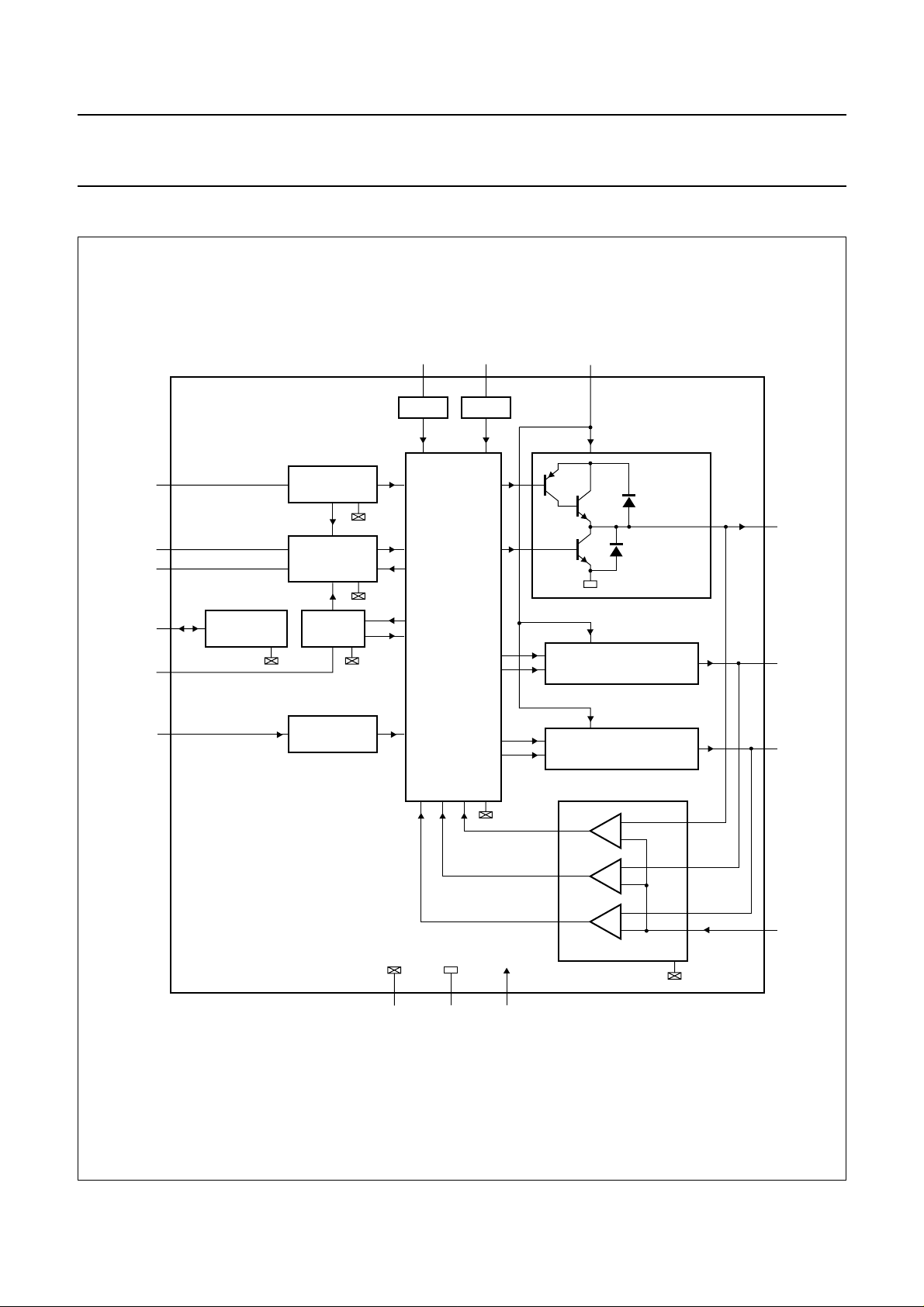
BLOCK DIAGRAM
handbook, full pagewidth
CAP-ST
CAP-DC
CAP-CD
TEST
CAP-TI
DIR
14
13
12
3
15
9
THERMAL
PROTECTION
START-UP
OSCILLATOR
ADAPTIVE
COMMUTATION
DELAY
TIMING
DIRECTION
CONTROL
BRAKE
BRAKE
COMMUTATION
RESET
818
RESET
LOGIC
VMOT
6, 7
PUSH/PULL
FLYBACK
D
H
D
OUTPUT DRIVER
OUTPUT DRIVER
L
STAGE 2
STAGE 3
OUTPUT
DRIVER
STAGE 1
1, 2
4, 5
20,
21
MOT1
MOT2
MOT3
TDA5145TS
10 11
GND2
GND1 V
Fig.1 Block diagram.
1998 Oct 27 3
23, 24
22
MOT0
EMF COMPARATORS
MGR391
P
Page 4
Philips Semiconductors Product specification
Brushless DC motor drive circuit TDA5145TS
PINNING
SYMBOL PIN DESCRIPTION
MOT1 1 driver output 1
MOT1 2 driver output 1
TEST 3 test input/output
MOT2 4 driver output 2
MOT2 5 driver output 2
VMOT 6 input voltage for the output driver
stages
VMOT 7 input voltage for the output driver
stages
BRAKE 8 brake input; this pin may not be left
floating, a LOW-level voltage must
be applied to disable this function
DIR 9 direction control input; this pin may
not be left floating
GND2 10 ground supply return for control
circuits
V
P
11 supply voltage
CAP-CD 12 external capacitor connection for
adaptive communication delay
timing
CAP-DC 13 external capacitor connection for
adaptive communication delay
timing copy
CAP-ST 14 external capacitor connection for
start-up oscillator
CAP-TI 15 external capacitor connection for
timing
n.c. 16 not connected
n.c. 17 not connected
RESET 18 reset input; this pin may not be left
floating, a LOW-level voltage must
be applied to disable this function
n.c. 19 not connected
MOT3 20 driver output 3
MOT3 21 driver output 3
MOT0 22 input from the star point of the motor
coils
GND1 23 ground (0 V) motor supply return for
output stages
GND1 24 ground (0 V) motor supply return for
output stages
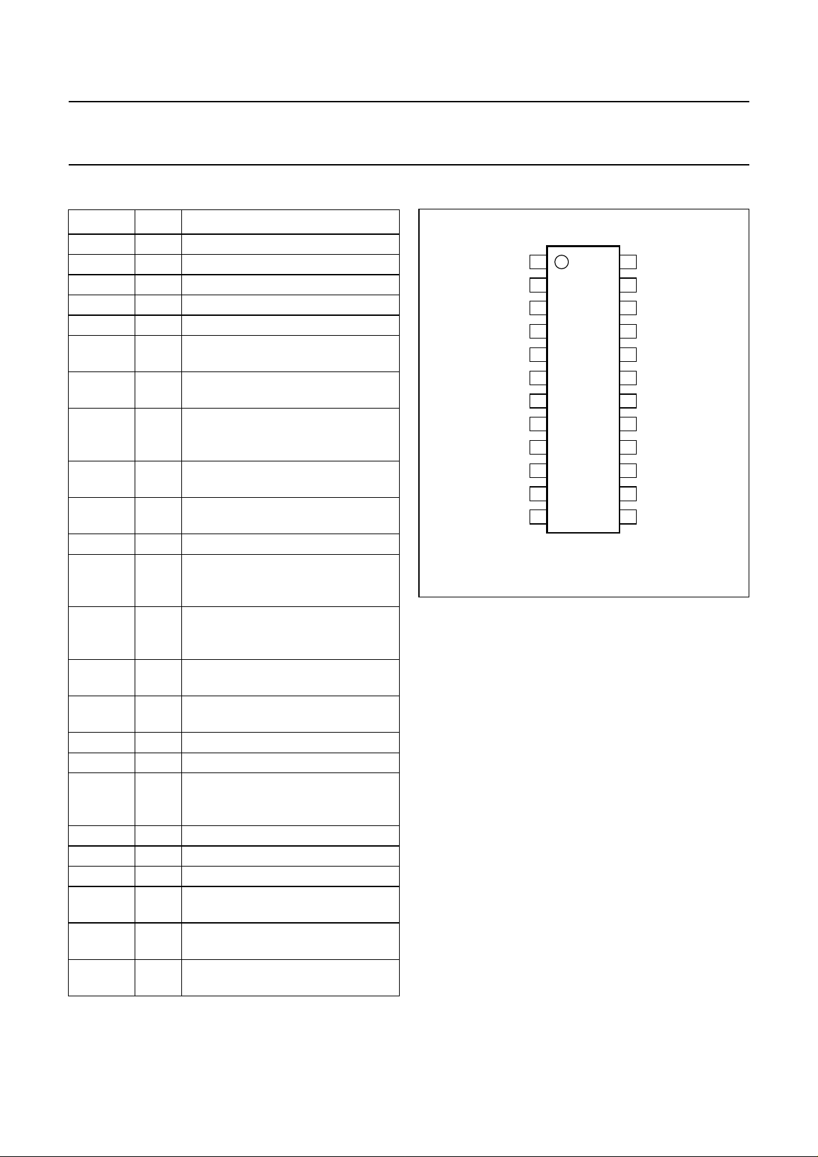
handbook, halfpage
MOT1
MOT1
TEST
MOT2
MOT2
VMOT
VMOT
BRAKE
DIR
GND2
V
CAP-CD
1
2
3
4
5
6
7
8
9
10
11
P
12
TDA5145TS
MGR392
24
23
22
21
20
19
18
17
16
15
14
13
GND1
GND1
MOT0
MOT3
MOT3
n.c.
RESET
n.c.
n.c.
CAP-TI
CAP-ST
CAP-DC
Fig.2 Pin configuration.
FUNCTIONAL DESCRIPTION
The TDA5145TS offers a sensorless 3-phase motor drive
function. It is unique in its combination of sensorless motor
drive and full-wave drive. The TDA5145TS offers
protected outputs capable of handling high currents and
can be used with star or delta connected motors. It can
easily be adapted for different motors and applications.
The TDA5145TS offers the following features:
• Sensorless commutation by using the motor EMF
• Built-in start-up circuit
• Optimum commutation, independent of motor type or
motor loading
• Built-in flyback diodes
• Three phase full-wave drive
• High output current (2.0 A)
• Outputs protected by current limiting and thermal
protection of each output transistor
• Low current consumption by adaptive base-drive
• Soft-switching pulse output for low radiation
• Direction of rotation controlled by one pin
• Brake function.
1998 Oct 27 4
Page 5

Philips Semiconductors Product specification
Brushless DC motor drive circuit TDA5145TS
LIMITING VALUES
In accordance with the Absolute Maximum Rating System (IEC 134).
SYMBOL PARAMETER CONDITIONS MIN. MAX. UNIT
V
P
V
I(n)
V
I(VMOT)
V
O
V
I(n1)
T
stg
T
amb
P
tot
V
es
supply voltage − 18 V
input voltage; all pins except
VI<18V −0.3 VP+ 0.5 V
VMOT
VMOT input voltage −0.5 +17 V
output voltage MOT0, MOT1,
−1V
VMOT+VdFD
V
MOT2 and MOT3
input voltage CAP-ST, CAP-TI,
− 2.5 V
CAP-CD and CAP-DC
storage temperature −55 +150 °C
operating ambient temperature 0 +70 °C
total power dissipation see Fig. 3 −− W
electrostatic handling see Chapter “Handling” − 2000 V
HANDLING
Every pin withstands the ESD test according to
“MIL-STD-883C class 2”
positive and 3 pulses negative on each pin referenced to ground.
1.00
0.57
P
(W)
2
tot
1
0
−50
0 200
50 100 150
70
handbook, halfpage
. Method 3015 (HBM 1500 Ω; 100 pF) 3 pulses
MGL529
T
(°C)
amb
Fig.3 Power derating curve.
1998 Oct 27 5
Page 6

Philips Semiconductors Product specification
Brushless DC motor drive circuit TDA5145TS
CHARACTERISTICS
V
= 14.5 V; T
P
SYMBOL PARAMETER CONDITIONS MIN. TYP. MAX. UNIT
Supply
V
P
I
P
V
i(VMOT)
Thermal protection
T
SD
∆T reduction in temperature before
MOT0; centre tap
V
i
I
bias
V
CSW
∆V
CSW
V
hys
MOT1, MOT2 and MOT3; see Fig.4
V
DO
∆V
sat(lt)
∆V
sat(ut)
I
LIM
t
r
t
f
V
dF(DH)
V
dF(DL)
I
dM
DIR
V
IH
V
IL
I
IL
I
IH
=25°C; unless otherwise specified.
amb
supply voltage note 1 4 − 18 V
supply current note 2 − 6.8 7.8 mA
input voltage to the output driver
see Fig.1 1.7 − 16 V
stages
local temperature at temperature
130 140 150 °C
sensor causing shut-down
after shut-down − T
− 30 − K
SD
switch-on
input voltage −0.5 − V
input bias current 0.5 V < Vi<V
− 1.5 V −10 −−µA
VMOT
VMOT
V
comparator switching level note 3 ±20 ±25 ±30 mV
variation in comparator switching
−− 3mV
levels
comparator input hysteresis − 75 −µV
drop-out output voltage Io= 100 mA − 0.9 1.05 V
I
= 1000 mA − 1.6 1.85 V
o
variation in saturation voltage
Io= 100 mA −− 180 mV
between lower transistors
variation in saturation voltage
Io= −100 mA −− 180 mV
between upper transistors
current limiting V
rise time switching output V
fall time switching output V
diode forward voltage (diode DH)Io=−500 mA;
=10V; Ro= 1.2 Ω 1.8 2.0 2.5 A
VMOT
= 15 V; see Fig.5 5 10 15 µs
VMOT
= 15 V; see Fig.5 10 15 20 µs
VMOT
−− 1.5 V
notes 4 and 5; see Fig.1
diode forward voltage (diode DL)Io= 500 mA;
−1.5 −−V
notes 4 and 5; see Fig.1
peak diode current note 5 −− 2.5 A
HIGH-level input voltage 4V<VP< 18 V 2.0 −−V
LOW-level input voltage 4V<VP<18V −− 0.8 V
LOW-level input current −−20 −µA
HIGH-level input current − 20 −µA
1998 Oct 27 6
Page 7

Philips Semiconductors Product specification
Brushless DC motor drive circuit TDA5145TS
SYMBOL PARAMETER CONDITIONS MIN. TYP. MAX. UNIT
RESET
V
IH
V
IL
I
IL
I
IH
BRAKE
V
IH
V
IL
I
IL
I
IH
CAP-ST
I
o(sink)
I
o(source)
V
swL
V
swH
CAP-TI
I
o(sink)
I
o(source)
V
swL
V
swM
V
swH
CAP-CD
I
o(sink)
I
o(source)
I
sink/Isource
V
IL
V
IH
CAP-DC
I
o(sink)
I
o(source)
I
sink/Isource
V
IL
V
IH
HIGH-level input voltage reset mode;
4V<VP<18V
LOW-level input voltage normal mode;
4V<VP<18V
LOW-level input current Vi= 2.0 V −−20 −µA
HIGH-level input current Vi= 0.8 V − 20 −µA
HIGH-level input voltage brake mode;
4V<VP<18V
LOW-level input voltage normal mode;
4V<VP<18V
LOW-level input current Vi= 2.0 V −−20 −µA
HIGH-level input current Vi= 0.8 V − 20 −µA
output sink current 1.5 2.0 2.5 µA
output source current −2.5 −2.0 −1.5 µA
LOW-level switching voltage − 0.20 − V
HIGH-level switching voltage − 2.20 − V
output sink current − 28 −µA
output source current 0.2 V < V
0.3V<V
< 0.3 V −−57 −µA
CAP-TI
< 2.2 V −−5−µA
CAP-TI
LOW-level switching voltage − 50 − mV
MIDDLE-level switching voltage − 0.30 − V
HIGH-level switching voltage − 2.20 − V
output sink current 10.6 16.2 22 µA
output source current −5.3 −8.1 −11 µA
ratio of sink to source current 1.85 2.05 2.25
LOW-level input voltage 850 875 900 mV
HIGH-level input voltage 2.3 2.4 2.55 V
output sink current 10.1 15.5 20.9 µA
output source current −20.9 −15.5 −10.1 µA
ratio of sink to source current 0.9 1.025 1.15
LOW-level input voltage 850 875 900 mV
HIGH-level input voltage 2.3 2.4 2.55 V
2.0 −−V
−− 0.8 V
2.0 −−V
−− 0.8 V
1998 Oct 27 7
Page 8

Philips Semiconductors Product specification
Brushless DC motor drive circuit TDA5145TS
Notes
1. An unstabilized supply can be used.
2. V
VMOT=VP
3. Switching levels with respect to MOT1, MOT2 and MOT3.
4. Drivers are in the high-impedance OFF-state.
5. The outputs are short-circuit protected by limiting the current and the IC temperature.
, all other inputs at 0 V; all outputs at VP; Io= 0 mA.
handbook, full pagewidth
back EMF signal
V
MOT0
Fig.4 Switching levels with respect to MOT1, MOT2 and MOT3.
handbook, halfpage
V
CSW
12.5 V
hysteresis 75 µV typ.
V
CSW
12.5 V
MGR381
MOT1, MOT2 and MOT3
comparator threshold
voltages
2.0 V
t
r
Fig.5 Output transition time measurement.
1998 Oct 27 8
2.0 V
t
f
MGR382
Page 9

Philips Semiconductors Product specification
Brushless DC motor drive circuit TDA5145TS
APPLICATION INFORMATION
handbook, full pagewidth
GND1
24
23 22 21 20 19 18 17 16 15 14 13
1234567891011
(1) Value selected for 3 Hz start-up oscillator frequency.
Fig.6 Application diagram.
Introduction (see Fig.7)
Full-wave driving of a three phase motor requires three
push-pull output stages. In each of the six possible states
two outputs are active, one sourcing (H) and one sinking
(L). The third output presents a high impedance (Z) to the
motor, which enables measurement of the motor back
EMF in the corresponding motor coil by the EMF
comparator at each output. The commutation logic is
responsible for control of the output transistors and
selection of the correct EMF comparator. The sequence of
the six possible states of the outputs is given in Table 1.
The zero-crossing in the motor EMF (detected by the
comparator selected by the commutation logic) is used to
calculate the correct moment for the next commutation,
that is, the change to the next output state. The delay is
calculated (depending on the motor loading) by the
adaptive commutation delay block.
Because of high inductive loading the output stages
contain flyback diodes. The output stages are also
protected by a current limiting circuit and by thermal
protection of the six output transistors.
(1)
18 nF
220
10
nF
nF
TDA5145TS
12
18 nF
BRAKE DIR
VMOT
10 µF
V
P
MGR393
Table 1 Output states; note 1
STATE MOT1 MOT2 MOT3
1ZLH
2HLZ
3HZL
4ZHL
5LHZ
6LZH
Note
1. H = HIGH state; L = LOW state; Z = high-impedance
OFF-state.
The system will only function when the EMF voltage from
the motor is present. Therefore, a start oscillator is
provided that will generate commutation pulses when no
zero-crossings in the motor voltage are available.
A timing function is incorporated into the device for internal
timing and for timing of the reverse rotation detection.
1998 Oct 27 9
Page 10

Philips Semiconductors Product specification
Brushless DC motor drive circuit TDA5145TS
The TDA5145TS is designed for systems with low current
consumption: use of I2L logic, adaptive base drive for the
output transistors (patented).
Adjustments
The system has been designed in such a way that the
tolerances of the application components are not critical.
However, the approximate values of the following
components must still be determined:
• The start capacitor; this determines the frequency of the
start oscillator.
• The two capacitors in the adaptive commutation delay
circuit; these are important in determining the optimum
moment for commutation, depending on the type and
loading of the motor.
• The timing capacitor; this provides the system with its
timing signals.
HE START CAPACITOR (CAP-ST)
T
This capacitor determines the frequency of the start
oscillator. It is charged and discharged, with a current of
2 µA, from 0.05 to 2.2 V and back to 0.05 V. The time
taken to complete one cycle is given by:
t
= (2.15 × C) s (with C in µF)
start
The start oscillator is reset by a commutation pulse and so
is only active when the system is in the start-up mode.
A pulse from the start oscillator will cause the outputs to
change to the next state (torque in the motor). If the
movement of the motor generates enough EMF the
TDA5145TS will run the motor. If the amount of EMF
generated is insufficient, then the motor will move one step
only and will oscillate in its new position. The amplitude of
the oscillation must decrease sufficiently before the arrival
of the next start pulse, to prevent the pulse arriving during
the wrong phase of the oscillation. The oscillation of the
motor is given by:
f
osc
=
1
---------------------------------- K
I× p×
t
---------------------- -
2π
J
where:
= torque constant (N.m/A)
K
t
I = current (A)
p = number of magnetic pole-pairs
J = inertia J (kg.m2)
If the damping is high then a start frequency of 2 Hz can be
chosen or t = 500 ms, thus C = 0.5/2 = 0.25 µF
(choose 220 nF).
T
HE ADAPTIVE COMMUTATION DELAY (CAP-CD AND
CAP-DC)
In this circuit, capacitor CAP-CD is charged during one
commutation period, with an interruption of the charging
current during the diode pulse. During the next
commutation period this capacitor (CAP-CD) is discharged
at twice the charging current. The charging current is
8.1 µA and the discharging current 16.2 µA; the voltage
range is from 0.9 to 2.2 V. The voltage must stay within
this range at the lowest commutation frequency of
interest, f
==
C
:
C1
×
8.1 10
-------------------------f 1.3×
6–
6231
(C in nF)
------------ f
C1
If the frequency is lower, then a constant commutation
delay after the zero-crossing is generated by the discharge
from 2.2 to 0.9 V at 16.2 µA; maximum
delay = (0.076 × C) ms (with C in nF)
Example: nominal commutation frequency = 900 Hz and
the lowest usable frequency = 400 Hz; thus:
CAP-CD
6231
------------ 400
15.6==
(choose 18 nF)
The other capacitor, CAP-DC, is used to repeat the same
delay by charging and discharging with 15.5 µA. The same
value can be chosen as for CAP-CD. Figure 8 illustrates
typical voltage waveforms.
Example: J = 72 × 10−6kg.m2, Kt=25×10−3N.m/A, p = 6
and I = 0.5 A; this gives f
osc
= 5 Hz.
1998 Oct 27 10
Page 11

Philips Semiconductors Product specification
Brushless DC motor drive circuit TDA5145TS
handbook, full pagewidth
220 nF
18 nF
18 nF
TEST
10 nF
14
13
12
3
PROTECTION
15
10
THERMAL
START-UP
OSCILLATOR
ADAPTIVE
COMMUNICATION
DELAY
TIMING
DIRECTION
CONTROL
BRAKE RESET VMOT
8
BRAKE
COMMUNICATION
18 6, 7 23, 24
RESET
LOGIC
TP
TP
TP
TN
TN
TN
TN
TN
TN
D
D
D
D
D
D
1, 2
4, 5
20, 21
MOTOR
11
V
P
TDA5145TS
GND2
GND1
9
DIR
Fig.7 Typical application of the TDA5145TS as a scanner driver.
1998 Oct 27 11
EMF
COMPARATORS
22
MGR394
Page 12

Philips Semiconductors Product specification
Brushless DC motor drive circuit TDA5145TS
handbook, full pagewidth
voltage
on CAP-CD
voltage
on CAP-DC
Fig.8 CAP-CD and CAP-DC typical voltage waveforms in normal running mode.
THE TIMING CAPACITOR (CAP-TI)
Capacitor CAP-TI is used for timing the successive steps
within one commutation period; these steps include some
internal delays.
The most important function is the watchdog time in which
the motor EMF has to recover from a negative diode pulse
back to a positive EMF voltage (or vice versa). A watchdog
timer is a guarding function that only becomes active when
the expected event does not occur within a predetermined
time.
The EMF usually recovers within a short time if the motor
is running normally (<<ms). However, if the motor is
motionless or rotating in the reverse direction, then the
time can be longer (>>ms).
A watchdog time must be chosen so that it is long enough
for a motor without EMF (still) and eddy currents that may
stretch the voltage in a motor winding; however, it must be
short enough to detect reverse rotation. If the watchdog
time is made too long, then the motor may run in the wrong
direction (with little torque).
t
MGH317
The capacitor is charged with a current of 57 µA, from
0.2 to 0.3 V. Above this level it is charged with a current of
5 µA, up to 2.2 V only if the selected motor EMF remains
in the wrong polarity (watchdog function). At the end, or, if
the motor voltage becomes positive, the capacitor is
discharged with a current of 28 µA. The watchdog time is
the time taken to charge the capacitor with a current of
5 µA, from 0.3 to 2.2 V.
To ensure that the internal delays are covered CAP-TI
must have a minimum value of 2 nF. For the watchdog
function a value of 10 nF for CAP-TI is recommended.
To ensure a good start-up and commutation, care must be
taken that no oscillations occur at the trailing edge of the
flyback pulse. Snubber networks at the outputs should be
critically damped.
Typical voltage waveforms are illustrated in Fig.9.
1998 Oct 27 12
Page 13

Philips Semiconductors Product specification
Brushless DC motor drive circuit TDA5145TS
handbook, full pagewidth
V
MOT 1
voltage
on CAP-TI
MGH318
If the chosen value of CAP-TI is too small oscillations can occur in certain positions of a blocked rotor. If the chosen value is too large, then it is possible
that the motor may run in the reverse direction (synchronously with little torque).
Fig.9 Typical CAP-TI and V
voltage waveforms in normal running mode.
MOT1
Other design aspects
There are other design aspects concerning the application
of the TDA5145TS besides the commutation function.
They are:
• Direction function
• Brake function
• Reliability.
D
IRECTION FUNCTION
If the voltage at pin 9 is less than 0.8 V, the motor is
running in one direction (depending on the motor
connections). If the voltage at pin 9 is greater than 2.0 V,
the motor is running in the opposite direction.
BRAKE
FUNCTION
If the voltage at pin 8 is greater than 2.0 V, the motor
brakes. In that condition, the 3 outputs MOT1, MOT2 and
MOT3 are forced to a LOW voltage level and the current
limitation is performed internally by the sink drivers.
RESET
FUNCTION
If the voltage at pin 18 is greater than 2.0 V, the output
states are shown in Table 2.
Table 2 Output states if V
DRIVER OUTPUT STATE
RESET
> 2.0 V
(1)
MOT1 Z
MOT2 L
MOT3 H
Note
1. Z = high-impedance OFF-state; L = LOW state;
H = HIGH state.
1998 Oct 27 13
Page 14

Philips Semiconductors Product specification
Brushless DC motor drive circuit TDA5145TS
Table 3 Switching sequence after a reset pulse; note 1
DIR RESET MOT1 MOT2 DIR FUNCTION
H H Z L H reset
H L Z L H normal direction
HLHLZ
HLHZL
HLZHL
HLLHZ
HLLZH
L H H L Z reset
L L H L Z reverse direction
LLZLH
LLLZH
LLLHZ
LLZHL
LLHZL
mode sequence
mode sequence
Note
1. Z = high-impedance OFF-state; L = LOW state; H = HIGH state.
Table 4 Priority of function; note 1
BRAKE TEST RESET FUNCTION
L L L normal
L L H reset
L H L test
L H H test
H L L brake
H L H brake
H H L brake
H H H brake
Note
1. L = LOW state; H = HIGH state.
R
ELIABILITY
It is necessary to protect high current circuits and the output stages are protected in two ways:
• Current limiting of the ‘lower’ output transistors. The ‘upper’ output transistors use the same base current as the
conducting ‘lower’ transistor (+15%). This means that the current to and from the output stages is limited.
• Thermal protection of the six output transistors is achieved by each transistor having a thermal sensor that is active
when the transistor is switched on. The transistors are switched off when the ambient temperature becomes too high.
1998 Oct 27 14
Page 15

Philips Semiconductors Product specification
Brushless DC motor drive circuit TDA5145TS
PACKAGE OUTLINE
SSOP24: plastic shrink small outline package; 24 leads; body width 5.3 mm
D
c
y
Z
24 13
A
2
A
pin 1 index
1
SOT340-1
E
H
E
Q
L
p
L
(A )
A
X
v M
A
A
3
θ
112
w M
b
e
DIMENSIONS (mm are the original dimensions)
UNIT A1A2A
Note
1. Plastic or metal protrusions of 0.20 mm maximum per side are not included.
A
max.
0.21
mm
2.0
OUTLINE
VERSION
SOT340-1 MO-150AG
0.05
1.80
1.65
IEC JEDEC EIAJ
0.25
b
3
p
0.38
0.25
p
cD
0.20
8.4
0.09
8.0
REFERENCES
0 2.5 5 mm
scale
(1)E(1) (1)
5.4
0.65 1.25
5.2
1998 Oct 27 15
detail X
eHELLpQZywv θ
7.9
7.6
1.03
0.63
0.9
0.7
EUROPEAN
PROJECTION
0.13 0.10.2
0.8
0.4
ISSUE DATE
93-09-08
95-02-04
o
8
o
0
Page 16

Philips Semiconductors Product specification
Brushless DC motor drive circuit TDA5145TS
SOLDERING
Introduction
There is no soldering method that is ideal for all IC
packages. Wave soldering is often preferred when
through-hole and surface mounted components are mixed
on one printed-circuit board. However, wave soldering is
not always suitable for surface mounted ICs, or for
printed-circuits with high population densities. In these
situations reflow soldering is often used.
This text gives a very brief insight to a complex technology.
A more in-depth account of soldering ICs can be found in
our
“Data Handbook IC26; Integrated Circuit Packages”
(order code 9398 652 90011).
Reflow soldering
Reflow soldering techniques are suitable for all SSOP
packages.
Reflow soldering requires solder paste (a suspension of
fine solder particles, flux and binding agent) to be applied
to the printed-circuit board by screen printing, stencilling or
pressure-syringe dispensing before package placement.
Several techniques exist for reflowing; for example,
thermal conduction by heated belt. Dwell times vary
between 50 and 300 seconds depending on heating
method. Typical reflow temperatures range from
215 to 250 °C.
Preheating is necessary to dry the paste and evaporate
the binding agent. Preheating duration: 45 minutes at
45 °C.
Wave soldering
Wave soldering is not recommended for SSOP packages.
This is because of the likelihood of solder bridging due to
closely-spaced leads and the possibility of incomplete
solder penetration in multi-lead devices.
If wave soldering cannot be avoided, the following
conditions must be observed:
• A double-wave (a turbulent wave with high upward
pressure followed by a smooth laminar wave)
soldering technique should be used.
• The longitudinal axis of the package footprint must
be parallel to the solder flow and must incorporate
solder thieves at the downstream end.
Even with these conditions, only consider wave
soldering SSOP packages that have a body width of
4.4 mm, that is SSOP16 (SOT369-1) or
SSOP20 (SOT266-1).
During placement and before soldering, the package must
be fixed with a droplet of adhesive. The adhesive can be
applied by screen printing, pin transfer or syringe
dispensing. The package can be soldered after the
adhesive is cured.
Maximum permissible solder temperature is 260 °C, and
maximum duration of package immersion in solder is
10 seconds, if cooled to less than 150 °C within
6 seconds. Typical dwell time is 4 seconds at 250 °C.
A mildly-activated flux will eliminate the need for removal
of corrosive residues in most applications.
Repairing soldered joints
Fix the component by first soldering two diagonallyopposite end leads. Use only a low voltage soldering iron
(less than 24 V) applied to the flat part of the lead. Contact
time must be limited to 10 seconds at up to 300 °C. When
using a dedicated tool, all other leads can be soldered in
one operation within 2 to 5 seconds between
270 and 320 °C.
1998 Oct 27 16
Page 17

Philips Semiconductors Product specification
Brushless DC motor drive circuit TDA5145TS
DEFINITIONS
Data sheet status
Objective specification This data sheet contains target or goal specifications for product development.
Preliminary specification This data sheet contains preliminary data; supplementary data may be published later.
Product specification This data sheet contains final product specifications.
Limiting values
Limiting values given are in accordance with the Absolute Maximum Rating System (IEC 134). Stress above one or
more of the limiting values may cause permanent damage to the device. These are stress ratings only and operation
of the device at these or at any other conditions above those given in the Characteristics sections of the specification
is not implied. Exposure to limiting values for extended periods may affect device reliability.
Application information
Where application information is given, it is advisory and does not form part of the specification.
LIFE SUPPORT APPLICATIONS
These products are not designed for use in life support appliances, devices, or systems where malfunction of these
products can reasonably be expected to result in personal injury. Philips customers using or selling these products for
use in such applications do so at their own risk and agree to fully indemnify Philips for any damages resulting from such
improper use or sale.
1998 Oct 27 17
Page 18

Philips Semiconductors Product specification
Brushless DC motor drive circuit TDA5145TS
NOTES
1998 Oct 27 18
Page 19

Philips Semiconductors Product specification
Brushless DC motor drive circuit TDA5145TS
NOTES
1998 Oct 27 19
Page 20

Philips Semiconductors – a worldwide company
Argentina: see South America
Australia: 34 Waterloo Road, NORTH RYDE, NSW 2113,
Tel. +61 2 9805 4455, Fax. +61 2 9805 4466
Austria: Computerstr. 6, A-1101 WIEN, P.O. Box 213, Tel. +43 160 1010,
Fax. +43 160 101 1210
Belarus: Hotel Minsk Business Center, Bld. 3, r. 1211, Volodarski Str. 6,
220050 MINSK, Tel. +375 172 200 733, Fax. +375 172 200 773
Belgium: see The Netherlands
Brazil: seeSouth America
Bulgaria: Philips Bulgaria Ltd., Energoproject, 15thfloor,
51 James Bourchier Blvd., 1407 SOFIA,
Tel. +359 2 689 211, Fax. +359 2 689 102
Canada: PHILIPS SEMICONDUCTORS/COMPONENTS,
Tel. +1 800 234 7381
China/Hong Kong: 501 Hong Kong Industrial Technology Centre,
72 Tat Chee Avenue, Kowloon Tong, HONG KONG,
Tel. +852 2319 7888, Fax. +852 2319 7700
Colombia: see South America
Czech Republic: see Austria
Denmark: Prags Boulevard 80, PB 1919, DK-2300 COPENHAGEN S,
Tel. +45 32 88 2636, Fax. +45 31 57 0044
Finland: Sinikalliontie 3, FIN-02630 ESPOO,
Tel. +358 9 615800, Fax. +358 9 61580920
France: 51 Rue Carnot, BP317, 92156 SURESNES Cedex,
Tel. +33 1 40 99 6161, Fax. +33 1 40 99 6427
Germany: Hammerbrookstraße 69, D-20097 HAMBURG,
Tel. +49 40 23 53 60, Fax. +49 40 23 536 300
Greece: No. 15, 25th March Street, GR 17778 TAVROS/ATHENS,
Tel. +30 1 4894 339/239, Fax. +30 1 4814 240
Hungary: seeAustria
India: Philips INDIA Ltd, Band Box Building, 2nd floor,
254-D, Dr. Annie Besant Road, Worli, MUMBAI 400 025,
Tel. +91 22 493 8541, Fax. +91 22 493 0966
Indonesia: PT Philips Development Corporation, Semiconductors Division,
Gedung Philips, Jl. Buncit Raya Kav.99-100, JAKARTA 12510,
Tel. +62 21 794 0040 ext. 2501, Fax. +62 21 794 0080
Ireland: Newstead, Clonskeagh, DUBLIN 14,
Tel. +353 1 7640 000, Fax. +353 1 7640 200
Israel: RAPAC Electronics, 7 Kehilat Saloniki St, PO Box 18053,
TEL AVIV 61180, Tel. +972 3 645 0444, Fax. +972 3 649 1007
Italy: PHILIPS SEMICONDUCTORS, Piazza IV Novembre 3,
20124 MILANO, Tel. +39 2 6752 2531, Fax. +39 2 6752 2557
Japan: Philips Bldg 13-37, Kohnan 2-chome, Minato-ku,
TOKYO 108-8507, Tel. +81 3 3740 5130, Fax. +81 3 3740 5077
Korea: Philips House, 260-199 Itaewon-dong, Yongsan-ku, SEOUL,
Tel. +82 2 709 1412, Fax. +82 2 709 1415
Malaysia: No. 76 Jalan Universiti, 46200 PETALING JAYA, SELANGOR,
Tel. +60 3 750 5214, Fax. +60 3 757 4880
Mexico: 5900 Gateway East, Suite 200, EL PASO, TEXAS 79905,
Tel. +9-5 800 234 7381
Middle East: see Italy
Netherlands: Postbus 90050, 5600PB EINDHOVEN, Bldg. VB,
Tel. +31 40 27 82785, Fax. +31 40 27 88399
New Zealand: 2 Wagener Place, C.P.O. Box 1041, AUCKLAND,
Tel. +64 9 849 4160, Fax. +64 9 849 7811
Norway: Box 1, Manglerud 0612, OSLO,
Tel. +47 22 74 8000, Fax. +47 22 74 8341
Pakistan: see Singapore
Philippines: Philips Semiconductors Philippines Inc.,
106 Valero St. Salcedo Village, P.O. Box 2108 MCC, MAKATI,
Metro MANILA, Tel. +63 2 816 6380, Fax. +63 2 817 3474
Poland: Ul. Lukiska 10, PL 04-123 WARSZAWA,
Tel. +48 22 612 2831, Fax. +48 22 612 2327
Portugal: see Spain
Romania: see Italy
Russia: Philips Russia, Ul. Usatcheva 35A, 119048 MOSCOW,
Tel. +7 095 755 6918, Fax. +7 095 755 6919
Singapore: Lorong 1, Toa Payoh, SINGAPORE 319762,
Tel. +65 350 2538, Fax. +65 251 6500
Slovakia: see Austria
Slovenia: see Italy
South Africa: S.A. PHILIPS Pty Ltd., 195-215 Main Road Martindale,
2092 JOHANNESBURG, P.O. Box 7430 Johannesburg 2000,
Tel. +27 11 470 5911, Fax. +27 11 470 5494
South America: Al. Vicente Pinzon, 173, 6th floor,
04547-130 SÃO PAULO, SP, Brazil,
Tel. +55 11 821 2333, Fax. +55 11 821 2382
Spain: Balmes 22, 08007 BARCELONA,
Tel. +34 93 301 6312, Fax. +34 93 301 4107
Sweden: Kottbygatan 7, Akalla, S-16485 STOCKHOLM,
Tel. +46 8 5985 2000, Fax. +46 8 5985 2745
Switzerland: Allmendstrasse 140, CH-8027 ZÜRICH,
Tel. +41 1 488 2741 Fax. +41 1 488 3263
Taiwan: Philips Semiconductors, 6F, No. 96, Chien Kuo N. Rd., Sec. 1,
TAIPEI, Taiwan Tel. +886 2 2134 2865, Fax. +886 2 2134 2874
Thailand: PHILIPS ELECTRONICS (THAILAND) Ltd.,
209/2 Sanpavuth-Bangna Road Prakanong, BANGKOK 10260,
Tel. +66 2 745 4090, Fax. +66 2 398 0793
Turkey: Talatpasa Cad. No. 5, 80640 GÜLTEPE/ISTANBUL,
Tel. +90 212 279 2770, Fax. +90 212 282 6707
Ukraine: PHILIPS UKRAINE, 4 Patrice Lumumba str., Building B, Floor 7,
252042 KIEV, Tel. +380 44 264 2776, Fax. +380 44 268 0461
United Kingdom: Philips Semiconductors Ltd., 276 Bath Road, Hayes,
MIDDLESEX UB3 5BX, Tel. +44 181 730 5000, Fax. +44 181 754 8421
United States: 811 East Arques Avenue, SUNNYVALE, CA 94088-3409,
Tel. +1 800 234 7381
Uruguay: see South America
Vietnam: see Singapore
Yugoslavia: PHILIPS, Trg N. Pasica 5/v, 11000 BEOGRAD,
Tel. +381 11 625 344, Fax.+381 11 635 777
For all other countries apply to: Philips Semiconductors,
International Marketing & Sales Communications, Building BE-p, P.O. Box 218,
5600 MD EINDHOVEN, The Netherlands, Fax. +31 40 27 24825
© Philips Electronics N.V. 1998 SCA60
All rights are reserved. Reproduction in whole or in part is prohibited without the prior written consent of the copyright owner.
The information presented in this document does not form part of any quotation or contract, is believed to be accurate and reliable and may be changed
without notice. No liability will be accepted by the publisher for any consequence of its use. Publication thereof does not convey nor imply any license
under patent- or other industrial or intellectual property rights.
Internet: http://www.semiconductors.philips.com
Printed in The Netherlands 295102/750/01/pp20 Date of release: 1998 Oct 27 Document order number: 9397 750 04042
 Loading...