

Page 1

INTEGRATED CIRCUITS
DATA SH EET
TDA5051A
Home automation modem
Product specification
Supersedes data of 1997 Sep 19
File under Integrated Circuits, IC11
1999 May 31
Page 2

Philips Semiconductors Product specification
Home automation modem TDA5051A
FEATURES
• Full digital carrier generation and shaping
• Modulation/demodulation frequency set by clock
adjustment, from microcontroller or on-chip oscillator
• High clock rate of 6-bit A/D (Digital to Analog) converter
for rejection of aliasing components
APPLICATIONS
• Home appliance control (air conditioning, shutters,
lighting, alarms and so on)
• Energy/heating control
• Amplitude Shift Keying (ASK) data transmission using
the home power network.
• Fully integrated output power stage with overload
protection
• Automatic Gain Control (AGC) at receiver input
• 8-bit A/D (Analog to Analog) converter and narrow
digital filtering
• Digital demodulation delivering baseband data
GENERAL DESCRIPTION
The TDA5051A is a modem IC, specifically dedicated to
ASK transmission by means of the home power supply
network, at 600 or 1200 baud data rate. It operates from a
single 5 V supply.
• Easy compliance with EN50065-1 with simple coupling
network
• Few external components for low cost applications
• SO16 plastic package.
QUICK REFERENCE DATA
SYMBOL PARAMETER CONDITIONS MIN. TYP. MAX. UNIT
V
DD
I
DD(tot)
supply voltage 4.75 5.0 5.25 V
total supply current f
= 8.48 MHz
osc
reception mode − 28 38 mA
transmission mode (
DATAIN=0) ZL=30Ω−47 68 mA
power-down mode − 19 25 mA
f
cr
f
osc
V
o(rms)
carrier frequency note 1 95 132.5 148.5 kHz
oscillator frequency 6.08 8.48 9.504 MHz
output carrier signal on CISPR16 load
120 − 122 dBµV
(RMS value)
V
i(rms)
THD total harmonic distortion on CISPR16
input signal (RMS value) note 2 82 − 122 dBµV
−−55 − dB
load with coupling network
Z
L
load impedance 1 30 −Ω
BR baud rate − 600 1200 bits/s
T
amb
ambient temperature 0 − 70 °C
Notes
1. Frequency range corresponding to the EN50065-1 band. However, the modem can operate at any lower oscillator
frequency.
2. The minimum value can be improved by using an external amplifier, see application diagrams Figs 22 and 23.
1999 May 31 2
Page 3
Philips Semiconductors Product specification
Home automation modem TDA5051A
ORDERING INFORMATION
TYPE
NUMBER
NAME DESCRIPTION VERSION
PACKAGE
TDA5051AT SO16 plastic small outline package; 16 leads; body width 7.5 mm SOT162-1
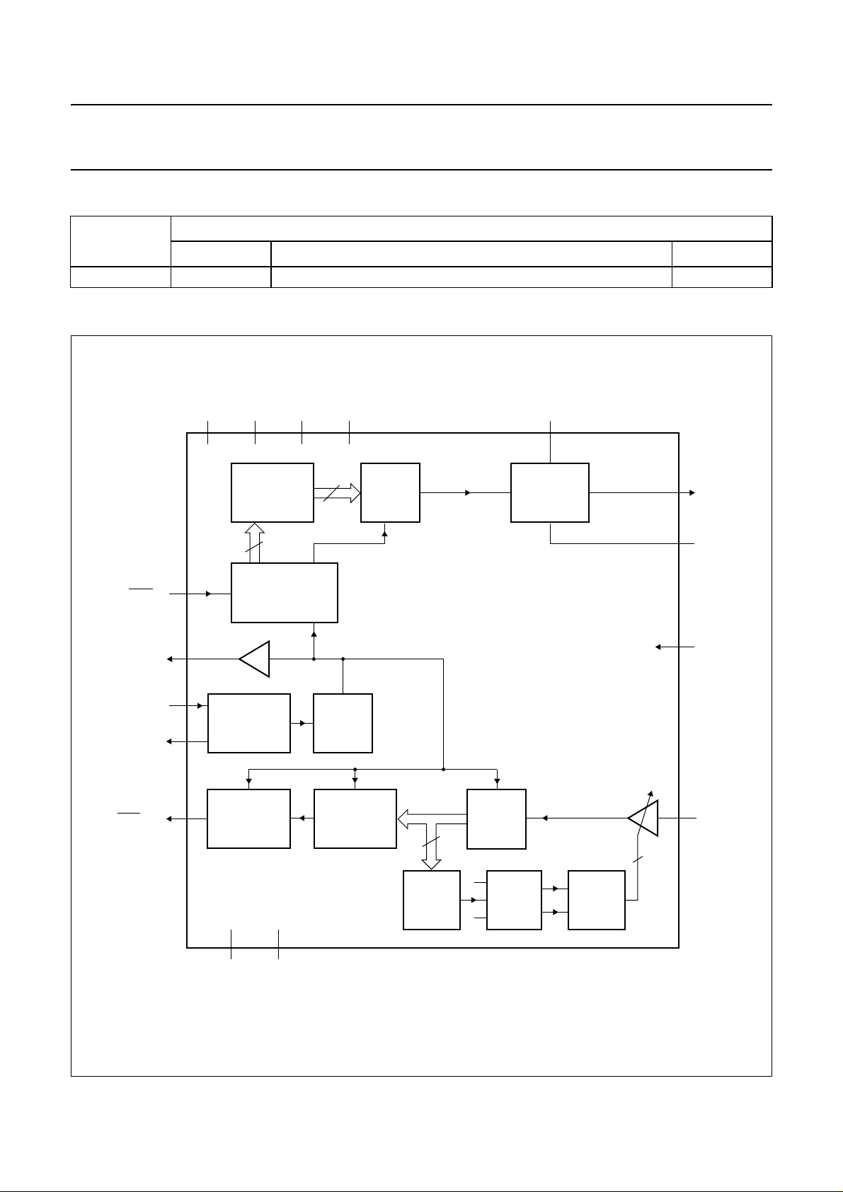
BLOCK DIAGRAM
handbook, full pagewidth
DATA
IN
CLK
OUT
DGND
1
4
AGND12V
5
CONTROL LOGIC
ROM
10
DDA
13
V
DDD
311
modulated
6
DAC clock
D/A
filter clock
carrier
V
DDAP
POWER
DRIVE
WITH
PROTECTION
TDA5051A
10
9
15
TX
OUT
APGND
PD
7
OSCILLATOR
8
2
DIGITAL
DEMODULATOR
16
TEST1 SCANTEST
2
÷
DIGITAL
BAND-PASS
FILTER
DETECT
6
DATA
OSC1
OSC2
OUT
Fig.1 Block diagram.
1999 May 31 3
PEAK
14
A/D
8
H
L
U
D
COUNT
5
U/D
MGK832
RX
IN
Page 4

Philips Semiconductors Product specification
Home automation modem TDA5051A
PINNING
SYMBOL PIN DESCRIPTION
DATA
IN
DATA
OUT
V
DDD
CLK
OUT
DGND 5 digital ground
SCANTEST 6 test input (LOW in application)
OSC1 7 oscillator input
OSC2 8 oscillator output
APGND 9 analog ground for power amplifier
TX
OUT
V
DDAP
AGND 12 analog ground
V
DDA
RX
IN
PD 15 power-down input (active HIGH)
TEST1 16 test input (HIGH in application)
1 digital data input (active LOW)
2 digital data output (active LOW)
3 digital supply voltage
4 clock output
10 analog signal output
11 analog supply voltage for power
amplifier
13 analog supply voltage
14 analog signal input
handbook, halfpage
DATA
SCANTEST
DATA
CLK
OUT
V
DDD
OUT
DGND
OSC1
OSC2
IN
1
2
3
4
TDA5051AT
5
6
7
8
Fig.2 Pin configuration.
MGK833
16
15
14
13
12
11
10
9
TEST1
PD
RX
IN
V
DDA
AGND
V
DDAP
TX
OUT
APGND
FUNCTIONAL DESCRIPTION
Both transmission and reception stages are controlled
either by the master clock of the microcontroller or by the
on-chip reference oscillator connected to a crystal. This
ensures the accuracy of the transmission carrier and the
exact trimming of the digital filter, thus making the
performance totally independent of application
disturbances such as component spread, temperature,
supply drift and so on.
The interface with the power network is made by means of
an LC network (see Fig.18). The device includes a power
output stage that feeds a 120 dBµV (RMS) signal on a
typical 30 Ω load.
To reduce power consumption, the IC is disabled by a
power-down input (pin PD): in this mode, the on-chip
oscillator remains active and the clock continues to be
supplied at pin CLK
. For low-power operation in
OUT
reception mode, this pin can be dynamically controlled by
the microcontroller, see Section “Power-down mode”.
When the circuit is connected to an external clock
generator (see Fig.6), the clock signal must be applied at
pin OSC1 (pin 7); OSC2 (pin 8) must be left open-circuit.
Fig.7 shows the use of the on-chip clock circuit.
All logic inputs and outputs are compatible with
TTL/CMOS levels, providing an easy connection to a
standard microcontroller I/O port.
The digital part of the IC is fully scan-testable. Two digital
inputs, SCANTEST and TEST1, are used for production
test: these pins must be left open-circuit in functional mode
(correct levels are internally defined by pull-up or
pull-down resistors).
Transmission mode
To provide strict stability with respect to environmental
conditions, the carrier frequency is generated by scanning
the ROM memory under the control of the microcontroller
clock or the reference frequency provided by the on-chip
oscillator. High frequency clocking rejects the aliasing
components to such an extent that they are filtered by the
coupling LC network and do not cause any significant
disturbance. The data modulation is applied through
pin DATAIN and smoothly applied by specific digital circuits
to the carrier (shaping). Harmonic components are limited
in this process, thus avoiding unacceptable disturbance of
the transmission channel (according to CISPR16 and
EN50065-1 recommendations). A −55 dB Total Harmonic
Distortion (TDH) is reached when the typical LC coupling
network (or an equivalent filter) is used.
1999 May 31 4
Page 5

Philips Semiconductors Product specification
Home automation modem TDA5051A
The DAC and the power stage are set in order to provide
a maximum signal level of 122 dBµV (RMS) at the output.
The output of the power stage (TX
) must always be
OUT
connected to a decoupling capacitor, because of a DC
level of 0.5VDD at this pin, which is present even when the
device is not transmitting. This pin must also be protected
against overvoltage and negative transient signals.
The DC level of TX
can be used to bias a unipolar
OUT
transient suppressor, as shown in the application diagram;
see Fig.18.
Direct connection to the mains is done through an LC
network for low-cost applications. However, a HF signal
transformer could be used when power-line insulation has
to be performed.
CAUTION
In transmission mode, the receiving part of the circuit is
not disabled and the detection of the transmitted signal
is normally performed. In this mode, the gain chosen
before the beginning of the transmission is stored, and
the AGC is internally set to −6dB as long as DATA
IN
is LOW. Then, the old gain setting is automatically
restored.
Reception mode
After digital demodulation, the baseband data signal is
made available after pulse shaping.
The signal pin (RXIN) is a high-impedance input which has
to be protected and DC decoupled for the same reasons
as with pin TX
. The high sensitivity (82 dBµV) of this
OUT
input requires an efficient 50 Hz rejection filter (realized by
the LC coupling network), which also acts as an
anti-aliasing filter for the internal digital processing;
see Fig.18.
Data format
T
RANSMISSION MODE
The data input (DATAIN) is active LOW: this means that a
burst is generated on the line (pin TX
) when DATA
OUT
IN
pin is LOW.
Pin TX
is in a high-impedance state as long as the
OUT
device is not transmitting. Successive logic 1s are treated
in a Non-Return-to-Zero (NRZ) mode, see pulse shapes in
Figs 8 and 9.
R
ECEPTION MODE
The data output (pin DATA
) is active LOW; this means
OUT
that the data output is LOW when a burst is received.
Pin DATA
remains LOW as long as a burst is received.
OUT
The input signal received by the modem is applied to a
wide range input amplifier with AGC (−6 to +30 dB). This is
basically for noise performance improvement and signal
level adjustment, which ensures a maximum sensitivity of
the ADC. An 8-bit conversion is then performed, followed
Power-down mode
Power-down input (pin PD) is active HIGH; this means that
the power consumption is minimum when pin PD is HIGH.
Now, all functions are disabled, except clock generation.
by digital band-pass filtering, to meet the CISPR
normalization and to comply with some additional
limitations met in current applications.
LIMITING VALUES
In accordance with the Absolute Maximum Rating System (IEC 134).
SYMBOL PARAMETER MIN. MAX. UNIT
V
f
T
T
T
DD
osc
stg
amb
j
supply voltage 4.5 5.5 V
oscillator frequency − 12 MHz
storage temperature −50 +150 °C
ambient temperature −10 +80 °C
junction temperature − 125 °C
HANDLING
Inputs and outputs are protected against electrostatic discharge in normal handling. However, to be totally safe, it is
desirable to take normal precautions appropriate to handling MOS devices.
1999 May 31 5
Page 6

Philips Semiconductors Product specification
Home automation modem TDA5051A
CHARACTERISTICS
V
DDD=VDDA
SYMBOL PARAMETER CONDITIONS MIN. TYP. MAX. UNIT
Supply
V
DD
I
DD(RX/TX)(tot)
I
DD(PD)(tot)
I
DD(PAMP)
I
DD(PAMP)(max)
=5V±5%; T
= 0 to 70 °C; V
amb
connected to V
DDD
; DGND connected to AGND.
DDA
supply voltage 4.75 5 5.25 V
total analog + digital
supply current
total analog + digital
supply current;
VDD=5V±5%
TX or RX mode
VDD=5V±5%;
PD = HIGH
− 28 38 mA
− 19 25 mA
Power-down mode
power amplifier supply
current
VDD=5V±5%;
ZL=30Ω;
− 19 30 mA
DATAIN= LOW
in transmission mode
maximum power amplifier
supply current
VDD=5V±5%;
ZL=1Ω;
− 76 − mA
DATAIN= LOW
in transmission mode
DATAIN and PD inputs: DATA
V
IH
V
IL
V
OH
V
OL
HIGH-level input voltage 0.2VDD+ 0.9 − VDD+ 0.5 V
LOW-level input voltage −0.5 − 0.2VDD− 0.1 V
HIGH-level output voltage IOH= −1.6 mA 2.4 −− V
LOW-level output voltage IOL= 1.6 mA −−0.45 V
and CLK
OUT
OUT
outputs
OSC1 input and OSC2 output (OSC2 only used for driving external quartz crystal; must be left open-circuit
when using an external clock generator)
V
IH
V
IL
V
OH
V
OL
HIGH-level input voltage 0.7V
DD
− VDD+ 0.5 V
LOW-level input voltage −0.5 − 0.2VDD− 0.1 V
HIGH-level output voltage IOH= −1.6 mA 2.4 −− V
LOW-level output voltage IOL= 1.6 mA −−0.45 V
Clock
f
osc
f
osc
-------f
cr
f
osc
---------------------
f
CLKOUT
oscillator frequency 6.080 − 9.504 MHz
ratio between oscillator
− 64 −
and carrier frequency
ratio between oscillator
− 2 −
and clock output frequency
Transmission mode
f
cr
t
su
t
h
carrier frequency f
set-up time of the shaped
burst
hold time of the shaped
burst
= 8.48 MHz − 132.5 − kHz
osc
f
= 8.48 MHz;
osc
− 170 −µs
see Fig.8
f
= 8.48 MHz;
osc
− 170 −µs
see Fig.8
1999 May 31 6
Page 7

Philips Semiconductors Product specification
Home automation modem TDA5051A
SYMBOL PARAMETER CONDITIONS MIN. TYP. MAX. UNIT
t
W(DI)(min)
V
o(rms)
I
o(max)
Z
o
V
O
THD total harmonic distortion on
B
−20dB
minimum pulse width of
DATAIN signal
output carrier signal
(RMS value)
power amplifier maximum
output current (peak value)
output impedance of the
power amplifier
output DC level at
pin TX
OUT
CISPR16 load with the
coupling network
(measured on the first ten
harmonics)
bandwidth of the shaped
output signal (at −20 dB)
on CISPR16 load with the
coupling network
f
= 8.48 MHz;
osc
see Fig.8
ZL= CISPR16;
DATAIN= LOW
ZL=1Ω;
DATAIN= LOW
V
= 121 dBµV on
o(rms)
CISPR16 load;
f
= 8.48 MHz;
osc
DATAIN= LOW
(no modulation);
see Figs 3 and 16
V
= 121 dBµV on
o(rms)
CISPR16 load;
f
= 8.48 MHz;
osc
DATAIN= 300 Hz;
duty factor = 50%;
see Fig.4
− 190 −µs
120 − 122 dBµV
− 160 − mA
− 5 −Ω
− 2.5 − V
−−55 − dB
− 3000 − Hz
Reception mode
V
i(rms)
analog input signal
(RMS value)
V
I
Z
i
R
AGC
t
c(AGC)
t
d(dem)(su)
DC level at pin RX
IN
RXIN input impedance − 50 − kΩ
AGC range − 36 − dB
AGC time constant f
demodulation delay set-up
time
t
d(dem)(h)
demodulation delay hold
time
B
det
detection bandwidth f
BER bit error rate f
82 − 122 dBµV
− 2.5 − V
= 8.48 MHz;
osc
− 296 −µs
see Fig.5
f
= 8.48 MHz;
osc
− 350 400 µs
see Fig.15
f
= 8.48 MHz;
osc
− 420 470 µs
see Fig.15
= 8.48 MHz − 3 − kHz
osc
= 8.48 MHz;
osc
− 1 − 1 × 10
600 baud; S/N = 35 dB;
signal 76 dBµV;
see Fig.17
−4
1999 May 31 7
Page 8

Philips Semiconductors Product specification
Home automation modem TDA5051A
SYMBOL PARAMETER CONDITIONS MIN. TYP. MAX. UNIT
Power-up timing
t
d(pu)(TX)
delay between power-up
and DATAIN in
transmission mode
t
d(pu)(RX)
delay between power-up
and DATA
mode
Power-down timing
t
d(pd)(TX)
delay between PD = 0 and
DA TAIN in transmission
mode
t
d(pd)(RX)
delay between PD = 0 and
DA TA
mode
t
active(min)
minimum active time with
T = 10 ms power-down
period in reception mode
OUT
in reception
OUT
in reception
XTAL = 8.48 MHz;
C1 = C2 = 27 pF;
Rp= 2.2 MΩ; see Fig.10
XTAL = 8.48 MHz;
C1 = C2 = 27 pF;
Rp= 2.2 MΩ;
f
= 132.5 kHz;
RXIN
120 dBµV sine wave;
see Fig.11
f
= 8.48 MHz;
osc
see Fig.12
f
= 8.48 MHz;
osc
f
= 132.5 kHz;
RXIN
120 dBµV sine wave;
see Fig.13
f
= 8.48 MHz;
osc
f
= 132.5 kHz;
RXIN
120 dBµV sine wave;
see Fig.14
− 1 −µs
− 1 −µs
− 10 −µs
− 500 −µs
− 1 −µs
book, full pagewidth
0
V
o(rms)
(dBV)
−100
5
10
Resolution bandwidth =9 kHz; top: 0 dBV (RMS) = 120 dBµV (RMS); marker at −5 dBV (RMS) = 115 dBµV (RMS);
the CISPR16 network provides an attenuation of 6 dB, so the signal amplitude is 121 dBµV (RMS).
132.5 kHz
Fig.3 Carrier spectrum.
f (Hz)
MGK834
6
10
1999 May 31 8
Page 9

Philips Semiconductors Product specification
Home automation modem TDA5051A
handbook, full pagewidth
−10
dBV
(RMS)
−60
117.5 132.5
Resolution bandwidth = 100 Hz; B
= 3000 Hz (2 × 1500 Hz).
−20dB
1500 Hz
20 dB
Fig.4 Shaped signal spectrum.
f (kHz)
MBH664
147.5
handbook, full pagewidth
V
RXIN
V
G
AGC
+30 dB
−6 dB
(I)
0
(AGC time constant)
modulated sine wave 122 dBµV amplitude
t
c(AGC)
Fig.5 AGC time constant definition (not to scale).
1999 May 31 9
t
8.68 dB
AGC range
MGK011
Page 10

Philips Semiconductors Product specification
Home automation modem TDA5051A
TIMING
Configuration for clock
handbook, full pagewidth
For parameter description, see Table 1.
XTAL
CLK
OUT
MICRO-
CONTROLLER
GND
Fig.6 External clock.
f
osc
OSC1
DGND
7
TDA5051A
5
MGK835
handbook, full pagewidth
MICRO-
CONTROLLER
For parameter description, see Table 1.
CLK
GND
IN
CLK
OUT
1
/2 f
osc
4
TDA5051A R
DGND
5
Fig.7 Typical configuration for on-chip clock circuit.
1999 May 31 10
8
7
OSC2
OSC1
C1
p
XTAL
C2
MGK836
Page 11

Philips Semiconductors Product specification
Home automation modem TDA5051A
Table 1 Clock oscillator parameters
OSCILLATOR
FREQUENCY
f
osc
CARRIER FREQUENCY
f
cr
CLOCK OUTPUT
FREQUENCY
1
⁄2f
osc
EXTERNAL COMPONENTS
6.080 to 9.504 MHz 95 to 148.5 kHz 3.040 to 4.752 MHz C1 = C2 = 27 to 47 pF;
= 2.2 to 4.7 MΩ;
R
p
XTAL = standard quartz crystal
Table 2 Calculation of parameters depending on the clock frequency
SYMBOL PARAMETER CONDITIONS UNIT
f
osc
oscillator frequency with on-chip oscillator: frequency of the crystal
Hz
quartz; with external clock: frequency of the
signal applied at OSC1
f
CLKOUT
f
cr
clock output frequency
carrier frequency/digital filter tuning
1
1
⁄2f
⁄64f
osc
osc
Hz
Hz
frequency
t
su
t
h
t
W(DI)(min)
t
W(burst)(min)
t
c(AGC)
t
su(demod)
t
h(demod)
set-up time of the shaped burst
hold time of the shaped burst
minimum pulse width of DATAIN signal
minimum burst time of V
signal t
O(DC)
AGC time constant s
demodulation set-up time
demodulation hold time
23
1472
or
------
------------ -
f
23
-----f
t
2514
------------ -
3200
------------ -
3800
------------ -
f
cr
osc
1472
or
------------ f
cr
osc
1
+
-----
su
f
cr
W(DI)(min)+th
f
osc
(≈max.)
f
osc
(≈max.)
f
osc
s
s
s
s
s
s
1999 May 31 11
Page 12

Philips Semiconductors Product specification
Home automation modem TDA5051A
handbook, full pagewidth
(1) t
W(DI)>tW(DI)(min)
(2) t
W(DI)(min)=tsu
(3) t
W(DI)(min)<tsu
+
; wrong operation.
TX
OUT
V
O(DC)
t
su
0
t
DATA
IN
.
1
----f
cr
W(DI)
Fig.8 Relationship between DATAIN and TX
Table 3 Relationship between DATAIN and TX
t
W(burst)
t
(1) (2) (3)
OUT
t
W(burst)(min)
h
t
W(DI)(min)
(see Table 3).
OUT
MGK837
Note
1. X = don’t care.
PD
1X
DATA
(1)
IN
TX
OUT
high-impedance
0 1 high-impedance (after t
0 0 active with DC offset
handbook, halfpage
100%
t
W(burst)
t
su
t
h
MGK010
Fig.9 Pulse shape characteristics.
)
h
1999 May 31 12
Page 13

Philips Semiconductors Product specification
Home automation modem TDA5051A
Timing diagrams
OUT
OUT
90% V
DD
NOT DEFINED CLOCK STABLE
t
d(pu)(TX)
HIGH
IN
handbook, full pagewidth
DATAIN is an edge-sensitive input and must be HIGH before starting a transmission.
V
DD
CLK
DATA
TX
Fig.10 Timing diagram during power-up in transmission mode.
MGK015
OUT
OUT
90% V
DD
NOT DEFINED
NOT DEFINED
t
d(pu)(RX)
HIGH
handbook, full pagewidth
V
DD
CLK
RX
DATA
IN
Fig.11 Timing diagram during power-up in reception mode.
1999 May 31 13
CLOCK STABLE
t
d(dem)(h)
MGK016
Page 14

Philips Semiconductors Product specification
Home automation modem TDA5051A
handbook, full pagewidth
handbook, full pagewidth
PD
DATA
TX
PD
RX
DATA
OUT
IN
OUT
IN
t
d(pd)(TX)
normal operation wrong operation
TX
OUT
delayed by PD
MGK017
Fig.12 Power-down sequence in transmission mode.
handbook, full pagewidth
PD
RX
DATA
I
DD
IN
OUT
I
I
0
DD(RX)
DD(PD)
t
d(dem)(su)
DATA
delayed by PD
OUT
t
d(pd)(RX)
Fig.13 Power-down sequence in reception mode.
t
active(min)
T
Fig.14 Power saving by dynamic control of power-down.
t
d(pd)(RX)
MGK018
MGK845
1999 May 31 14
Page 15

Philips Semiconductors Product specification
Home automation modem TDA5051A
TEST INFORMATION
handbook, full pagewidth
pulse
generator
300 Hz
50%
DATA
TX
OUT
DATA
IN
/RX
OUT
OSCILLOSCOPE
IN
DATA
Y1
t
d(dem)(su)
DATA
OUT
Y2
OUT
1 µF
IN
1
TX
10
TDA5051A
(to be tested)
2
78
t
d(dem)(h)
XTAL
f
osc
14
RX
10 nF
IN
30 Ω
MGK838
Fig.15 Test set-up for measuring demodulation delay.
1999 May 31 15
Page 16

Philips Semiconductors Product specification
Home automation modem TDA5051A
handbook, full pagewidth
OSC1
OSC2
7
TDA5051A
8
1 13, 3, 11
DATA
IN
(2)(1)
TX
OUT
10
AGND, DGND, APGND
12, 5, 9
V
DDA, VDDD, VDDAP
+5 V
POWER
SUPPLY
10 µF
33 nF
coupling
network
47 µH
(3)
33 nF
47 µH
CISPR16
network
250 nF
50 µH
5 Ω
250 nF
50 µH
5 Ω
(4)
50 Ω
SPECTRUM
ANALYSER
50 Ω
MGK839
(1) Square wave TTL signal 300 Hz, duty factor = 50% for measuring signal bandwidth (see spectrum Fig.3).
(2) DATAIN= LOW for measuring total harmonic distortion (see spectrum Fig.3).
(3) Tuned for fcr= 132.5 kHz.
(4) The CISPR16 network provides a −6 dB attenuation.
Fig.16 Test set-up for measuring THD and bandwidth of the TX
1999 May 31 16
OUT
signal.
Page 17

Philips Semiconductors Product specification
Home automation modem TDA5051A
handbook, full pagewidth
DATA
TDA5051A
1
IN
78
OSC1 OSC2
XTAL = 8.48 MHz
OSC1 OSC2
78
TDA5051A
(to be tested)
2
DATA
OUT
TX
OUT
10
AGND, DGND, APGND
12,
5,
9
RX
IN
14
12,
AGND, DGND, APGND
5,
9
DATA
DATA
in
out
IN
OUT
COUPLING
NETWORK
(1)
WHITE
NOISE
GENERATOR
COUPLING
NETWORK
(1)
V24/TTL
INTERFACE
out
out
in
+
+
PARAMETERS
PSEUDO RANDOM SEQUENCE:
RXD
TXD
9
2
−1 BITS LONG
V24 SERIAL DATA
ANALYSER
SPECTRUM
ANALYSER
50 Ω
600 BAUD
(1) See Fig.16.
Fig.17 Test set-up for measuring Bit Error Rate (BER).
1999 May 31 17
MGK840
Page 18

Philips Semiconductors Product specification
Home automation modem TDA5051A
APPLICATION INFORMATION
handbook, full pagewidth
+5 V
250 V (AC)
max
MICRO-
CONTROLLER
+5 V
DATA
DATA
CLK
78L05
47 nF
OUT
OUT
PD
2
IN
T 630 mA
31
1
2
4
15
7
470 µF
(16 V)
OSC1
2.2 MΩ
MOV
250 V (AC)
1N4006
7V5
(1.3 W)
100 µF
(16 V)
V
DDDVDDAP
3
TDA5051A
859 12
OSC2
APGND AGNDDGND
250 V (AC)
68 Ω
(2 W)
1 mH
1N4006
V
DDA
1311
14
10
2 µF
RX
TX
IN
OUT
10 nF
47 nF
(63 V)
47 µH
SA5.0A
47 nF/X2
250 V (AC)
47 µH
low R
S
1 µF
(16 V)
XTAL
7.3728 MHz
fcr= 115.2 kHz for a XTAL = 7.3728 MHz standard crystal.
Fig.18 Application diagram without power line insulation.
1999 May 31 18
27 pF27 pF
MGK841
Page 19

Philips Semiconductors Product specification
Home automation modem TDA5051A
20
handbook, full pagewidth
gain
(dB)
0
−
20
−
40
−
60
−
80
−
100
10
Main features of the coupling network: 50 Hz rejection >80 dB; anti-aliasing for the digital filter >50 dB at the
sampling frequency (
2
10
1
⁄2f
). Input impedance always higher than 10 Ω within the 95 to 148.5 kHz band.
osc
1
2
3
10
4
10
5
10
6
10
f (Hz)
Fig.19 Gain (curve 1) and input impedance (curve 2) of the coupling network (fcr= 115.2 kHz; L = 47 µH;
C = 47 nF).
MBH907
3
10
impedance
2
10
10
7
10
input
(Ω)
130
handbook, halfpage
V
o
(dBµV)
120
110
100
110
Fig.20 Output voltage as a function of line impedance (with coupling network; L = 47 µH; C = 47 nF).
1999 May 31 19
MBH908
2
Z
(Ω)
line
10
Page 20

Philips Semiconductors Product specification
Home automation modem TDA5051A
handbook, full pagewidth
+5 V
250 V (AC)
max
MICRO-
CONTROLLER
+5 V
DATA
DATA
CLK
47 nF
OUT
OUT
PD
78L05
2
IN
1
2
4
15
T 630 mA
31
470 µF
(16 V)
7
OSC1
2.2 MΩ
MOV
250 V (AC)
1 VA
FDB08
100 µF
(16 V)
V
DDDVDDAPVDDA
3
TDA5051A
859 12
OSC2
APGND AGNDDGND
100 Ω
(0.5 W)
230 V
6 V
1311
470 nF/X2
250 V (AC)
47 µH
low R
NEWPORT
76250
26
15
100 Ω
100 nF
(63 V)
22 µH
RX
14
TX
OUT
10
10 nF
IN
SA5.0A
S
1 µF
(16 V)
XTAL
7.3728 MHz
27 pF27 pF
fcr= 115.2 kHz for a XTAL = 7.3728 MHz standard crystal.
Fig.21 Application diagram with power line insulation.
1999 May 31 20
MGK842
Page 21

Philips Semiconductors Product specification
Home automation modem TDA5051A
handbook, full pagewidth
+5 V
CONTROLLER
250 V (AC)
MICRO-
max
+5 V
DATA
DATA
CLK
78L05
47 nF
OUT
OUT
PD
2
IN
T 630 mA
1
2
4
15
7
31
470 µF
(16 V)
OSC1
100 µF
2.2 MΩ
MOV
250 V (AC)
1N4006
7V5
(1.3 W)
(16 V)
V
DDDVDDAP
3
TDA5051A
859 12
OSC2
APGND AGNDDGND
250 V (AC)
68 Ω
(2 W)
1 mH
1N4006
V
DDA
1311
14
10
2 µF
RX
TX
IN
OUT
10 nF
BC547B
47 nF/X2
250 V (AC)
10
kΩ
1 kΩ
47 µH
low R
47 nF
(63 V)
47 µH
150
kΩ
10 nF
33
kΩ
S
1 µF
(16 V)
XTAL
7.3728 MHz
27 pF27 pF
fcr= 115.2 kHz for a XTAL = 7.3728 MHz standard crystal.
Fig.22 Application diagram without power line insulation, with improved sensitivity (68 dBµV typ.).
1999 May 31 21
SA5.0A
MGK843
Page 22

Philips Semiconductors Product specification
Home automation modem TDA5051A
handbook, full pagewidth
+5 V
250 V (AC)
max
MICRO-
CONTROLLER
+5 V
DATA
DATA
CLK
47 nF
OUT
OUT
PD
78L05
2
IN
1
2
4
15
T 630 mA
31
470 µF
(16 V)
7
OSC1
2.2 MΩ
MOV
250 V (AC)
1 VA
FDB08
100 µF
(16 V)
V
DDDVDDAPVDDA
3
TDA5051A
859 12
OSC2
APGND AGNDDGND
100 Ω
(0.5 W)
230 V
6 V
1311
470 nF/X2
250 V (AC)
47 µH
low R
NEWPORT
76250
26
15
100 Ω
100 nF
(63 V)
22 µH
10
kΩ
1 kΩ
150
kΩ
33
kΩ
10 nF
10 nF
RX
IN
14
BC547B
TX
OUT
10
S
1 µF
(16 V)
XTAL
7.3728 MHz
27 pF27 pF
fcr= 115.2 kHz for a XTAL = 7.3728 MHz standard crystal.
Fig.23 Application diagram with power line insulation, with improved sensitivity (68 dBµV typ.).
1999 May 31 22
SA5.0A
MGK844
Page 23

Philips Semiconductors Product specification
Home automation modem TDA5051A
PACKAGE OUTLINE
SO16: plastic small outline package; 16 leads; body width 7.5 mm
D
c
y
Z
16
pin 1 index
1
e
9
A
2
A
8
w M
b
p
SOT162-1
E
H
E
Q
1
L
p
L
detail X
(A )
A
X
v M
A
A
3
θ
0 5 10 mm
scale
DIMENSIONS (inch dimensions are derived from the original mm dimensions)
mm
OUTLINE
VERSION
SOT162-1
A
max.
2.65
0.10
A
1
0.30
0.10
0.012
0.004
A2A
2.45
2.25
0.096
0.089
IEC JEDEC EIAJ
075E03 MS-013AA
0.25
0.01
b
3
p
0.49
0.32
0.36
0.23
0.019
0.013
0.014
0.009
UNIT
inches
Note
1. Plastic or metal protrusions of 0.15 mm maximum per side are not included.
(1)E(1) (1)
cD
10.5
7.6
7.4
0.30
0.29
1.27
0.050
10.1
0.41
0.40
REFERENCES
1999 May 31 23
eHELLpQ
10.65
10.00
0.419
0.394
1.4
0.055
1.1
0.4
0.043
0.016
1.1
1.0
0.043
0.039
PROJECTION
0.25
0.25 0.1
0.01
0.01
EUROPEAN
ywv θ
Z
0.9
0.4
0.035
0.004
0.016
ISSUE DATE
95-01-24
97-05-22
o
8
o
0
Page 24

Philips Semiconductors Product specification
Home automation modem TDA5051A
SOLDERING
Introduction to soldering surface mount packages
This text gives a very brief insight to a complex technology.
A more in-depth account of soldering ICs can be found in
our
“Data Handbook IC26; Integrated Circuit Packages”
(document order number 9398 652 90011).
There is no soldering method that is ideal for all surface
mount IC packages. Wave soldering is not always suitable
for surface mount ICs, or for printed-circuit boards with
high population densities. In these situations reflow
soldering is often used.
Reflow soldering
Reflow soldering requires solder paste (a suspension of
fine solder particles, flux and binding agent) to be applied
to the printed-circuit board by screen printing, stencilling or
pressure-syringe dispensing before package placement.
Several methods exist for reflowing; for example,
infrared/convection heating in a conveyor type oven.
Throughput times (preheating, soldering and cooling) vary
between 100 and 200 seconds depending on heating
method.
Typical reflow peak temperatures range from
215 to 250 °C. The top-surface temperature of the
packages should preferable be kept below 230 °C.
Wave soldering
Conventional single wave soldering is not recommended
for surface mount devices (SMDs) or printed-circuit boards
with a high component density, as solder bridging and
non-wetting can present major problems.
To overcome these problems the double-wave soldering
method was specifically developed.
If wave soldering is used the following conditions must be
observed for optimal results:
• Use a double-wave soldering method comprising a
turbulent wave with high upward pressure followed by a
smooth laminar wave.
• For packages with leads on two sides and a pitch (e):
– larger than or equal to 1.27 mm, the footprint
longitudinal axis is preferred to be parallel to the
transport direction of the printed-circuit board;
– smaller than 1.27 mm, the footprint longitudinal axis
must be parallel to the transport direction of the
printed-circuit board.
The footprint must incorporate solder thieves at the
downstream end.
• For packages with leads on four sides, the footprint must
be placed at a 45° angle to the transport direction of the
printed-circuit board. The footprint must incorporate
solder thieves downstream and at the side corners.
During placement and before soldering, the package must
be fixed with a droplet of adhesive. The adhesive can be
applied by screen printing, pin transfer or syringe
dispensing. The package can be soldered after the
adhesive is cured.
Typical dwell time is 4 seconds at 250 °C.
A mildly-activated flux will eliminate the need for removal
of corrosive residues in most applications.
Manual soldering
Fix the component by first soldering two
diagonally-opposite end leads. Use a low voltage (24 V or
less) soldering iron applied to the flat part of the lead.
Contact time must be limited to 10 seconds at up to
300 °C.
When using a dedicated tool, all other leads can be
soldered in one operation within 2 to 5 seconds between
270 and 320 °C.
1999 May 31 24
Page 25

Philips Semiconductors Product specification
Home automation modem TDA5051A
Suitability of surface mount IC packages for wave and reflow soldering methods
PACKAGE
WAVE REFLOW
(1)
BGA, SQFP not suitable suitable
SOLDERING METHOD
HLQFP, HSQFP, HSOP, HTSSOP, SMS not suitable
(3)
PLCC
, SO, SOJ suitable suitable
LQFP, QFP, TQFP not recommended
SSOP, TSSOP, VSO not recommended
(2)
(3)(4)
(5)
suitable
suitable
suitable
Notes
1. All surface mount (SMD) packages are moisture sensitive. Depending upon the moisture content, the maximum
temperature (with respect to time) and body size of the package, there is a risk that internal or external package
cracks may occur due to vaporization of the moisture in them (the so called popcorn effect). For details, refer to the
Drypack information in the
“Data Handbook IC26; Integrated Circuit Packages; Section: Packing Methods”
.
2. These packages are not suitable for wave soldering as a solder joint between the printed-circuit board and heatsink
(at bottom version) can not be achieved, and as solder may stick to the heatsink (on top version).
3. If wave soldering is considered, then the package must be placed at a 45° angle to the solder wave direction.
The package footprint must incorporate solder thieves downstream and at the side corners.
4. Wave soldering is only suitable for LQFP, TQFP and QFP packages with a pitch (e) equal to or larger than 0.8 mm;
it is definitely not suitable for packages with a pitch (e) equal to or smaller than 0.65 mm.
5. Wave soldering is only suitable for SSOP and TSSOP packages with a pitch (e) equal to or larger than 0.65 mm; it is
definitely not suitable for packages with a pitch (e) equal to or smaller than 0.5 mm.
DEFINITIONS
Data sheet status
Objective specification This data sheet contains target or goal specifications for product development.
Preliminary specification This data sheet contains preliminary data; supplementary data may be published later.
Product specification This data sheet contains final product specifications.
Limiting values
Limiting values given are in accordance with the Absolute Maximum Rating System (IEC 134). Stress above one or
more of the limiting values may cause permanent damage to the device. These are stress ratings only and operation
of the device at these or at any other conditions above those given in the Characteristics sections of the specification
is not implied. Exposure to limiting values for extended periods may affect device reliability.
Application information
Where application information is given, it is advisory and does not form part of the specification.
LIFE SUPPORT APPLICATIONS
These products are not designed for use in life support appliances, devices, or systems where malfunction of these
products can reasonably be expected to result in personal injury. Philips customers using or selling these products for
use in such applications do so at their own risk and agree to fully indemnify Philips for any damages resulting from such
improper use or sale.
1999 May 31 25
Page 26

Philips Semiconductors Product specification
Home automation modem TDA5051A
NOTES
1999 May 31 26
Page 27

Philips Semiconductors Product specification
Home automation modem TDA5051A
NOTES
1999 May 31 27
Page 28

Philips Semiconductors – a worldwide company
Argentina: see South America
Australia: 34 Waterloo Road, NORTH RYDE, NSW 2113,
Tel. +61 2 9805 4455, Fax. +61 2 9805 4466
Austria: Computerstr. 6, A-1101 WIEN, P.O. Box 213,
Tel. +43 1 60 101 1248, Fax. +43 1 60 101 1210
Belarus: Hotel Minsk Business Center, Bld. 3, r. 1211, Volodarski Str. 6,
220050 MINSK, Tel. +375 172 20 0733, Fax. +375 172 20 0773
Belgium: see The Netherlands
Brazil: seeSouth America
Bulgaria: Philips Bulgaria Ltd., Energoproject, 15thfloor,
51 James Bourchier Blvd., 1407 SOFIA,
Tel. +359 2 68 9211, Fax. +359 2 68 9102
Canada: PHILIPS SEMICONDUCTORS/COMPONENTS,
Tel. +1 800 234 7381, Fax. +1 800 943 0087
China/Hong Kong: 501 Hong Kong Industrial Technology Centre,
72 Tat Chee Avenue, Kowloon Tong, HONG KONG,
Tel. +852 2319 7888, Fax. +852 2319 7700
Colombia: see South America
Czech Republic: see Austria
Denmark: Sydhavnsgade 23, 1780 COPENHAGEN V,
Tel. +45 33 29 3333, Fax. +45 33 29 3905
Finland: Sinikalliontie 3, FIN-02630 ESPOO,
Tel. +358 9 615 800, Fax. +358 9 6158 0920
France: 51 Rue Carnot, BP317, 92156 SURESNES Cedex,
Tel. +33 1 4099 6161, Fax. +33 1 4099 6427
Germany: Hammerbrookstraße 69, D-20097 HAMBURG,
Tel. +49 40 2353 60, Fax. +49 40 2353 6300
Hungary: seeAustria
India: Philips INDIA Ltd, Band Box Building, 2nd floor,
254-D, Dr. Annie Besant Road, Worli, MUMBAI 400 025,
Tel. +91 22 493 8541, Fax. +91 22 493 0966
Indonesia: PT Philips Development Corporation, Semiconductors Division,
Gedung Philips, Jl. Buncit Raya Kav.99-100, JAKARTA 12510,
Tel. +62 21 794 0040 ext. 2501, Fax. +62 21 794 0080
Ireland: Newstead, Clonskeagh, DUBLIN 14,
Tel. +353 1 7640 000, Fax. +353 1 7640 200
Israel: RAPAC Electronics, 7 Kehilat Saloniki St, PO Box 18053,
TEL AVIV 61180, Tel. +972 3 645 0444, Fax. +972 3 649 1007
Italy: PHILIPS SEMICONDUCTORS, Piazza IV Novembre 3,
20124 MILANO, Tel. +39 02 67 52 2531, Fax. +39 02 67 52 2557
Japan: Philips Bldg 13-37, Kohnan 2-chome, Minato-ku,
TOKYO 108-8507, Tel. +81 3 3740 5130, Fax. +81 3 3740 5057
Korea: Philips House, 260-199 Itaewon-dong, Yongsan-ku, SEOUL,
Tel. +82 2 709 1412, Fax. +82 2 709 1415
Malaysia: No. 76 Jalan Universiti, 46200 PETALING JAYA, SELANGOR,
Tel. +60 3 750 5214, Fax. +60 3 757 4880
Mexico: 5900 Gateway East, Suite 200, EL PASO, TEXAS 79905,
Tel. +9-5 800 234 7381, Fax +9-5 800 943 0087
Middle East: see Italy
Netherlands: Postbus 90050, 5600 PB EINDHOVEN, Bldg. VB,
Tel. +31 40 27 82785, Fax. +31 40 27 88399
New Zealand: 2 Wagener Place, C.P.O. Box 1041, AUCKLAND,
Tel. +64 9 849 4160, Fax. +64 9 849 7811
Norway: Box 1, Manglerud 0612, OSLO,
Tel. +47 22 74 8000, Fax. +47 22 74 8341
Pakistan: see Singapore
Philippines: Philips Semiconductors Philippines Inc.,
106 Valero St. Salcedo Village, P.O. Box 2108 MCC, MAKATI,
Metro MANILA, Tel. +63 2 816 6380, Fax. +63 2 817 3474
Poland: Ul. Lukiska 10, PL 04-123 WARSZAWA,
Tel. +48 22 612 2831, Fax. +48 22 612 2327
Portugal: see Spain
Romania: see Italy
Russia: Philips Russia, Ul. Usatcheva 35A, 119048 MOSCOW,
Tel. +7 095 755 6918, Fax. +7 095 755 6919
Singapore: Lorong 1, Toa Payoh, SINGAPORE 319762,
Tel. +65 350 2538, Fax. +65 251 6500
Slovakia: see Austria
Slovenia: see Italy
South Africa: S.A. PHILIPS Pty Ltd., 195-215 Main Road Martindale,
2092 JOHANNESBURG, P.O. Box 58088 Newville 2114,
Tel. +27 11 471 5401, Fax. +27 11 471 5398
South America: Al. Vicente Pinzon, 173, 6th floor,
04547-130 SÃO PAULO, SP, Brazil,
Tel. +55 11 821 2333, Fax. +55 11 821 2382
Spain: Balmes 22, 08007 BARCELONA,
Tel. +34 93 301 6312, Fax. +34 93 301 4107
Sweden: Kottbygatan 7, Akalla, S-16485 STOCKHOLM,
Tel. +46 8 5985 2000, Fax. +46 8 5985 2745
Switzerland: Allmendstrasse 140, CH-8027 ZÜRICH,
Tel. +41 1 488 2741 Fax. +41 1 488 3263
Taiwan: Philips Semiconductors, 6F, No. 96, Chien Kuo N. Rd., Sec. 1,
TAIPEI, Taiwan Tel. +886 2 2134 2886, Fax. +886 2 2134 2874
Thailand: PHILIPS ELECTRONICS (THAILAND) Ltd.,
209/2 Sanpavuth-Bangna Road Prakanong, BANGKOK 10260,
Tel. +66 2 745 4090, Fax. +66 2 398 0793
Turkey: Yukari Dudullu, Org. San. Blg., 2.Cad. Nr. 28 81260 Umraniye,
ISTANBUL, Tel. +90 216 522 1500, Fax. +90 216 522 1813
Ukraine: PHILIPS UKRAINE, 4 Patrice Lumumba str., Building B, Floor 7,
252042 KIEV, Tel. +380 44 264 2776, Fax. +380 44 268 0461
United Kingdom: Philips Semiconductors Ltd., 276 Bath Road, Hayes,
MIDDLESEX UB3 5BX, Tel. +44 181 730 5000, Fax. +44 181 754 8421
United States: 811 East Arques Avenue, SUNNYVALE, CA 94088-3409,
Tel. +1 800 234 7381, Fax. +1 800 943 0087
Uruguay: see South America
Vietnam: see Singapore
Yugoslavia: PHILIPS, Trg N. Pasica 5/v, 11000 BEOGRAD,
Tel. +381 11 62 5344, Fax.+381 11 63 5777
For all other countries apply to: Philips Semiconductors,
International Marketing & Sales Communications, Building BE-p, P.O. Box 218,
5600 MD EINDHOVEN, The Netherlands, Fax. +31 40 27 24825
© Philips Electronics N.V. SCA
All rights are reserved. Reproduction in whole or in part is prohibited without the prior written consent of the copyright owner.
The information presented in this document does not form part of any quotation or contract, is believed to be accurate and reliable and may be changed
without notice. No liability will be accepted by the publisher for any consequence of its use. Publication thereof does not convey nor imply any license
under patent- or other industrial or intellectual property rights.
1999 65
Internet: http://www.semiconductors.philips.com
Printed in The Netherlands 295002/25/02/pp28 Date of release: 1999 May 31 Document order number: 9397750 05035
 Loading...