

Page 1

INTEGRATED CIRCUITS
DATA SH EET
TDA4887PS
160 MHz bus-controlled monitor
video preamplifier
Product specification
File under Integrated Circuits, IC02
2001 Oct 19
Page 2

Philips Semiconductors Product specification
160 MHz bus-controlled monitor video
preamplifier
CONTENTS
1 FEATURES
2 GENERAL DESCRIPTION
3 ORDERING INFORMATION
4 QUICK REFERENCE DATA
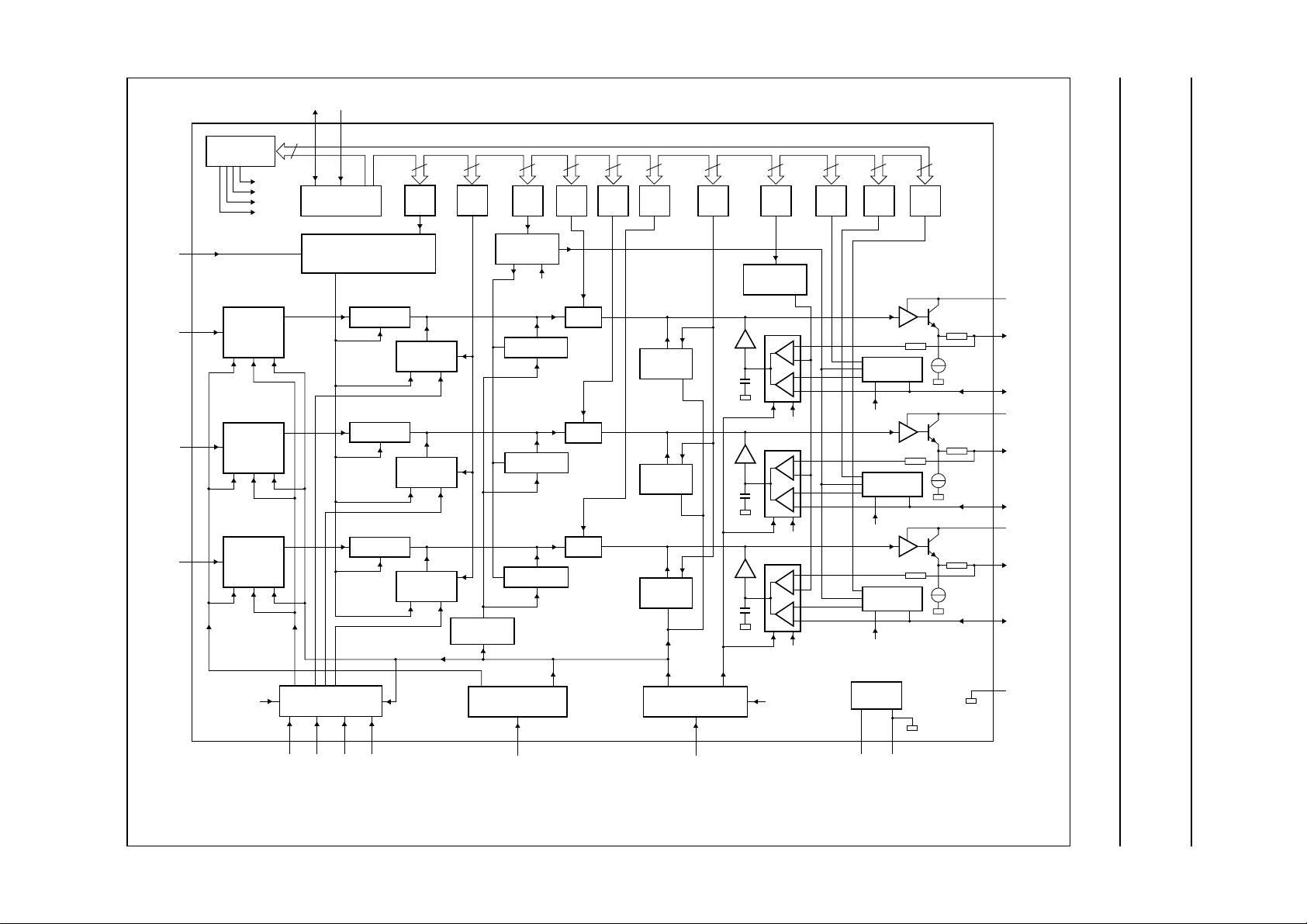
5 BLOCK DIAGRAM
6 PINNING
7 FUNCTIONAL DESCRIPTION
7.1 Signal input stage
7.2 Electronic potentiometer stages
7.3 Output stage
7.4 Pedestal blanking
7.5 Output clamping and feedback references
7.6 Clamping and blanking pulses
7.7 On Screen Display insertion and OSD contrast
7.8 Subcontrast adjustment, contrast modulation
and beam current limiting
7.9 I2C-bus control
7.10 I2C-bus data buffer
8 LIMITING VALUES
9 THERMAL CHARACTERISTICS
TDA4887PS
10 CHARACTERISTICS
11 I2C-BUS PROTOCOL
12 TEST AND APPLICATION INFORMATION
12.1 Test board
12.2 Application boardwith monolithic post amplifier
12.3 Building the application board
12.4 Application hints
13 INTERNAL CIRCUITRY
14 PACKAGE OUTLINE
15 SOLDERING
15.1 Introduction to soldering through-hole mount
packages
15.2 Soldering by dipping or by solder wave
15.3 Manual soldering
15.4 Suitability of through-hole mount IC packages
for dipping and wave soldering methods
16 DATA SHEET STATUS
17 DEFINITIONS
18 DISCLAIMERS
19 PURCHASE OF PHILIPS I2C COMPONENTS
2001 Oct 19 2
Page 3

Philips Semiconductors Product specification
160 MHz bus-controlled monitor video
preamplifier
1 FEATURES
• 160 MHz pixel rate
• 2.7 ns rise time, 3.6 ns fall time
• I2C-bus control
• I2C-bus data buffer for synchronization of adjustments
• 8-bit Digital-to-Analog Converters (DACs)
• 200 ns input clamping pulse
• 4.6 V (p-p) output signal
• Brightness control with grey scale tracking for
user-friendly performance (4 dB more than TDA4885
and TDA4886)
• Brightness control without grey scale tracking for easy
alignment
• On Screen Display (OSD) mixing with 50 MHz pixel rate
• OSD contrast
• Negative feedback for DC-coupled cathodes
• Especially for AC-coupled cathodes
– Bus controlled black level adaptable to post amplifier
type
– Internal positive feedback
– DAC outputs for black level restoration
• Integrated black level storage capacitors
• Beam current limiting
• Subcontrast/contrast modulation
• Adjustable pedestal blanking
• Sync clipping.
TDA4887PS
2 GENERAL DESCRIPTION
The TDA4887PS is a monolithic integrated RGB
preamplifier for colour monitor systems (e.g. 15" and 17")
with I2C-bus control and OSD. In addition to bus control,
beam current limiting and contrast modulation are
possible. The IC offers brightness control with or without
grey scale tracking for easy alignment. The signals are
amplified to drive commonly used video modules or
discrete solutions. A choice can be made between
individual black level control with negative feedback from
the cathode (DC coupling), or black level control with
positive feedback and three DAC outputs for external
cut-off control (AC coupling).
The circuit can be used with special advantages in
conjunction with the TDA485x monitor deflection IC family.
3 ORDERING INFORMATION
TYPE NUMBER
NAME DESCRIPTION VERSION
TDA4887PS SDIP24 plastic shrink dual in-line package; 24 leads (400 mil) SOT234-1
2001 Oct 19 3
PACKAGE
Page 4

Philips Semiconductors Product specification
160 MHz bus-controlled monitor video
TDA4887PS
preamplifier
4 QUICK REFERENCE DATA
SYMBOL PARAMETER CONDITIONS MIN. TYP. MAX. UNIT
V
P
I
P
V
P(n)
I
P(n)
V
i(n)(b-w)
V
o(n)(b-w)(max)
V
o(n)
I
o(n)(source)(M)
I
o(n)(sink)(M)
V
bl(n)(ref)
t
r(n)
t
f(n)
δV
o(n)
α
ct(f)
δ
C
∆G
track
δG gain control related to maximum gain −13.5 − 0dB
∆V
bl(n)
∆V
DA(n)
supply voltage (pin 7) 7.6 8.0 8.8 V
supply current (pin 7) − 25 30 mA
supply voltage; channels 1, 2 and 3
7.6 8.0 8.8 V
(pins 21, 18 and 15)
supply current; channels 1, 2 and 3
− 20 25 mA
(pins 21, 18 and 15)
input voltage; channels 1, 2 and 3
− 0.7 1.0 V
(pins 6, 8 and 10) (black-to-white value)
maximum output voltage swing
(black-to-white value); channels 1,
2 and 3 (pins 22, 19 and 16)
output voltage level (pins 22,
maximum contrast;
maximum gain;
V
= 0.7 V; RL=2kΩ
i(n)(b-w)
4.2 4.6 4.9 V
0.1 − V
− 1V
P(n)
19 and 16)
peak output source current
(pins 22, 19 and 16)
peak output sink current
(pins 22, 19 and 16)
black level reference voltage
during fast positive signal
transients
during fast negative signal
transients
typical values
−40 −− mA
−−20 mA
(pins 22, 19 and 16)
DC coupling control bit FPOL = 0 0.5 − 2.0 V
AC coupling control bit FPOL = 1;
0.53 − 1.89 V
no pedestal blanking
rise time of fast transients at signal
− 2.7 − ns
outputs (pins 22, 19 and 16)
fall time of fast transients at signal
− 3.6 − ns
outputs (pins 22, 19 and 16)
overshoot/undershoot at signal outputs
(pins 22, 19 and 16)
input rise/fall times = 1 ns;
maximum colour signal
−−10 %
crosstalk suppression by frequency f = 50 MHz 25 −− dB
contrast control: colour signal related to
−45 − 0dB
maximum colour signal
tracking of output colour signals of
channels 1, 2 and 3
brightness control (difference between
contrast control from
− 0 0.5 dB
maximum to minimum
control bit BRI = 0 −10 − +33 %
video black level and reference black
level at signal outputs related to
maximum colour signal)
brightness control range (DAC output
voltages for AC coupling or internal
feedback reference voltage for DC
from maximum to
minimum; control bit
BRI=1
−1.4 − 0V
coupling)
2001 Oct 19 4
Page 5

Philips Semiconductors Product specification
160 MHz bus-controlled monitor video
TDA4887PS
preamplifier
SYMBOL PARAMETER CONDITIONS MIN. TYP. MAX. UNIT
V
FB/Rn
V
OSDn(max)
δ
OC
DAC output voltage range without
brightness control (for black level
restoration) (pins 23, 20 and 17)
maximum OSD colour signal related to
maximum colour signal
(pins 22, 19 and 16)
OSD colour signal related to maximum
OSD colour signal
control bit FPOL = 1;
control bit BRI = 0
maximum OSD contrast;
maximum gain
OSD contrast control from
maximum to minimum
3.95 − 5.75 V
− 96 − %
−12 − 0dB
2001 Oct 19 5
Page 6
This text is here in white to force landscape pages to be rotated correctly when browsing through the pdf in the Acrobat reader.This text is here in
b
_white to force landscape pages to be rotated correctly when browsing through the pdf in the Acrobat reader.This text is here inThis text is here in
white to force landscape pages to be rotated correctly when browsing through the pdf in the Acrobat reader. white to force landscape pages to be ...
2001 Oct 19 6
SDA SCL
12 13
REGISTER
DISO
DISV
FPOL
BRI
4
I2C-BUS
8
8-BIT
DAC
4 8 8 8 8
4-BIT
DAC
8-BIT
DAC
ook, full pagewidth
8-BIT
8-BIT
DAC
DAC
8-BIT
DAC
2
2-BIT
DAC
3
3-BIT
DAC
8 8
8-BIT
DAC
8-BIT
DAC
8
8-BIT
DAC
5 BLOCK DIAGRAM
Philips Semiconductors Product specification
160 MHz bus-controlled monitor video
preamplifier
LIM
V
V
V
24
INPUT
6
8
10
input clamping
CLAMPING
BLANKING
INPUT
CLAMPING
BLANKING
INPUT
CLAMPING
BLANKING
blanking
DISO
fast
FBL OSD1OSD2OSD
I1
I2
I3
SUBCONTRAST
CONTRAST MODULATION
LIMITING
CONTRAST
CONTRAST
CONTRAST
OSD INPUT
1234
3
OSD
CONTRAST
OSD
CONTRAST
OSD
CONTRAST
BRIGHTNESS
SWITCH
BRIGHTNESS
BRIGHTNESS
BRIGHTNESS
BRIGHTNESS
BLANKING
INPUT CLAMPING
VERTICAL BLANKING
BRI
GAIN
GAIN
GAIN
PEDESTAL
BLANKING
PEDESTAL
BLANKING
PEDESTAL
BLANKING
AC BLACK
LEVEL
FPOL
FPOL
CHANNEL 1
REFERENCE
FPOL
CHANNEL 2
REFERENCE
FPOL
CHANNEL 3
REFERENCE
TDA4887PS
FPOL
blankingblanking
BLANKING
OUTPUT CLAMPING
511
output
clamping
DISV
HFBCLI
FPOL
SUPPLY
79
V
P
GND
21
22
23
18
19
20
15
16
17
14
MHB943
V
P1
V
O1
FB/R
V
P2
V
O2
FB/R
V
P3
V
O3
FB/R
GNDX
1
2
3
TDA4887PS
Fig.1 Block diagram.
Page 7
Philips Semiconductors Product specification
160 MHz bus-controlled monitor video
preamplifier
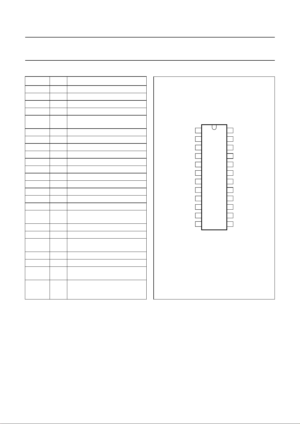
6 PINNING
SYMBOL PIN DESCRIPTION
FBL 1 fast blanking input for OSD insertion
OSD
1
OSD
2
OSD
3
CLI 5 input clamping and vertical blanking
V
I1
V
P
V
I2
GND 9 ground
V
I3
HFB 11 output clamping and blanking input
SDA 12 I
SCL 13 I
GNDX 14 ground signal, channels 1, 2 and 3
V
P3
V
O3
FB/R
3
V
P2
V
O2
FB/R
2
V
P1
V
O1
FB/R
1
LIM 24 subcontrast adjustment, contrast
2 OSD input, channel 1
3 OSD input, channel 2
4 OSD input, channel 3
input
6 signal input, channel 1
7 supply voltage
8 signal input, channel 2
10 signal input, channel3
2
C-bus serial data input/output
2
C-bus clock input
15 supply voltage, channel 3
16 signal output, channel 3
17 feedback input/reference voltage
output channel 3
18 supply voltage, channel 2
19 signal output, channel 2
20 feedback input/reference voltage
output, channel 2
21 supply voltage, channel 1
22 signal output, channel 1
23 feedback input/reference voltage
output, channel 1
modulation and beam current
limiting input
handbook, halfpage
FBL
1
OSD
2
1
OSD
3
2
OSD
4
3
CLI
5
V
6
I1
TDA4887PS
V
7
P
V
8
I2
GND
9
V
10
I3
HFB
11
SDA
12
MHB919
Fig.2 Pin configuration.
TDA4887PS
LIM
24
FB/R
23
1
V
22
O1
V
21
P1
FB/R
20
2
V
19
O2
V
18
P2
FB/R
17
3
V
16
O3
V
15
P3
GNDX
14
SCL
13
2001 Oct 19 7
Page 8

Philips Semiconductors Product specification
160 MHz bus-controlled monitor video
preamplifier
7 FUNCTIONAL DESCRIPTION
Referalsotoblockdiagram(Fig.1)anddefinitionsoflevels
and signals (Chapter 10).
7.1 Signal input stage
The RGB input signals are capacitively coupled into the
TDA4887PS from a low-ohmic source (75 Ω
recommended) and actively clamped to the internal
reference black level during signal black level. The signal
amplitude is 0.7V
high-ohmicinputimpedanceoftheTDA4887PSallowsthe
coupling capacitor to be relatively small (10 nF
recommended).Thecouplingcapacitoralsofunctionsasa
storage capacitor between clamping pulses. Very small
input currents will discharge the coupling capacitor
resulting in black output signals for missing input clamping
pulses.
Composite signals will not disturb normal operation
because a clipping circuit cuts all signal parts below black
level.
and should not exceed 1 V. The
i(b-w)
TDA4887PS
ThebrightnesssettingisalsovalidforOSDsignals.During
blanking and output clamping the video black level will be
blanked to the reference black level (brightness blanking).
The brightness information is inserted before the gain
potentiometers, background colour temperature will not
change with brightness setting (grey scale tracking).
7.2.2.2 Brightness control without grey scale tracking
Brightness control without grey scale tracking is selected
when control bit BRI = 1.
The brightness information will be mixed with the DAC
outputs for external black level restoration (FPOL = 1,
AC-coupled cathodes) or internal feedback reference
voltages (FPOL = 0, DC-coupled cathodes). This allows a
simplebus-controlledbrightnesssettingwithoutgreyscale
tracking. With AC-coupled cathodes this is equivalent to
brightness control via grid G1.
7.2.3 GAIN CONTROL AND GREY SCALE TRACKING
The gain control is driven by an 8-bit DAC via the I2C-bus.
A fast signal blanking circuit included in the input stage is
driven by several blanking pulses (see Section 7.6) and
control bit DISV = 1. During the off condition the internal
reference black level is inserted instead of the input
signals.
7.2 Electronic potentiometer stages
7.2.1 CONTRAST CONTROL
The contrast control is driven by an 8-bit DAC via the
I2C-bus. The input signals related to the internal reference
black level can be adjusted simultaneously by contrast
control with a control range of 32 dB (typical). The nominal
setting is for maximum contrast.
7.2.2 BRIGHTNESS CONTROL
7.2.2.1 Brightness control with grey scale tracking
The brightness control is driven by an 8-bit DAC via the
I2C-bus; brightness control with grey scale tracking is
selected when control bit BRI = 0.
With brightness control, the video black level is shifted in
relation to the reference black level simultaneously for all
three channels. With a negative setting (up to 10% of the
maximum signal amplitude) dark signal parts will be lost in
ultrablack;forpositivesettings(upto33%of the maximum
signal amplitude) the background will alter from black to
grey. At nominal brightness setting (40H) there is no shift.
Gain control is used for white point adjustment (correction
for different voltage-to-light amplification of the three
colour channels) and therefore individually for R, G and B.
The video signals related to the reference black level can
be gain-controlled within a range of 14 dB (typical). This
range is large enough to accommodate the maximum
output amplitude for different applications. The nominal
setting is maximum gain. The gain setting is also valid for
OSD signals and brightness shift (BRI = 0), therefore the
complete ‘grey scale’ is effected by gain control.
7.3 Output stage
In the output stage the nominal input signal will be
amplifiedtoprovide a 4.6 V (typical) output colour signal at
maximumcontrastandmaximumgainsettings.Reference
or pedestal black levels are adjusted by output clamping.
In order to achieve fast rise and fall times of the output
signals with minimum crosstalk between the channels,
each signal stage has its own supply voltage pin.
2001 Oct 19 8
Page 9

Philips Semiconductors Product specification
160 MHz bus-controlled monitor video
preamplifier
7.4 Pedestal blanking
The pedestal blanking is driven by a 2-bit DAC via the
I2C-bus. Pedestal blanking inserts a negative output level
related to the reference black level (should always
correspond to the ‘extended cut-off voltage’ at the
cathode) during blanking and output clamping. In this way
retrace lines during vertical flyback are suppressed
(blanking to spot cut-off). The depth of pedestal blanking
(voltage difference between reference black level and
pedestal black level) is bus-controlled (2 bits, 0 to 13.5%
of the maximum colour signal) and does not change with
any other control or adjustment. The pedestal blanking
level is used for output clamping instead of the reference
black level (see Section 7.5). If the pedestal blanking level
is the most negative output signal and if the application is
for AC-coupled cathodes, a very simple black level
restoration with a DC diode clamp can be used.
7.5 Output clamping and feedback references
Theaimoftheoutputclampingistosetthereferenceblack
level of the signal outputs to a value which corresponds to
the ‘extended cut-off voltage’ of the CRT cathodes. With
missing output clamping pulses the integrated storage
capacitors will be discharged resulting in output signals
going to switch-off voltage. If using pedestal blanking, the
pedestal black level will be controlled by output clamping
(see Fig.5). It is therefore not allowed to change the
pedestal depth after black level adjustment of the monitor.
Feedback references are driven via the I2C-bus and
controlled by an 8-bit DAC for DC feedback references or
by a 3-bit DAC for AC feedback references:
1. DC-coupled cathodes (control bit FPOL = 0)
Thecathodevoltageisdividedbyavoltage divider and
fed back to the IC (pins FB/R1, FB/R2and FB/R3).
During the output clamping pulse it is compared with a
bus-controlled feedback reference voltage with a
range of approximately 5.75 to 3.95 V. Any difference
will lead to a reference black level correction
(subaddress 0BH = 00H) or pedestal black level
correction (subaddress 0BH ≠ 00H) by charging or
discharging the integrated capacitors that store the
black level information between the output clamping
pulses. The DC voltages of the output stages should
be designed in such a way that the reference black
level/pedestal black level is within the range of
0.5 to 2.4 V at the preamplifier output.
TDA4887PS
For correct operation it is necessary that there is
enough headroom for ultra black signals (negative
brightnesssettingandpedestalblanking). Any clipping
with the video supply voltage at the cathode can
disturb the signal rise/fall times or the black level
stabilization.
After power-on, the control bit FPOL is set to logic 1
and all alignment registers are set to logic 0 resulting
in the reference black level at its lowest level (0.53 V)
with no output signal. Normal operation starts after all
data registers have been refreshed via the I2C-bus.
Brightness control with grey scale tracking (control bit
BRI = 0) can be used as well as brightness control
without grey scale tracking (control bit BRI = 1) using
the mixing function of bus-controlled brightness offset
(0 to −1.4 V) to feedback reference voltages
(see Section 7.2).
2. AC-coupled cathodes (control bit FPOL = 1)
For applications with AC-coupled cathodes the signal
outputs are fed back internally. During the output
clamping pulse they are compared with a bus
controlled feedback reference voltage (0.5 to 1.9 V).
These values ensure a good adaptability to both
discrete and integrated post amplifiers.
For black level restoration, the DAC outputs (FB/R1,
FB/R2and FB/R3) with a range of approximately
3.95 to 5.75 V can be used. Pedestal blanking is
recommended because it allows use of a simple
restoration circuit. After power-on, the DAC outputs
will be at maximum output voltage (register value
logic 0),sowhenusinganon-invertingamplifierforthe
reference voltages the monitor will start with black.
Brightness control with grey scale tracking (control bit
BRI = 0) can be used as well as simple brightness
control without grey scale tracking (control bit BRI = 1)
using the mixing function of bus controlled brightness
offset (0 to −1.4 V) to DAC output voltages
(see Section 7.2).
2001 Oct 19 9
Page 10

Philips Semiconductors Product specification
160 MHz bus-controlled monitor video
preamplifier
7.6 Clamping and blanking pulses
There are two pins for clamping and blanking purposes
(pins CLI and HFB):
1. Pin CLI (input clamping, vertical blanking)
The pin CLI of TDA4887PS can be connected directly
to pin CLBL of e.g. TDA4855 sync processor for input
clamping pulses and vertical blanking pulses.
Input clamping pulses and blanking pulses are
completely separated from the sandcastle input, that
means there is normally (outside detected vertical
blanking) no blanking during input clamping and the
clamping pulse is not suppressed during vertical
blanking.
The input pulse is scanned with two thresholds:
a) 1.4 V (typical) for vertical blanking
b) 3 V (typical) for input clamping.
In order to separate the vertical blanking pulse from
the sandcastle pulse it is necessary that the input
clamping pulse has rise/fall times faster than 75 ns/V
during the transition from 1.2 to 3.5 V and vice versa.
Theleadingedgeoftheinternalverticalblankingpulse
is delayed by typically 270 ns (after the end of an input
clampingpulseorthebeginningofaseparateblanking
pulse), the trailing edge is delayed by typically 115 ns.
During the vertical blanking pulse signal blanking,
brightness blanking and pedestal blanking will be
activated. In buffered mode, the leading edge of the
internal vertical blanking pulse is used to synchronize
data transmitted via the I2C-bus (see Section 7.10.1).
For correct input clamping the input signals have to be
at black level during the input clamping pulse.
2. Pin HFB (output clamping and blanking)
The input pulse (e.g. horizontal flyback pulse) is
scanned with two thresholds. If the input pulse
exceeds the first threshold (typically 1.4 V) signal
blanking, brightness blanking and pedestal blanking
will be activated. If the input pulse exceeds the second
threshold (typically 3 V) output clamping will be
activated additionally.
Especially for applications with DC-coupled cathodes
(FPOL = 0), it is useful that the leading edge of the
(internal) clamping pulse is slightly delayed with
respect to the leading edge of the (internal) blanking
pulse in order to avoid initial misclamping due to the
delay of the feedback signal from the cathodes.
TDA4887PS
7.7 On Screen Display insertion and OSD contrast
On Screen Display (OSD) insertion and OSD contrast are
controlled by a 4-bit DAC driven via the I2C-bus.
If the fast blanking input signal at pin FBL exceeds the
threshold (typically 1.4 V) the input signals are blanked
(signal blanking) and OSD signals are enabled. Then, any
signal at pins OSD1, OSD2 or OSD3 exceeding the same
threshold will create an insertion signal with an amplitude
of 100% of the maximum colour signal. The amplitude can
becontrolled by OSD contrast (driven via the I2C-bus)with
a range of 12 dB. The OSD signals are inserted at the
samepoint as the contrast-controlled input signals andwill
be treated with brightness and gain control as with normal
input signals.
Identical pulses at OSD signal input pins and FBL have to
be handled very carefully. Each difference in pulse delay
at the inputs will produce glitches at pulse edges at signal
outputs.
When control bit DISO = 1 the OSD signal insertion and
fast blanking (pin FBL) are disabled.
7.8 Subcontrast adjustment, contrast modulation
and beam current limiting
The pin LIM is a linear contrast control pin which allows
subcontrastsetting,contrastmodulationandbeamcurrent
limiting. The maximum contrast is defined by the actual
I2C-bus setting. Input signals at pin LIM act on video and
OSD signals and do not affect the contrast bit resolution.
If the pin is not used it should be decoupled with a
capacitor or tied to the supply voltage.
7.8.1 BEAM CURRENT LIMITING
The open-circuit voltage is approximately 5 V, contrast
reduction starts at input voltages <4.4 V (typical) and
signal amplification will be reduced with descending input
voltages. The input resistance of pin LIM is very high to
makeitpossibletochooseatimeconstant sufficient for the
open-circuit voltage to recover through the application.
7.8.2 SUBCONTRAST
In order to fit the maximum signal amplification to the post
amplifier gain, an input voltage of <4.4 V can be used.
7.8.3 CONTRAST MODULATION
To achieve brightness uniformity over the screen, scan
dependent contrast modulation is possible. The nominal
input voltage should be <4.4 V having enough margin for
positive and negative modulation.
2001 Oct 19 10
Page 11

Philips Semiconductors Product specification
160 MHz bus-controlled monitor video
preamplifier
7.9 I2C-bus control
The TDA4887PS contains an I2C-bus receiver for several
control functions:
• Contrast register with control bits BRI, FPOL, DISV and
DISO
• Brightness control with 8-bit DAC
• Contrast control with 8-bit DAC
• OSD contrast control with 4-bit DAC
• Gain control for each channel with 8-bit DAC
• Internal feedback reference and external reference
voltage control for each channel with 8-bit DAC
• Black level for AC coupling with 3-bit DAC
• Depth of pedestal blanking with 2-bit DAC.
After power-up and after internal power-on reset of the
I2C-bus, the registers are set to the following values (for
most applications these settings guarantee a blackscreen
after power-up):
• Control bit FPOL set to logic 1
• Control bits BRI, DISVand DISO set to logic 0
• All other alignment registers set to logic 0 (minimum
value for control registers).
After an intermediate power dip, all registers are set to
theirinitial values and an internal Power-on reset bit will be
set with the consequence that the device will give no
acknowledge on the data byte after being first addressed.
The Power-on reset bit will be reset if the control register
is addressed. It is recommended to then refresh all
registers by using the auto-increment function.
TDA4887PS
7.10 I2C-bus data buffer
7.10.1 BUFFERED MODE
Adjustmentsvia the I2C-busare synchronized with vertical
blanking pulse at CLI:
• Most significant bit (MSB) of subaddress is set to logic 1
• Only one I2C-bus transmission in buffered mode is
accepted before the start of the vertical blanking pulse;
following transmissions receive no acknowledge
• Received data is stored in one internal 8-bit buffer
• Adjustments will take effect with detection of the first
vertical blanking pulse after the end of the
acknowledged I2C-bus transmission
• Waiting for vertical blanking pulse in buffered mode can
be interrupted by Power-on reset
• Auto-increment is not possible
• Buffered mode should be used for user adjustments
such as contrast, OSD contrast and brightness when a
picture is visible on the monitor.
7.10.2 DIRECT MODE
Adjustments via the I2C-bus take effect immediately:
• Most significant bit (MSB) of subaddress is set to logic 0
• Number of I2C-bus transmissions in direct mode is
unlimited
• Adjustments take effect directly at the end of each
I2C-bus transmission
• Direct mode can be used for all adjustments but large
changes of control values may appear as visual
disturbances in the picture on the monitor
• Auto-increment is possible
• Vertical blanking pulse is not necessary.
2001 Oct 19 11
Page 12

Philips Semiconductors Product specification
160 MHz bus-controlled monitor video
TDA4887PS
preamplifier
8 LIMITING VALUES
In accordance with the Absolute Maximum Rating System (IEC 60134).
SYMBOL PARAMETER CONDITIONS MIN. MAX. UNIT
V
P
V
P(n)
V
i(n)
V
ext
I
o(n)(av)
I
o(n)(M)
P
tot
T
stg
T
amb
T
j
V
ESD
supply voltage (pin 7) 0 8.8 V
supply voltage; channels 1, 2 and 3
0 8.8 V
(pins 21, 18 and 15)
input voltage; channels 1, 2 and 3
−0.1 V
P
V
(pins 6, 8 and 10)
external DC voltage applied to
pins 1 to 4 −0.1 V
pins 5 and 11 −0.1 V
pins 12 and 13 −0.1 V
pins 23, 20 and 17 −0.1 V
P
+ 0.7 V
P
P
+ 0.7 V
P
V
V
pins 22, 19 and 16 note 1 note 1
pin 24 −0.1 V
averageoutput current; channels 1, 2 and 3
− 20 mA
P
V
(pins 22, 19 and 16)
peak output current channels 1, 2 and 3
− 50 mA
(pins 22, 19 and 16)
total power dissipation − 1400 mW
storage temperature −25 +150 °C
ambient temperature −20 +70 °C
junction temperature −25 +150 °C
electrostatic handling voltage for all pins
machine model note 2 −250 +250 V
human body model note 3 −3000 +3000 V
Notes
1. No external voltages.
2. Equivalent to discharging a 200 pF capacitor via a 0.75 µH inductance (
3. Equivalent to discharging a 100 pF capacitor via a 1500 Ω series resistor (
“SNW-FQ-302B”
“SNW-FQ-302A”
).
).
9 THERMAL CHARACTERISTICS
SYMBOL PARAMETER CONDITIONS VALUE UNIT
R
R
th(j-a)
th(j-c)
thermal resistance from junction to ambient in free air 55 K/W
thermal resistance from junction to case 5 K/W
2001 Oct 19 12
Page 13

Philips Semiconductors Product specification
160 MHz bus-controlled monitor video
TDA4887PS
preamplifier
10 CHARACTERISTICS
All voltages and currents are measured in a dedicated test circuit (see Fig.17) optimized for best high frequency
performance; all voltages are measured with respect to GND (pins 9 and 14); VP=V
T
=25°C; nominal input signals [0.7 V (p-p) at pins 6, 8 and 10]; maximum colour signals at signal outputs (pins 22,
amb
19 and 16); reference black level (V
) approximately 0.7 V; nominal setting for brightness; maximum settings for
bl(ref)
OSD contrast, contrast and gain; no subcontrast, modulation of contrast or limiting (V
(pin 1 connected to ground); notes 1 to 3; unless otherwise specified.
SYMBOL PARAMETER CONDITIONS MIN. TYP. MAX. UNIT
Supplies
V
V
P
P(SO)
supply voltage (pin 7) 7.6 8.0 8.8 V
supply voltage threshold at
note 1 6.8 7.0 7.2 V
pin 7 at which signal outputs
are switched off
I
P
V
P(n)
supply current (pin 7) note 4 − 25 30 mA
supply voltage; channels 1,
7.6 8.0 8.8 V
2 and 3 (pins 21, 18 and 15)
I
P(n)
supply current; channels 1,
2 and 3 (pins 21, 18 and 15)
pins 22, 19 and 16
open-circuit;
V
bl(n)(ref)
= 0.7 V;
− 20 25 mA
notes 4 and 5
2
Input clamping and vertical blanking input, validation of buffered I
V
CLI
input clamping and vertical
blanking input signal
notes 6 and 7
no vertical blanking,
C-bus data (CLI; pin 5)
−0.1 − +1.2 V
no input clamping
vertical blanking,
1.6 − 2.6 V
no input clamping
input clamping,
3.5 − V
no vertical blanking
I
CLI
input current V
=1V −−0.2 −µA
CLI
pin 5 connected to ground;
−80 −45 −30 µA
note 8
= −0.1 V; note 8 −250 −135 −100 µA
V
CLI
t
r/f5
rise/fall time for input
note 6; see Fig.7 −−75 ns/V
clamping pulse; disable for
vertical blanking
t
W(CLI)
width of input clamping
200 −− ns
pulse
t
W(I2C)(valid)
t
d(I2C)(valid)
width of vertical blanking
pulse for validation of
buffered I2C-bus data
delay between leading edge
of vertical blanking pulse
and validation of buffered
I2C-bus data
leading and trailing edge
threshold V
CLI
= 1.4 V;
note 7
I2C-bus buffered mode
transmission completed;
leading edge threshold
V
= 1.4 V; note 7;
CLI
10 −− µs
−−2µs
see Fig.7
= 8 V (pins 7, 21, 18 and 15);
P1,2,3
≥ 5 V); no OSD fast blanking
LIM
P
V
2001 Oct 19 13
Page 14

Philips Semiconductors Product specification
160 MHz bus-controlled monitor video
TDA4887PS
preamplifier
SYMBOL PARAMETER CONDITIONS MIN. TYP. MAX. UNIT
t
dead(I2C)
t
dl5
t
dt5
Output clamping and blanking input (HFB; pin 11)
V
HFB
I
HFB
t
W(HFB)
Video signal inputs; channels 1, 2 and 3 (pins 6, 8 and 10)
V
i(n)(b-w)
I
i(n)
Signal blanking
α
ct(blank)
I2C-bus receiver dead time
after synchronizing vertical
blanking pulse following a
completed I2C-bus buffered
mode transmission
delay between leading
edges of vertical blanking
input pulse and signal
blanking at signal outputs
delaybetween trailing edges
of vertical blanking input
pulse and signal blanking at
signal outputs
output clamping and
blanking input signal
input current V
width of output clamping
pulse
input voltage; black-to-white
value (pins 6, 8 and 10)
DC input current
(pins 6, 8 and 10)
crosstalk suppression from
input to output during
blanking
leading edge threshold
V
= 1.4 V; note 7
CLI
V
< 0.8 V; input pulse
HFB
15 −− µs
− 270 − ns
rising and falling edges
= 50 ns/V; threshold for
vertical blanking with rising
edge V
= 1.4 V; threshold
CLI
for vertical blanking with
falling edge V
CLI
=3V;
see Fig.7
V
< 0.8 V; input pulse
HFB
− 115 − ns
falling edge = 50 ns/V;
threshold V
CLI
= 1.4 V;
see Fig.7
note 9
no blanking, no output
−0.1 − +0.8 V
clamping
blanking, no output
2 − 2.6 V
clamping
blanking, output clamping 3.5 − V
= 0.8 V −−0.4 −µA
HFB
pin 11 connected to ground;
−80 −45 −30 µA
P
note 8
V
= −0.1 V; note 8 −250 −135 −100 µA
HFB
V
=3V 1 −− µs
HFB
− 0.7 1.0 V
no input clamping;
V
i(n)=Vi(n)(clamp)
T
= −20 to +70 °C
amb
;
during input clamping;
V
i(n)=Vi(n)(clamp)
±0.7 V
control bit DISV = 1;
0.02 0.20 0.35 µA
±350 ±420 ±500 µA
20 −− dB
f = 80 MHz
control bit DISV = 1;
10 −− dB
f = 120 MHz
V
2001 Oct 19 14
Page 15

Philips Semiconductors Product specification
160 MHz bus-controlled monitor video
TDA4887PS
preamplifier
SYMBOL PARAMETER CONDITIONS MIN. TYP. MAX. UNIT
Clipping of negative input signals (measured at signal outputs)
∆V
clipp
offset during sync clipping
related to maximum colour
signal
Contrast control; see Fig.8 and note 11
δ
C
colour signal related to
maximum colour signal
∆G
track
tracking of output colour
signals of channels 1,
2 and 3
Fast blanking (pin 1) and OSD signal insertion; channels 1, 2 and 3 (pins 2, 3 and 4); note 13
V
FBL
fast blanking input signal
(pin 1)
V
OSDn
OSD input signal
(pins 2, 3 and 4)
t
r(OSDn)
rise time of OSD colour
signals (pins 22, 19 and 16)
t
f(OSDn)
fall time of OSD colour
signals (pins 22, 19 and 16)
t
g(n)(CO)
width of (negative going)
OSD signal insertion glitch,
leading edge
(pins 22, 19 and 16)
t
g(n)(OC)
width of (negative going)
OSD signal insertion glitch,
trailing edge (pins 22, 19
and 16)
δV
OSDn
overshoot/undershoot of
OSD colour signal related to
actual OSD output pulse
amplitude (pins 22, 19
and 16)
V
OSDn(max)
maximumOSD colour signal
related to maximum colour
signal (pins 22, 19 and 16)
V
i(n)=Vi(n)(clamp)
;
− 0.6 1.2 %
sync amplitude = 0.3 V;
note 10; see Fig.3
FFH (maximum) − 0 − dB
00H (minimum) −−45 − dB
FFH to 40H; note 12 − 0 0.5 dB
no video signal blanking;
0 − 1.1 V
OSD signal insertion
disabled
video signal blanking;
1.7 − V
P
OSD signal insertion
enabled
V
> 1.7 V
FBL
no internal OSD signal
0 − 1.1 V
insertion
internal OSD signal
1.7 − V
P
insertion
10 to 90% amplitude; pulse
− 34 ns
leading edge = 1.2 ns/V
90 to 10% amplitude; pulse
− 47 ns
falling edge = 1.2 ns/V
identical pulses at fast
046ns
blanking input (pin 1) and
OSD signal inputs
(pins 2, 3 and 4)
identical pulses at fast
056ns
blanking input (pin 1) and
OSD signal inputs (pins 2, 3
and 4)
pulse with 1.2 ns/V at OSD
− 610 %
signal inputs (pins 2, 3
and 4)
maximum OSD contrast;
90 96 110 %
maximum gain
V
V
2001 Oct 19 15
Page 16

Philips Semiconductors Product specification
160 MHz bus-controlled monitor video
TDA4887PS
preamplifier
SYMBOL PARAMETER CONDITIONS MIN. TYP. MAX. UNIT
OSD contrast control; see Fig.9 and note 14
δ
OC
OSD colour signal related to
maximum OSD colour signal
Subcontrast adjustment, contrast modulation and beam current limiting (pin 24); see Fig.8 and note 15
V
LIM(nom)
V
LIM(start)
nominal input voltage pin 24 open-circuit 4.7 5.0 5.3 V
starting voltage for linear
contrast and OSD contrast
reduction
V
LIM(stop)
stop voltage for linear
contrast and OSD contrast
reduction
B
LIM
bandwidth of contrast
modulation
I
LIM(max)
maximum input current V
Brightness control; see Figs 10, 12 and 14 and notes 16 and 17
∆V
bl(n)
difference between video
black level and reference
black level at signal outputs
related to maximum colour
signal
∆V
DA(n)
DAC output voltage shift
(pins 23, 20 and 17)
Gain control; see Fig.11 and note 18
δ
G
video signal related to video
signal at maximum gain
Pedestal blanking; see Fig.5 and note 19
∆V
bl(n)(PED-VID)
difference between pedestal
black level and video black
level at nominal brightness,
measured at signal outputs
(pins 22, 19 and 16) related
to maximum colour signal
0FH (maximum) − 0 − dB
00H (minimum) −14 −12 −10 dB
4.2 4.4 4.8 V
−40 dB below maximum
1.5 2.0 2.5 V
colour signal (contrast
setting FFH)
−3dB 4 −− MHz
=0V −1 − +1 µA
LIM
FFH (maximum); BRI = 0 28 33 38 %
40H (nominal); BRI = 0 −2 0 +2 %
00H (minimum); BRI = 0 −12 −10 −8%
FPOL = 1, see DAC output
voltages for AC coupling or
feedback reference voltage
shift; FPOL = 0, see internal
feedback reference voltage
for DC coupling
FFH (maximum); BRI = 1 −−1.4 − V
00H (minimum); BRI = 1 − 0 − V
FFH (maximum) − 0 − dB
00H (minimum) −15 −13.5 −12.5 dB
03H (maximum) −12 −13.5 − %
02H −8 −9 − %
01H −4 −4.5 − %
00H (minimum) − 0 − %
2001 Oct 19 16
Page 17

Philips Semiconductors Product specification
160 MHz bus-controlled monitor video
TDA4887PS
preamplifier
SYMBOL PARAMETER CONDITIONS MIN. TYP. MAX. UNIT
Signal outputs; channels 1, 2 and 3 (pins 22; 19 and 16)
V
o(n)(min)
minimum output voltage
level (pins 22, 19 and 16)
V
o(n)(max)
maximum output voltage
level (pins 22, 19 and 16)
arbitrary input signals,
contrast, brightness and
gain adjustments; without
load
I
o(n)(source)(max)
maximum output source
current (pins 22, 19 and 16)
R
o(n)
output resistance
(pins 22, 19 and 16)
V
o(n)(b-w)(max)
maximum output voltage
swing (black-to-white value);
channels 1, 2 and 3
maximum contrast;
maximum gain;
V
= 0.7 V; RL=2kΩ
i(n)(b-w)
(pins 22, 19 and 16)
I
o(n)(source)(M)
I
o(n)(sink)(M)
peak output source current
(pins 22, 19 and 16)
peak output sink current
(pins 22, 19 and 16)
during fast positive signal
transients
during fast negative signal
transients
S/N signal-to-noise ratio note 20 48 −− dB
Frequency response at signal outputs; channels 1, 2 and 3 (pins 22, 19 and 16)
t
r(n)
rise time of fast transients
(pins 22, 19 and 16)
input rise time=1ns;
10 to 90% amplitude;
RL=10kΩ; notes 21,
22 and 23;
2.8 V (p-p) signal
amplitude; C
=5pF
L
4.5 V (p-p) signal
amplitude; C
=5pF
L
4.5 V (p-p) signal
t
f(n)
fall time of fast transients
(pins 22, 19 and 16)
amplitude; C
input fall time = 1 ns;
90 to 10% amplitude;
=11pF
L
RL=10kΩ; notes 21,
22 and 23;
2.8 V (p-p) signal
amplitude; C
=5pF
L
4.5 V (p-p) signal
amplitude; C
=5pF
L
4.5 V (p-p) signal
amplitude; C
=11pF
L
0.01 0.05 0.1 V
V
− 2 − V
P(n)
− 1V
P(n)
−15 −− mA
65 75 90 Ω
4.2 4.6 4.9 V
−40 −− mA
−−20 mA
− 2.7 3.8 ns
− 3.2 4.2 ns
− 3.8 4.5 ns
− 3.6 4.5 ns
− 3.6 4.5 ns
− 56 ns
2001 Oct 19 17
Page 18

Philips Semiconductors Product specification
160 MHz bus-controlled monitor video
TDA4887PS
preamplifier
SYMBOL PARAMETER CONDITIONS MIN. TYP. MAX. UNIT
δV
o(n)
Crosstalk at signal outputs; channels 1, 2 and 3 (pins 22, 19 and 16)
α
ct(tr)(n)
α
ct(f)
Internal feedback reference voltage for DC coupling; see Fig.12 and note 26
V
ref(DC)
Output clamping, feedback inputs for DC coupling; FB/R1, FB/R2 and FB/R3 (pins 23, 20 and 17)
overshoot of output signal
pulse related to actual
output pulse amplitude
(pins 22, 19 and 16)
undershoot of output signal
pulse related to actual
output pulse amplitude
(pins 22, 19 and 16)
transient crosstalk
suppression
(pins 22, 19 and 16)
crosstalk suppression by
frequency
internal reference voltage for
negative feedback polarity
(without brightness control)
internal reference voltage for
negative feedback polarity
(with brightness control, see
also brightness control
∆V
DA(n)
)
input rise time=1ns;
−−10 %
maximum colour signal
input fall time = 1 ns;
−−10 %
maximum colour signal
input rise/fall time = 1 ns;
10 −− dB
note 24
f = 50 MHz; note 25 25 −− dB
f = 100 MHz; note 25 10 −− dB
FFH; FPOL = 0; BRI = 0 3.7 3.95 4.1 V
00H; FPOL = 0; BRI = 0 5.6 5.75 5.9 V
FFH; FPOL = 0; BRI = 1;
2.3 2.55 2.7 V
maximum brightness
00H; FPOL = 0; BRI = 1;
5.6 5.75 5.9 V
minimum brightness
I
FB/Rn(max)
V
bl(n)(ref)(min)
V
bl(n)(ref)(max)
∆V
bl(CRT)
∆V
bl(n)(lf)
maximum input current
(pins 23, 20 and 17)
during output clamping;
V
HFB
> 3.5 V;V
FB/Rn
= 0.5 V;
−500 −200 −60 nA
FPOL = 0
minimum reference black
V
> 3.5 V; FPOL = 0 0.01 0.1 0.5 V
HFB
level/minimum pedestal
black level
(pins 22, 19 and 16)
maximum reference black
V
> 3.5 V; FPOL = 0 2.0 2.8 4.0 V
HFB
level/maximum pedestal
black level
(pins 22, 19 and 16)
black level variation at CRT FPOL = 0; note 27 −−200 mV
black level decrease
between clamping pulses
FPOL = 0; f
δ = 10%
= 60 kHz;
line
− 0.1 − %
related to maximum colour
signal (pins 22, 19 and 16)
2001 Oct 19 18
Page 19

Philips Semiconductors Product specification
160 MHz bus-controlled monitor video
TDA4887PS
preamplifier
SYMBOL PARAMETER CONDITIONS MIN. TYP. MAX. UNIT
Output clamping; internal feedback (of signal outputs) reference voltage for AC coupling;
see Fig.13 and note 28
V
bl(n)(ref)
reference black level
voltage/pedestal black level
voltage (pins 22, 19 and 16)
DAC output voltages for AC coupling; FB/R
V
FB/Rn
DAC output voltage (without
brightness control)
DAC output voltage (with
brightness control, see also
brightness control ∆V
R
FB/Rn
I
FB/Rn(sink)(max)
I
FB/Rn(source)(max)
2
C-bus inputs; SDA (pin 12), SCL (pin 13); note 30
I
f
SCL
V
IL
V
IH
I
IL
I
IH
V
OL
I
SDA(ack)
output resistance FPOL = 1 − 100 −Ω
maximum sink current FPOL = 1 −−400 µA
maximum source current FPOL = 1 −−200 −µA
SCL clock frequency −−100 kHz
LOW-level input voltage 0 − 1.5 V
HIGH-level input voltage 3 − 5V
LOW-level input current VIL=0V −10 −− µA
HIGH-level input current VIH=5V −10 −− µA
LOW-level output voltage during acknowledge 0 − 0.4 V
SDA output current (pin 12)
DA(n)
during acknowledge
t
o(f)
V
th(POR)(r)
V
th(POR)(f)
output fall time V
threshold for Power-on resetonrising supply voltage − 1.5 2.0 V
threshold for Power-on reset
off
V
> 3.5 V; FPOL = 1
HFB
00H (minimum) 0.47 0.53 0.59 V
0FH (maximum) 1.83 1.89 1.95 V
, FB/R2 and FB/R3 (pins 23, 20 and 17); see Fig.14 and note 29
1
FFH; FPOL = 1; BRI = 0 3.7 3.95 4.1 V
00H; FPOL = 1; BRI = 0 5.6 5.75 5.9 V
FFH; FPOL = 1; BRI = 1;
2.3 2.55 2.7 V
maximum brightness
)
00H; FPOL = 1; BRI = 1;
5.6 5.75 5.9 V
minimum brightness
VOL= 0.4 V 3 −− mA
V
= 0.6 V 6 −− mA
OL
= 3 to 1.5 V; bus
SDA
capacitance C
SDA
= 400 pF
−−250 ns
falling supply voltage − 3.5 − V
rising supply voltage −−7V
falling supply voltage − 1.5 − V
2001 Oct 19 19
Page 20

Philips Semiconductors Product specification
160 MHz bus-controlled monitor video
TDA4887PS
preamplifier
Notes to the characteristics
1. Definition of levels (see Figs 3 to 5)
Reference black level:this is the level to which the input level is clamped during the input clamping pulse
(V
> 3.5 V). It is used internally as a reference for the gain settings. It can be observed on the outputs:
CLI
a) When the input is at black and the brightness setting is nominal (subaddress 01H = 40H) or control bit BRI = 1
b) During output blanking and clamping (V
(subaddress 0BH = 00H).
Video black level:this is the black level of the actual video. At the input it is still equal to the reference black level.
At the output it may deviate from it according to the brightness setting. Contrast setting leaves the video black level
unaltered. Gain setting biases the video black level due to its influence on brightness. This is important for correct
grey scale tracking. It can be observed at the outputs when the input is at black outside output blanking and clamping
pulses (V
HFB
< 0.8 V).
Pedestal black level: this is anultra black level which deviates from the reference black level by a bus controlled
amount. It can be observed at the output during output blanking and clamping (V
0BH ≠ 00H).
Switch-off voltage: this is the lowest signal voltage at outputs. The signals will be switched off by discharging the
internalblack level storage capacitors if thesupply voltage is less than V
the input is at black, the brightness setting is nominal and VP< 6.8 V (subaddress 01H = 40H).
Blanking level: this level equals reference black (subaddress 0BH 1= 00H) or pedestal black. It can be observed at
the outputs during output blanking and clamping (V
2. Explanation to black level adjustment:
The three reference black levels are aligned correctly when they are made equal to the ‘extended cut-off levels’ of
the three cathodes. Full raster and spot cut-off can only beachieved by enabling the pedestalblanking or by applying
a negative pulse to the grid G1.
Negative feedback for DC-coupled cathodes (control bit FPOL = 0): the actual blanking level on the outputs
depends on the external feedback application for output clamping. The loop will function correctly only if it is within
the control range of V
bl(n)(ref)(min)
to V
bl(n)(ref)(max)
blanking in a given application will not affect the blanking level, but instead shifts the video (and needs re-alignment
of the three black levels).
Positive feedback for AC-coupled cathodes (control bit FPOL = 1): the feedback loop for output clamping is
closed internally. The actual blanking level is bus controlled between 0.53 and 1.89 V (subaddress 0AH). It should
be noted that changing pedestal blanking will not affect the blanking level, but instead shifts the video (and
re-alignment of the three black levels is needed).
3. Definition of output signals (see Fig.6):
Colour signal: all positive voltages are referenced to black level at signal outputs.
Maximum colour signal:colour signal with nominal input signal 0.7V
gain setting.
Video signal: all positive voltages referred to reference black level at signal outputs. The video signal is the
superimposing of the brightness information (∆Vbl) and the colour signal.
4. The total supply current I
P(tot)=IP+IP1+IP2+IP3
4.4 mA/V and varies in the temperature range from −20 to +70 °C by approximately ±5% (V
5. The channel supply current IP1,IP2,IP3depends on the signal output current IO1,IO2,IO3, the channel supply voltage
V
P1,VP2,VP3
I
P(n)IPxIO(n)
and the signal output voltage VO1,VO2,VO3. With IPx=I
4.4 mA/V V
8V–()× 1 mA/V V
P(n)
> 3.5 V) if the pedestal blanking depth is set to zero
HFB
> 3.5 V; subaddress
HFB
.It can be observed at theoutputs when
P(SO)
> 3.5 V).
HFB
at pins 22, 19 and 16. It should be noted that changing pedestal
, maximum contrast setting and maximum
i(b-w)
depends on the supply voltage with a factor of approximately
= 0.7 V).
O(n)
O(n)
at I
P(n)
0.7 V–()×–++≈
O(n)
= 0, V
= 8 V and V
P(n)
O(n)
= 0.7 V:
2001 Oct 19 20
Page 21

Philips Semiconductors Product specification
160 MHz bus-controlled monitor video
TDA4887PS
preamplifier
6. Pin 5should be used for input clamping and blanking during verticalretrace (signal blanking, brightness blanking and
pedestal blanking). With a fast clamping pulse (transition between V
75 ns/V) no blanking will occur during input clamping.
For 75 ns/V < t
≤ 280 ns/V the generation of the internal blanking pulse is uncertain. For t
r/f5
internal blanking pulse will be generated.
If pin 5 is open-circuit, it will activate permanent input clamping and undefined blanking.
7. Pin 5 can be used to synchronize all adjustments via the I2C-bus (one by one). With a completed I2C-bus
transmission in buffered mode, only the leading edge of a vertical blanking pulse activates an adjustment (see also
Section 7.10).
After the adjustment has been activated (validation of buffered I2C-bus data) the I2C-bus will be reset and further
transmissions in direct or buffered mode are enabled.
I2C-bus transmissions in direct mode need no synchronization pulses.
8. Input voltages less than −0.1 V can produce internal substrate currents which disturb the leakage currents at the
signal inputs. An internal protection circuit creates a current for pin voltages of approximately 0 V or with negative
voltage. Feeding clamping and blanking pulses via a resistor (several kΩ) protects the pin from negative voltages.
9. Pin 11shouldbeusedforoutput clamping and/or blanking. If pin 11 is open-circuit, it will activate permanent blanking
and output clamping.
10. Composite signals will not disturb normal operations because an internal clipping circuit cuts all signal parts below
input reference black level (see Fig.3).
2
11. Contrast control acts on internal colour signals under I
C-bus control; subaddress 02H (bit resolution 0.4% of
contrast range).
= 1.2 to 3.5 V and 3.5 to 1.2 V in less than
CLI
> 280 ns/V the
r/f5
A
∆G
12.
track
A
: colour signal output amplitude in channel n = 1, 2 or 3 at any contrast setting.
n
A
: colour signal output amplitude in channel n = 1, 2 or 3 at maximum contrast setting and same gain setting.
n0
20 maximum of
× dB=
log
A
1
-------- -
A
20
×
10
-------- A
log
2
13. When OSD fast blanking is active and OSD inputs OSD
A
A
1
-------- -
A
30
×
-------- A
10
3
, OSD2and OSD3are HIGH (V
1
A
2
log
×
-------- -
A
20
A
-------- A
30
3
> 1.7 V, V
FBL
OSD(n)
> 1.7 V)
the OSD colour signals will be inserted in front of the gain potentiometers. This ensures a correct grey scale of all
video signals. The amplitudes of the inserted OSD signals can be controlled simultaneously by OSD contrast via the
I2C-bus.
The inserted black level change (∆Vbl) due to brightness control is not affected by OSD fast blanking.
14. OSD contrast control acts on inserted OSD colour signals under I2C-bus control; subaddress 03H (bit resolution
6.7% of OSD contrast range).
15. This pin can be used for subcontrast adjustment, beam current limiting and contrast modulation. Both the video and
OSD contrast are reduced simultaneously (see Figs 8 and 9). Because of the high-ohmic input impedance the pin
should be tied to a voltage of more than 5 V or decoupled with a capacitor (several nF) if not used.
16. Brightness control adds an I2C-bus controlled DC offset to the internal colour signal; subaddress 01H (bit resolution
0.4% of brightness range). When control bit BRI = 1 the internal gain dependent brightness control is switched off
and the feedback reference voltages (control bit FPOL = 0) or DAC output voltages for DC restoration (control bit
FPOL = 1) at the cathodes are shifted with brightness control.
17. The voltage difference between video black level and reference black level is related to the colour signal (see note 3)
with nominal 0.7 V (p-p) input signal, at maximum contrast (subaddress 02H = FFH) and for any gain setting.
This voltage difference (in Volts) is proportional to the gain setting (grey scale tracking). Therefore ∆Vbl(in percent)
is constant for any gain setting.The given values of ∆Vblare valid only for video blacklevels higher than the minimum
output voltage level V
o(n)(min)
.
2001 Oct 19 21
Page 22

Philips Semiconductors Product specification
160 MHz bus-controlled monitor video
TDA4887PS
preamplifier
18. Gain control acts on video signals and inserted OSD video signals under I2C-bus control; subaddress 04H
(channel 1), 05H (channel 2) and 06H (channel 3; bit resolution 0.4% of gain range respectively).
19. Pedestal blanking produces an ultra black level during blanking and output clamping which is the most negative
signal at the signal output pins. The pedestal depth can be selected by bus control, subaddress 0BH. The reference
black level which should correspond to the ‘extended cut-off voltage’ at the cathodes is approximately ∆V
higher (see Fig.5). The use of pedestal blanking with AC-coupled cathodes (control bit FPOL = 1) allows a very
simple black level restoration with a DC diode clamp instead of a complicated pulse restoration circuit.
20. The signal-to-noise ratio is calculated using the formula (range 1 to 120 MHz):
S
20
--- N
peak-to-peak value of the maximum signal output voltage
-------------------------------------------------------------------------------------------------------------------------------------------------------RMS value of the noise output voltage
dBlog×=
21. The following formula can be used to approximately determine theoutputrise/falltime for any input rise/fall time other
than 1 ns:
2
t
r/f, measured
22. The relationship between pixel rate and signal bandwidth is f
2
t
r/f (22,19,16)
2
t
r/f, input
1 ns[]
–()+=
2
−3dB
= 0.75 × f
, which is a compromise between
pixel
excellentandacceptablevideoperformance.The calculation of the pixel-related rise and fall times can be done using
0.35
the formula . Although this formula is valid for low-pass filters of first order only it is used
==
t
----------- -
r/f
f
3dB–
in most cases for simplified estimations. The pixel rate isa good approximation for many filter types.
0.35
---------------------------- -
0.75 f
×
pixel
f
=
pixel
0.35
---------------------
×
0.75 t
r
23. Rise and fall times depend on signal amplitude, temperature, external load, black level and supply voltage. The rise
time is affected if the top level of the signal pulse approaches the maximum output voltage level (high black level,
large signal amplitude or low supply voltage). The fall time depends on the black level (increase with decreasing
black level) and on large capacitiveloads. Low-ohmic pull-down loads at the outputs helps towards smaller fall times.
Rise and fall times increase with increasing ambient (or crystal) temperature. At maximum operating temperature,
rise and fall times are approximately 0.4 ns longer than at T
amb
=25°C.
24. Transient crosstalk between any two output pins:
a) Input conditions: any channel (channel A) with nominal input signal and 1 ns rise time. The inputs of the other
two channels (channels B) are capacitively coupled to ground. Gain setting at maximum (FFH). Contrast setting
at maximum (FFH). No limiting/modulation of contrast (V
LIM
≥ 4.8 V)
b) Output conditions: black level set to approximately 0.7 V for each channel at signal outputs. Output signals are
VA and VB respectively
bl(n)(PED-VID)
V
c) Transient crosstalk suppression:
α
ct(tr)
20
------ V
A
dBlog×=
B
25. Crosstalk by frequency between any two output pins:
a) Input conditions: any channel (channel A) with 0.2 V (p-p) sinusoidal input signal, DC-coupled to approximately
4.3 V, no input clamping. The inputs of the other two channels (channels B) are capacitively coupled to ground.
Gain setting at maximum (FFH). Contrast setting at maximum (FFH). No limiting/modulation of contrast
(V
≥ 4.8 V)
LIM
b) Output conditions: control bit FPOL = 1, subaddress 0AH set to 01H, no pedestal blanking, nominal brightness
setting. Output signals are VA and VB respectively
V
c) Crosstalk suppression:
ct(f)
20
α
------ V
A
dBlog×=
B
2001 Oct 19 22
Page 23

Philips Semiconductors Product specification
160 MHz bus-controlled monitor video
TDA4887PS
preamplifier
26. Control bit FPOL = 0: the internal feedback referencevoltages for DC control act under I2C-buscontrol; subaddress
07H(channel 1),08H(channel 2)and 09H (channel 3); bit resolution 0.4% of voltage range. Rising values of the data
bytes, e.g. 00H to FFH, correspond to rising values of the resulting reference black levels at signal outputs
(pins 22, 19 and 16). The internal feedback reference voltages can be measured at feedback inputs
(pins 23, 20 and 17) during output clamping (V
operative at reference black levels between the specified values of V
Control bit BRI = 1: the internal feedback reference voltagescan be shifted under I2C-buscontrol which allows easy
brightness control without grey scale tracking (see Section 7.2.2.2); subaddress 01H (bit resolution 0.4% of voltage
shift range). The superimposition of internal feedback reference and brightness control leads to a voltage output
range of 5.8 to 2.5 V.
27. Slow variations of video supply voltage V
A change of V
28. To adapt to different types of post amplifier, the internal feedback reference voltage for AC coupling (control bit
FPOL = 1) acts under I2C-bus control; subaddress 0AH (bit resolution 14.29%). The internal feedback reference
voltage can be measured at signal outputs (pins 22, 19 and 16) during output clamping (V
black level or pedestal black level.
29. The DAC output voltages act under I2C-bus control for control bit FPOL = 1; subaddress 07H (FB/R1), 08H (FB/R2)
and 09H (FB/R3); bit resolution 0.4% of voltage range respectively. Using an inverting amplifier for DC restoration,
rising values of the data bytes, e.g. 00H to FFH, correspond to changing the light output from dark to bright.
With control bit BRI = 1 the DAC output voltages can be shifted under I2C-bus control which allows easy brightness
control without grey scale tracking (see Section 7.2.2.2); subaddress 01H (bit resolution0.4% of voltage shift range).
The superimposition of black level control and brightness control leads to a voltage output range of 5.8 to 2.5 V.
30. All adjustments via the I2C-bus can be synchronized with vertical blanking pulse at pin CLI. This is called I2C-bus
transmission in buffered mode. Conversely the adjustments via the I2C-bus will take effect immediately in
direct mode.
The timing of I2C-bus transmissions in buffered mode is related to the vertical blanking. See Section 7.6 and note 7
for specification of vertical blanking input (pin 5).
with 5 V leads to a specified change of the cathode voltage.
CRT
CRT
> 3.5 V) in closed feedback loop. The feedback loop remains
HFB
o(n)bl(ref)(min)
will be suppressed at the CRT cathode by the clamping feedback loop.
and V
o(n)bl(ref)(max)
HFB
.
> 3.5 V); reference
2001 Oct 19 23
Page 24

Philips Semiconductors Product specification
160 MHz bus-controlled monitor video
preamplifier
handbook, full pagewidth
input video signal
with sync pulses
at pins 6, 8 and 10
input clamping pulses
at pin 5
output clamping
and blanking
input pulses
at pin 11
TDA4887PS
input reference
black level
the sync pulses are
clipped to reference
black level internally
MHA344
The input video signals have to be at black level during input clamping.
Fig.3 Definition of input signals.
2001 Oct 19 24
Page 25

Philips Semiconductors Product specification
160 MHz bus-controlled monitor video
preamplifier
handbook, full pagewidth
output clamping and
blanking input pulses
at pin 11
signal outputs
at pins 22, 19 and 16
maximum gain setting,
maximum contrast setting,
maximum/nominal/minimum
brightness setting
switch-off voltage
ground
TDA4887PS
(1)
(2)
(3)
video black levels at
maximum brightness
nominal brightness
minimum brightness
reference black level
maximum gain setting,
maximum brightness setting,
maximum/minimum
contrast setting
switch-off voltage
maximum brightness setting,
maximum contrast setting,
maximum/minimum
gain setting
switch-off voltage
(1) Maximum.
(2) Nominal.
(3) Minimum.
ground
ground
(1)
(3)
(1)
(3)
video black level
(maximum brightness)
reference black level
video black levels
(maximum brightness)
reference black level
MHB920
Fig.4 Definition of levels and functions of brightness, contrast and gain with no pedestal blanking.
2001 Oct 19 25
Page 26

Philips Semiconductors Product specification
160 MHz bus-controlled monitor video
preamplifier
handbook, full pagewidth
output clamping and
blanking input pulses
at pin 11
signal outputs
at pins 22, 19 and 16
no pedestal blanking
maximum gain setting,
maximum contrast setting,
maximum/minimum
brightness setting
switch-off voltage
ground
TDA4887PS
(1)
video black levels at
(2)
maximum brightness
minimum brightness
reference black level
pedestal blanking
maximum gain setting,
maximum contrast setting,
maximum/minimum
brightness setting
(1) Maximum.
(2) Minimum.
switch-off voltage
ground
(1)
(2)
Fig.5 Output signals with and without pedestal blanking.
video black levels at
maximum brightness
minimum brightness
reference black level
pedestal black level
MHB921
2001 Oct 19 26
Page 27

Philips Semiconductors Product specification
160 MHz bus-controlled monitor video
preamplifier
handbook, full pagewidth
video black levels at
maximum brightness
minimum brightness
(1) Maximum brightness setting.
(2) Minimum brightness setting.
colour signals
(1)
(2)
TDA4887PS
video signals
reference black level
MHB922
Fig.6 Definition of output signals at pins 22, 19 and 16: maximum gain setting, maximum contrast setting and
no pedestal blanking.
handbook, full pagewidth
3 V
t
input pulses at pin 5
internal pulse for
input clamping
vertical blanking pulses
at signal outputs
(brightness blanking at
maximum brightness setting)
t
dl5
t
dl5
r/f5
t
dl5
MHB944
≤ 75 ns/V
1.4 V
video
black level
reference
black level
Fig.7 Timing of pulses at pin 5 and derived pulses at maximum brightness setting.
2001 Oct 19 27
Page 28

Philips Semiconductors Product specification
160 MHz bus-controlled monitor video
preamplifier
handbook, full pagewidth
colour signal
amplitude
with respect to
maximum colour
signal amplitude
(dB)
0
−
3
−
6
−
12
−
45
00H
20H
40H 60H
80H A0H
(1)
contrast
modulation
range
(2)
(3)
C0H
contrast control data byte
E0H FFH
TDA4887PS
MHB945
(1) No contrast reduction.
(2) Partial contrast reduction by subcontrast, limiting or contrast modulation.
(3) Full contrast reduction by subcontrast, limiting or contrast modulation.
Fig.8 Contrast control characteristic with subcontrast, limiting or contrast modulation.
handbook, full pagewidth
OSD signal
amplitude
with respect to
maximum colour
signal amplitude
(%)
maximum OSD signal amplitude
96
maximum colour signal amplitude
24
00H 0FH
MHB946
(1)
(2)
(3)
OSD contrast control data byte
(1) No OSD contrast reduction.
(2) Partial OSD contrast reduction by subcontrast, limiting or contrast modulation.
(3) Full OSD contrast reduction by subcontrast, limiting or contrast modulation.
Fig.9 OSD contrast control characteristic with subcontrast, limiting or contrast modulation.
2001 Oct 19 28
Page 29

Philips Semiconductors Product specification
160 MHz bus-controlled monitor video
preamplifier
handbook, full pagewidth
difference of
video black level
and reference
black level
with respect to
maximum colour
signal amplitude
(%)
−10
33
0
00H
20H
(1)
40H 60H
(2)
80H A0H
MHB947
C0H
brightness control data byte
E0H FFH
TDA4887PS
(1) Nominal adjustment.
(2) Nominal brightness reference black level.
Fig.10 Brightness control characteristic; control bit BRI = 0.
handbook, full pagewidth
video signal gain
with respect to
maximum video
signal gain
100
(%)
20
00H
20H
40H 60H
80H A0H
C0H
gain control data byte
E0H FFH
MHB948
Fig.11 Gain control characteristic.
2001 Oct 19 29
Page 30

Philips Semiconductors Product specification
160 MHz bus-controlled monitor video
preamplifier
handbook, full pagewidth
5.75
internal feedback
reference voltage
(V)
4.35
3.95
2.55
0
00H
20H
40H 60H
(1)
(2)
80H A0H
brightness control;
8-bit DAC subaddress 01H
C0H
negative feedback reference data byte
E0H FFH
TDA4887PS
MHB949
(1) Control bit BRI = 0 or control bit BRI = 1 and minimum brightness setting (subaddress 01H at 00H).
(2) Control bit BRI = 1 and maximum brightness setting (subaddress 01H at FFH).
Fig.12 Internal feedback reference voltages for negative feedback (FPOL = 0).
handbook, full pagewidth
internal feedback
reference voltage
(V)
1.89
1.70
1.50
1.31
1.11
0.92
0.72
0.53
0
01H 02H 04H 05H 06H 07H03H
positive feedback reference data byte
MHB950
Fig.13 Internal feedback reference voltages for positive feedback (FPOL = 1).
2001 Oct 19 30
Page 31

Philips Semiconductors Product specification
160 MHz bus-controlled monitor video
preamplifier
handbook, full pagewidth
5.75
DAC output voltage
pins 23, 20, 17
(V)
4.35
3.95
2.55
0
00H
20H
40H 60H
feedback reference data byte; subaddresses 07H, 08H and 09H
(1)
(2)
80H A0H
brightness control;
8-bit DAC subaddress 01H
C0H
TDA4887PS
MHB951
E0H FFH
(1) Control bit BRI = 0 or control bit BRI = 1 and minimum brightness setting (subaddress 01H at 00H).
(2) Control bit BRI = 1 and maximum brightness setting (subaddress 01H at FFH).
Fig.14 DAC output voltages (control bit FPOL = 1).
2001 Oct 19 31
Page 32

Philips Semiconductors Product specification
160 MHz bus-controlled monitor video
TDA4887PS
preamplifier
11 I2C-BUS PROTOCOL Table 1 Slave address
(1)
A6
10001000
Notes
1. Address bit.
2. Write bit.
Table 2 Slave receiver format
(1)
S
Notes
1. START condition.
2. A = acknowledge.
After an intermediate power dip all registers are set to their initial values (see note 3 at Table 4) and an internal
power-on reset bit will be set with the consequence that the device will give no acknowledge on the data byte after
a first addressing. The power-on reset bit will be reset if the control register is addressed. It is recommended to then
refresh all registers by using the auto-increment function.
3. All subaddresses within the range 00H to 0BH are automatically incremented. The subaddress counter wraps
around from 0BH to 00H. For subaddresses within the range 80H to 8FH no auto-increment takes place.
Subaddresses outside the ranges 00H to 0BH and 80H to 8BH are acknowledged by the device but no
auto-increment or any other internal operation takes place.
4. Single data byte in case of no auto-increment of subaddresses. More than one data byte with auto-increment of
subaddresses.
5. STOP condition.
(1)
A5
A4
SLAVE ADDRESS A
(1)
(2)
(1)
A3
SUBADDRESS
(1)
A2
(3)
A DATA BYTE
A1
(1)
(1)
A0
(4)
AP
W
(2)
(5)
2001 Oct 19 32
Page 33

Philips Semiconductors Product specification
160 MHz bus-controlled monitor video
preamplifier
Table 3 Subaddress byte format
SUBADDRESS
FUNCTION
DIRECT
MODE
Control register 00H 80H B
Brightness control 01H 81H B
Contrast control 02H 82H B
OSD contrast control 03H 83H B
Gain control channel 1 04H 84H B
Gain control channel 2 05H 85H B
Gain control channel 3 06H 86H B
Black level reference channel 1 07H 87H B
Black level reference channel 2 08H 88H B
Black level reference channel 3 09H 89H B
Black level for AC coupling 0AH 8AH B
Depth of pedestal blanking 0BH 8BH B
0CH to 0FH 8CH to 8FH not used
(1)
BUFFERED
MODE
TDA4887PS
SUBADDRESS BYTE
(2)S6(2)S5(2)S4(2)S3(2)S2(2)S1(2)S0(2)
S7
(3)
0000000
(3)
0000001
(3)
0000010
(3)
0000011
(3)
0000100
(3)
0000101
(3)
0000110
(3)
0000111
(3)
0001000
(3)
0001001
(3)
0001010
(3)
0001011
Notes
1. The most significant bit (MSB) of the subaddress enables an I
2
C-bus transmission in direct or in buffered mode
(see note 3). Subaddresses outside the ranges 00H to 0FH and 80H to 8FH are not used.
2. Subaddress bit.
3. Most significant bit of subaddress byte. I2C-bus transmission in direct mode: B = 0. I2C-bus transmission in
buffered mode: B = 1.
2001 Oct 19 33
Page 34

Philips Semiconductors Product specification
160 MHz bus-controlled monitor video
TDA4887PS
preamplifier
Table 4 Subaddress and data byte format
MODE
(1)
D7
(4)
(5)
(4)
D6
BRI X
D5
(4)
(5)
DATA BYTE
(4)
D4
(5)
X
SUBADDRESS
FUNCTION
BUFFERED
MODE
Control register 00H 80H X
Brightness control 01H 81H A17 A16 A15 A14 A13 A12 A11 A10 40H
Contrast control 02H 82H A27 A26 A25 A24 A23 A22 A21 A20 FFH
OSD contrast
03H 83H X
(5)X(5)
(5)
X
(5)
X
control
Gain control
04H 84H A47 A46 A45 A44 A43 A42 A41 A40 FFH
channel 1
Gain control
05H 85H A57 A56 A55 A54 A53 A52 A51 A50 FFH
channel 2
Gain control
06H 86H A67 A66 A65 A64 A63 A62 A61 A60 FFH
channel 3
Black level
07H 87H A77 A76 A75 A74 A73 A72 A71 A70 −
reference channel 1
Black level
08H 88H A87 A86 A85 A84 A83 A82 A81 A80 −
reference channel 2
Black level
09H 89H A97 A96 A95 A94 A93 A92 A91 A90 −
reference channel 3
Black level for
0AH 8AH X
(5)X(5)
(5)
X
(5)
X
AC coupling
Depth of pedestal
0BH 8BH X
(5)X(5)
(5)
X
(5)
X
blanking
(2)
NOMINAL
(5)
(4)
VALUE
08H
D3
(4)
D2
(4)
D1
(4)
D0
FPOL DISV DISO X
A33 A32 A31 A30 0FH
(5)
X
AA2 AA1 AA0 −
(5)
X
(5)
X
AB1 AB0 00
(3)DIRECT
Notes
1. See Table 3 (Subaddress byte format).
2. The least significant bit (LSB) of an analog alignment register is defined as AX0 (data bit D0).
3. Under certain conditions the nominal values lead to nominal colour signals, etc. (see notes 1 and 3 of
Chapter “Characteristics” and Figs 4 to 6).
After power-up and after internal Power-on reset of the I2C-bus the registers are set to the following values:
a) Control bit FPOL to logic 1.
b) Control bits DISV, DISO and BRI to logic 0.
c) All other alignment registers to logic 0 (minimum value for control registers).
4. Data bit.
5. X means don’t care but the bits are preferably set to logic 0 for software compatibility with other video ICs that have
the same slave address.
2001 Oct 19 34
Page 35

Philips Semiconductors Product specification
160 MHz bus-controlled monitor video
TDA4887PS
preamplifier
Table 5 Control register
BIT FUNCTION
DISO = 0 OSD signals enabled
DISO = 1 OSD signals disabled
DISV = 0 video signals enabled
DISV = 1 video signals disabled
FPOL = 0 negative feedback polarity; pins 23, 20 and 17 as feedback inputs; no external DAC voltage outputs
FPOL = 1 positive feedback polarity; pins 23, 20 and 17 as external DAC voltage outputs; internal feedback of
signal outputs
BRI = 0 internal brightness control with grey scale tracking
BRI = 1 Brightness control without grey scale tracking. With FPOL = 0 the brightness information is combined
with the internal feedback reference voltages. With FPOL = 1 the brightness information is combined
with the DAC output voltages for DC restoration at the cathodes.
2001 Oct 19 35
Page 36

Philips Semiconductors Product specification
160 MHz bus-controlled monitor video
preamplifier
handbook, full pagewidth
LOAD PRESET CONTROL BITS
LOAD FACTORY SETTINGS
BLACK LEVEL REFERENCES
OR EXTERNAL DAC VOLTAGES
LOAD USER PRESET VALUES
START
FPOL, BRI
DISV = 1
DISO = 1
GAIN
(CHANNEL 1, 2, 3)
(CHANNEL 1, 2, 3)
AC BLACK LEVEL
PEDESTAL DEPTH
CONTRAST
BRIGHTNESS
OSD CONTRAST
load from program
ROM code or EEPROM
load from EEPROM
load from EEPROM
TDA4887PS
(1) Only synchronized video should
be displayed. Each new mode
can be displayed by OSD.
(2) Data transmission should be
synchronized with vertical
blanking of the monitor.
DEFLECTION
CONTROL
IC LOCKED
yes
DISV = 0
DISO = 0
DISPLAY NEW MODE
DISO = 1
USER INPUT
yes
RESPONSE TO USER INPUTS
(CONTRAST, BRIGHTNESS, OSD CONTRAST)
DISO = 0
DISO = 1
DEFLECTION
CONTROL
IC LOCKED
yes
no
(1)
no
(2)
no
DISV = 1
MHB932
Fig.15 I2C-bus control flow chart.
2001 Oct 19 36
Page 37

Philips Semiconductors Product specification
160 MHz bus-controlled monitor video
preamplifier
12 TEST AND APPLICATION INFORMATION
handbook, full pagewidth
fast blanking
24
232
223
214
205
19
187
178
signal inputs
channel 1
channel 2
OSD
inputs
1
6
TDA4887PS
contrast modulation input
subcontrast setting
90 V
70 V
TDA4887PS
limiting input
Application with integrated
post amplifier, DC-coupled cathode
and negative feedback.
to cathode
BLACK LEVEL
RESTORATION
to cathode
Application with integrated
post amplifier, AC-coupled cathode
and black level restoration cicuit.
16
1510
14
13
output clamping
input clamping
vertical blanking
5 V
blanking
channel 3
9
11
12
8 V
pull-up
resistors
I2C-BUS
Fig.16 Basic applications for different kinds of post amplifiers with DC or AC coupling.
12.1 Test board
For high frequency measurements, a special test board
withonlya few external components can be built. It utilizes
the internal positive feedback of the output signals during
output clamping with control bit FPOL = 1. Figure 17
90 V
Application with discrete
post amplifier, DC-coupled
cathode and negative
feedback.
to cathode
MHB933
shows the test circuit and Figs 18 and 19 show the layout
and mounting of the double-sided printed-circuit board.
Most components are SMD-type. Short HF loops and
minimum crosstalk between channels and between signal
inputs and outputs are achieved by using properly shaped
ground areas.
2001 Oct 19 37
Page 38

Philips Semiconductors Product specification
160 MHz bus-controlled monitor video
preamplifier
5.6 Ω
100
1 kΩ
FBL
1
OSD
1
2
OSD
2
3
OSD
3
4
CLI
5
V
I1
6
TDA4887PS
V
P
7
100
pF
nF
V
GND
V
HFB
SDA
I2
8
9
I3
10
11
12
handbook, full pagewidth
FBL
OSD
1
OSD
2
OSD
3
CLI
V
I1
V
I2
V
I3
HFB
50
50
50
50
Ω
Ω
Ω
Ω
10 nF
150 pF
10 nF
150 pF
10 nF
150 pF
50 Ω
50 Ω
50 Ω
50 Ω
50 Ω
5 kΩ
J1
5 kΩ
J2
5 kΩ
J3
150pF10
0.47 µF
(63 V)
nF
TDA4887PS
LIM
24
10
kΩ
10
kΩ
10
kΩ
FB/R
1
solder pin
FB/R
2
solder pin
FB/R
3
solder pin
V
O1
V
O2
V
O3
FB/R
1
23
150
150
150
pF
pF
pF
channel 1
100
nF
channel 2
100
nF
channel 3
100
nF
1 kΩ
5.6 Ω
0.47 µF
(63 V)
5.6 Ω
0.47 µF
(63 V)
5.6 Ω
0.47 µF
(63 V)
3.3
3.3
pF
pF
3.3
pF
V
O1
22
V
P1
21
FB/R
2
20
V
O2
19
V
P2
18
FB/R
3
17
V
O3
16
V
P3
15
GNDX
14
SCL
13
SDA
5 V
SCL
10 nF
50
Ω
10 kΩ
10 kΩ
LIMAC
Fig.17 Test board utilizing internal positive feedback only (FPOL = 1).
2001 Oct 19 38
10 nF
10 kΩ
VPX
VP1 sense
VP sense
V
P
GND
VINDC
LIM
5 V
MHB934
Page 39

Philips Semiconductors Product specification
160 MHz bus-controlled monitor video
preamplifier
handbook, full pagewidth
TDA4887PS
103
81
150 pF
10 nF
10 kΩ
3.3 pF
5.6 Ω
1 kΩ
150 pF
10 kΩ
100
nF
10 kΩ
150 pF
10 kΩ
10 nF
V
O1
1 kΩ
−
0.47 µF
+
V
O2
V
O3
0.47 µF
0.47 µF
−
+
−
+
U19
5.6 Ω
5.6 Ω
5.6 Ω
MHB935
CLI
50 Ω
V
V
V
HFB
I1
I2
I3
OSD
3
50 Ω 50 Ω
50 Ω
10 nF
150 pF
10 nF
50 Ω
150 pF
5 kΩ
50 Ω
10 nF
5 kΩ
50 Ω
10 kΩ 10 kΩ
OSD
5 kΩ
J1
J2
+
0.47 µF
−
J3
2
150 pF
SCLSDA
OSD
1
50 Ω 50 Ω
TDA4887PS
50 Ω
FBL
3.3 pF
100 nF
3.3 pF
100 nF
LIMAC
Dimensions are in mm.
Fig.18 Printed-circuit top view shown with and without components mounted (for bottom view, see Fig.19).
2001 Oct 19 39
Page 40

Philips Semiconductors Product specification
160 MHz bus-controlled monitor video
preamplifier
handbook, full pagewidth
TDA4887PS
103
81
100 pF
100 nF
100 nF
100 pF
MHB217
Dimensions are in mm.
Fig.19 Printed-circuit bottom view shown with and without components mounted (for top view, see Fig.18).
2001 Oct 19 40
Page 41

Philips Semiconductors Product specification
160 MHz bus-controlled monitor video
preamplifier
12.2 Application board with monolithic
post amplifier
Figure 20showstheapplicationcircuitof TDA4887PS with
a modern monolithic video post amplifier and AC-coupled
CRT. The black level restoration circuit is designed for
TDA4887PS
80 V supply and use of I2C-bus controlled external
brightness setting. The 8 V supply voltage of the
preamplifier is made from 12 V on this board. Connectors
for video, sync, I2C-bus, OSD, clamping pulses, beam
current limiting and supply voltages are provided.
2001 Oct 19 41
Page 42

Philips Semiconductors Product specification
160 MHz bus-controlled monitor video
preamplifier
V
V2 80 V
V1 12 V
CLAMPING
BLANKING
Vff GND
GROUND
HOR SYNC
VERT SYNC
AQUADAG
CH 1
CH 2
OSD
CH 3
SDA
+
GND
SCL
VERT SYNC
HOR SYNC
CH 1
V
n.c.
n.c.
FBL
5 V
g2
1
2
3
4
5
R3
6
V
ff
7
8
g1
9
10
11
12
13
14
4
3
2
1
R9
100 Ω
4
3
2
5.1 V
1
R101
75 Ω
R5
1 kΩ
8 V
R6
1 kΩ
D1
R7
10 kΩR810 kΩ
C101
22 nF
100 nF
R103
33 Ω
5.6 Ω
330 nF
R302
1 kΩ
C1
R4
1 kΩ
R2
1 Ω
C2
R202
1 kΩ
handbook, full pagewidth
BEAM CUR LIM
2
I
C-BUS
7808
R102
1 kΩ
C3
100 nF
22 nF
100 Ω
100 Ω
R1
1 Ω
R15/H
2.7 kΩ
C7
R10
R11
R14
2.2 Ω
R16/H
2.7 kΩ
R12
100 Ω
1
2
3
4
5
6
TDA4887PS
7
8
9
10
11
12
C6
100 µF
C9
22 nF
24
23
22
21
20
19
18
17
16
15
14
13
L1 10 µH
L2 10 µH
8 V
C102
100 nF
C202
100 nF
C302
100 nF
R106
10 Ω
R206
10 Ω
R306
10 Ω
TDA4887PS
A
B
1.5 nFC12
C
D
E
F
G
H
I
R104
5.6 Ω
J
K
R204
5.6 Ω
L
M
R304
5.6 Ω
N
C201
VIDEO
INPUT
CH 2
CH 3
R201
75 Ω
R301
75 Ω
22 nF
C301
22 nF
R203
33 Ω
R303
33 Ω
MHB966
Fig.20 Application board with LM2435 (drawing is continued in Fig. 20).
2001 Oct 19 42
Page 43

Philips Semiconductors Product specification
160 MHz bus-controlled monitor video
preamplifier
handbook, full pagewidth
A
B
C
D
E
F
R13
G
4.7 Ω
C8
47 µF
H
I
J
K
L
M
N
C15
100 nF
C4
47 µF
C14
2 × 100 nF
C5
1 nF
(2 kV)
R305
10 Ω
4
5
6
7
8
9
C304
2.2 nF
LM2435
8 V
TR301
R205
10 Ω
C11
1 nF
(2 kV)
BC546
C204
2.2 nF
C10
1.5 nF
D109
BAV103
L108
R107
0.22 µH
22 Ω
1
R207
2
22 Ω
3
R307
22 Ω
R316
8 V
TR201
R313
270 Ω
TR302
R105
10 Ω
2.2 nF
68 kΩ
2 ×
BC546
8 V
C104
2 ×
L208
0.22 µH
L308
0.22 µH
R314
12 kΩ
TR202
R213
270 Ω
TR101
BAV103
BAV103
D303
BAW62
R315
150 kΩ
R216
68 kΩ
2 ×
BC546
D209
D309
R113
270 Ω
R214
12 kΩ
R318/H
68 Ω
D110
BAV103
D210
BAV103
D310
BAV103
C305
1 µF
(100 V)
BAW62
TR102
R317
10 kΩ
D203
R215
150 kΩ
R116
68 kΩ
R218/H
68 Ω
C106
1 µF
(63 V)
C206
1 µF
(63 V)
C306
1 µF
(63 V)
(100 V)
R114
12 kΩ
R217
10 kΩ
C205
1 µF
BAW62
R115
150 kΩ
D103
MHB967
R118/H
68 Ω
(100 V)
R119
1 MΩ
R219
1 MΩ
R319
1 MΩ
R117
10 kΩ
C105
1 µF
TDA4887PS
EHT
6
8
11
10
9571
V
foc
Fig.21 Application board with LM2435 (drawing continued from Fig. 20).
2001 Oct 19 43
Page 44

Philips Semiconductors Product specification
160 MHz bus-controlled monitor video
preamplifier
12.3 Building the application board
12.3.1 GENERAL
• Double-sided board
• Short HF loops by large ground plane on the rear
• SMD components with minimum parasitics.
12.3.2 VOLTAGE OUTPUTS
• Capacitive loads as small as possible
• Be aware of internal output resistance (typically 75 Ω).
12.3.3 SUPPLY VOLTAGES
• Capacitors as near as possible to the pins
• Use electrolytic capacitors with small serial resistance
and inductance.
12.3.4 FLASHOVER
High electric field strength is present between the gun
electrodes of picture tubes. In case of a flashover large
transient currents and voltages may damage electronic
components. It is therefore important to provide protective
circuits with spark gaps, series resistors and protection
diodes. Be aware that not only electronic components that
are directly connected to the tube socket are endangered
if interconnection lines on the application board are
unfavourably routed.
12.4 Application hints
12.4.1 ALIGNMENT RECOMMENDATIONS USING BRIGHTNESS
CONTROL WITH GREY SCALE TRACKING
12.4.1.1 Introduction (philosophy of TDA4887PS)
With the TDA4887PS the user may change contrast,
brightness and even colour temperature (R, G, B gains) or
any combination at will. The ‘x,y’ colour point will remain
stable for the full grey scale. This feature is achieved in the
following way:
A change of brightness will cause a change of black
level which is proportional to the actual gain setting
Conversely, a change of gain setting will cause a
changeof black level that is proportional tothe deviation
of brightness from its nominal setting.
To benefit fully from this colour tracking feature, the
reference black levels of the video amplifiers must match
exactly to the cut-off points of the cathodes.
Re-adjustments of black level settings by the end user
should be avoided, because this will upset the tracking
feature.
TDA4887PS
12.4.1.2 Difficulty during monitor production
The factory cut-off alignment is done at a quite high level
(e.g.2.4 cd/m2).As a consequence it is not certain thatthe
reference black level will match the cut-off exactly after a
first black level adjustment. If then the R, G, B gains are
adjusted for the (x, y) white point at e.g. 102.8 cd/m2, the
white balance at 2.4 cd/m2 will have changed. So two or
more alignment cycles may be needed to achieve good
results.
12.4.1.3 Considerations for a single-pass factory
alignment
Thenominal brightness setting is 40H. In this condition the
black level equals reference black level and must match to
the CRT cut-off.
For a better understanding, discrete values for luminance,
video and feedback gain have been taken (these values
shouldberegardedasexamples).Forspecialapplications
actual values have to be taken instead.
White point must be aligned at maximum luminance
(e.g. at 102.8 cd/m2) with maximum contrast and nominal
brightness. It is recommended to use only a small white
square for white point alignment, to prevent variations of
the voltage at grid G1 (Vg1) and grid G2 (Vg2) and to
prevent unwanted activation of the automatic beam limiter
(ABL).
For practical reasons, alignment of the R, G, B reference
black levels must be done with a small amount of drive for
obtaining a luminance level of approximately 2.4 cd/m2.
This drive can be simulated by setting the brightness to a
certain value. Assuming 102.8 cd/m2 luminance with full
white video (100% drive) and a cathode characteristic with
gamma = 2.25, the drive for black level adjustment can be
shown as:
2.4
---------------------------
102.8
which corresponds to a brightness setting of B8H.
After black level adjustment for L = 2.4 cd/m2, the cathode
voltages are fixed and the cut-off voltages are set with
equal gain condition in all channels. During white point
adjustment the gains will be changed. In the factory
procedure for single pass adjustment, the luminance level
for black level alignment (2.4 cd/m2) is kept constant while
adjusting the gain settings. To achieve this, the black level
references are compensated by software and an
alignment computer (this compensation is for factory
alignment only and is not needed for any user change of
R, G, B gain).
1/2.25
100 = 18.8% drive×
2001 Oct 19 44
Page 45

Philips Semiconductors Product specification
160 MHz bus-controlled monitor video
preamplifier
Calculation of compensation (see Fig.22):
1. Gain adjustment is in 255 steps from 20 to 100%
which equates to 4.6 V per step at maximum contrast.
One step = which is equal to
0.8 4.6 V×
---------------------------255
187 mV at the cathode with video gain = 13 for the
white area.
2. For 18.8% drive (used for black level adjustment) the
output changes only 2.7 mV (35 mV at the cathode)
per gain step.
handbook, full pagewidth
FIXED
0.7 V
(nom.)
MAXIMUM
GAIN
4.6/0.7 V
14.4 mV=
CONTRAST
−40 dB
(0.5/100%)
255 steps
BRIGHTNESS
−10/30%
of 4.6 V
255 steps
TDA4887PS
3. The black level adjustment range (at feedback inputs)
is 1.9 V in 255 steps, which is 7.45 mV per step
(∆ black level of 97 mV at the cathode with feedback
1
gain =
is one step black level for orapproximately
three steps of gain.
3 × GAIN
20/100%
255 steps
⁄13). It follows that the optimum compensation
97
2.8=
-----35
signal
4.6 V
(max.)
VIDEO GAIN
≈13
amplitude
60 V (max.)
CRT
3 × BLACK REFERENCES
range 1.9 V
PREAMPLIFIER
255 steps
Fig.22 Signal amplification and feedback references.
12.4.1.4 Example of automatic factory alignment
This procedure shows a realization of the alignment
description, it depends on disposable equipment.
Gamma = 2.25, maximum luminance = 102.8 cd/m2,
video gain = 13, feedback gain =1⁄13, white D; see Fig.23.
1. Initialization
a) Set grid 2 voltage to minimum
b) Set R, G, B gains to the centre values (80H,
subaddresses 04H, 05H, 06H)
c) Set R, G, B black referencestocentrevalues(80H,
subaddresses 07H, 08H, 09H)
d) Set contrast to maximum (FFH, subaddress 02H).
FEEDBACK GAIN
5.75
to 3.95 V
≈1/13
≈25 V cut-off
level variation
MHB953
2. Vg2 and black levels
a) Set brightness to 18.8% drive (B8H,
subaddress 01H, control bit BRI=0)
b) Apply black video
c) Increase Vg2 manually until one colour appears
d) Activate the alignment computer
e) The computer will continuously adjust the R, G, B
black levels to meet the following three conditions:
x = 0.131
y = 0.329
the centre of the min/max setting remains at 80H
(this will leave some margin for the compensation
steps that follow)
f) Fine tuning of Vg2 (or Vg1) until Y = 2.4 cd/m2 with
the computer still active.
2001 Oct 19 45
Page 46

Philips Semiconductors Product specification
160 MHz bus-controlled monitor video
preamplifier
3. R, G, B gains (white point)
a) Set brightness at nominal (40H)
b) Apply full video white area (700 mV)
c) Activate the computer
d) The computer will adjust the R, G, B gains to meet
the following three conditions:
x = 0.313
y = 0.329
Y = 102.8 cd/m
Foreach 3 (2.8) gain increments, the computerwill
decrement the black references by one step.
handbook, full pagewidth
cathode
voltage
(V)
2
80
70
black
60
18.8%
TDA4887PS
The effect on cathode voltages is demonstrated in Fig.23.
After step 2 the voltages at 18.8% drive are correct but not
those at 100% drive (white) and 0% (black). After step 3
the voltages at 18.8% drive have not changed but white as
well as black voltages are correct now. Any brightness
setting (−10 to +30%) relates to the individual maximum
video amplitude (black-to-white).
This alignment procedure is adaptable to DC-coupled as
well as AC-coupled cathodes.
cut-off voltage range
from black level
references
(13 × 5.75 to 13 × 3.95)
50
40
30
step 1:
20
Black level references
and gain set to 80H.
10
0
white
step 2:
Black level references
adjusted with 18.8% drive
and gain set to 80H.
Fig.23 Automatic factory alignment.
step 3:
Gain adjustment at 100% white with
automatic black level reference correction.
Cathode voltages for 18.8% drive left
unchanged.
MHB954
2001 Oct 19 46
Page 47

Philips Semiconductors Product specification
160 MHz bus-controlled monitor video
preamplifier
12.4.2 BLACK LEVEL RESTORATION
Figure 24 shows two simple circuits for black level
restorationforapplicationswithAC-coupled cathodes. The
output signal of the post amplifier is coupled via a 1 µF
capacitor and a 68 Ω resistor to the cathode. The cathode
voltage is clamped (peak responding) to the DC voltage
Vcl=Vb+VBEviadiodeD1.ThevoltageVbisderivedfrom
the bus controlled reference voltage V
TDA4887PS) by resistor network R1 to R2.
V
b
V
b
handbook, full pagewidth
R1 R2+
V
×=
---------------------
a
R1
V
Va1Vbe–()
p1
for the upper circuit.
R2
for the lower circuit.
×–=
------R1
amplification
TDA4887PS
(pin FB/R
ref
VIDEO
BOOSTER
≈13
of
(n)
90 V
V
p1
V
sig
8 V
V
p2
V
ref
TDA4887PS
The upper circuit has much less temperature dependence
2
on clamp voltage and, in theevent of an I
reset in TDA4887PS, all clamp voltages go to black.
For correct clamping, a well-defined top level of V
necessary(pedestalblacklevelhastobethemostpositive
voltage).
When using internal brightness control, pedestal blanking
(subaddress 0BH)has to be larger than minimum possible
brightness setting (10% of maximum signal swing if the
completerangeisused). With 40 V maximum signal swing
and 15% pedestal blanking, the clamping voltage Vcl has
to be 6 V higher than the extended cut-off voltage.
Without using internal brightness control, at least 5%
pedestal blanking is recommended.
R
c
BAV21
BC546
2 ×
1 µF
R
e
560 Ω
22 kΩ
R2
150 kΩ
V
a
R1
12 kΩ
1 MΩ
V
68 Ω
cl
D1 BAW62
V
b
amplification
1 µF
cathode
≈13.5
C-bus Power-on
sig
is
100 V
V
p1
BAV21
V
sig
V
ref
TDA4887PS
VIDEO
BOOSTER
amplification
≈13
Fig.24 Black level restoration circuits.
2001 Oct 19 47
1 µF
BC546
R2
150 kΩ
V
a1
R1
10 kΩ
1 MΩ
V
cl
D1 BAW62
V
b
amplification
1 µF
MHB955
68 Ω
cathode
≈−15
Page 48

Philips Semiconductors Product specification
160 MHz bus-controlled monitor video
preamplifier
12.4.3 AVOIDING NEGATIVE INPUT VOLTAGES AT BLANKING
AND CLAMPING INPUT PINS
Negative voltages on any input pin causes ESD protection
diodes and other internal junctions will become
open-circuit resulting in substrate current injection.
Substrate currents can generate parasitic effects that are
not completely predictable. Signal inputs (pins 6 and 10)
are neighbouring clamping inputs (pins 5 and 11) and can
therefore suffer from larger leakage currents during
negative clamping pulse glitches. An internal circuit in
handbook, full pagewidth
TDA4887PS
combination with an external resistor protects the pins
from negative voltages (see Fig.25).
At pin voltages near to ground level, the voltage difference
between the internal reference voltage V
voltage of TR1, which is 2VBEhigher than the pin voltage,
generates a current through R1 which is amplified to the
output by transistor TR1. The voltage drop at the external
resistor R
recommended value for R
R1
6 kΩ
TR3
stabilizes voltage V
ext
V
= 2V
ref
V
P
8 V
TR1
BE
TDA4887PS
is1kΩ.
ext
near ground. The
pin
and the base
ref
clamping pulse
ground
V
i
R
ext
V
pin
TR2
junctions from pin to substrate
Fig.25 Protection circuit at pins CLI and HFB.
MHB956
2001 Oct 19 48
Page 49

This text is here in white to force landscape pages to be rotated correctly when browsing through the pdf in the Acrobat reader.This text is here in
_white to force landscape pages to be rotated correctly when browsing through the pdf in the Acrobat reader.This text is here inThis text is here in
white to force landscape pages to be rotated correctly when browsing through the pdf in the Acrobat reader. white to force landscape pages to be ...
2001 Oct 19 49
13 INTERNAL CIRCUITRY
SYMBOL AND
PIN
DESCRIPTION
1 FBL; fast
blanking input
for OSD
insertion
CHARACTERISTIC WAVEFORM EQUIVALENT CIRCUIT
open-circuit base
MHA653
5 V
0 V
V
P
1
1 kΩ
50 µA 50 µA 50 µA 50 µA
signal
blanking
OSD1
blanking
OSD2
blanking
OSD3
blanking
MHA928
Philips Semiconductors Product specification
160 MHz bus-controlled monitor video
preamplifier
2 OSD
input channel 1
3 OSD
input channel 2
; OSD
1
; OSD
2
open-circuit base
open-circuit base
MHA653
MHA653
5 V
0 V
5 V
0 V
V
P
V
50 µA
P
50 µA
1 kΩ
1 kΩ
signal blanking
disable OSD
FBL
signal blanking
FBL
MHB197
disable OSD
MHB198
V
P
2
3
1 kΩ
V
P
1 kΩ
TDA4887PS
Page 50

This text is here in white to force landscape pages to be rotated correctly when browsing through the pdf in the Acrobat reader.This text is here in
_white to force landscape pages to be rotated correctly when browsing through the pdf in the Acrobat reader.This text is here inThis text is here in
white to force landscape pages to be rotated correctly when browsing through the pdf in the Acrobat reader. white to force landscape pages to be ...
2001 Oct 19 50
SYMBOL AND
PIN
DESCRIPTION
4 OSD3; OSD
input channel 3
CHARACTERISTIC WAVEFORM EQUIVALENT CIRCUIT
open-circuit base
MHA653
5 V
0 V
V
P
V
P
4
1 kΩ
50 µA
signal blanking
disable OSD
Philips Semiconductors Product specification
160 MHz bus-controlled monitor video
preamplifier
5 CLI; vertical
blanking input,
input clamping
input
V
> 0.2 V:
CLI
open-circuit base
V
≤ 0.2 V:
CLI
source current rising
with decreasing
voltage
MHA651
5 V
2.5 V
0 V
2V
BE
1 kΩ
V
P
6 kΩ
V
P
5
10 kΩ
1 kΩ
10 kΩ
power
on/down
26 µA
FBL
MHA619
MHB199
3 V + V
BE
TDA4887PS
Page 51

This text is here in white to force landscape pages to be rotated correctly when browsing through the pdf in the Acrobat reader.This text is here in
_white to force landscape pages to be rotated correctly when browsing through the pdf in the Acrobat reader.This text is here inThis text is here in
white to force landscape pages to be rotated correctly when browsing through the pdf in the Acrobat reader. white to force landscape pages to be ...
2001 Oct 19 51
SYMBOL AND
PIN
DESCRIPTION
6VI1; signal input
channel 1
CHARACTERISTIC WAVEFORM EQUIVALENT CIRCUIT
outside clamping
pulse: open-circuit
base with base
current
compensation
I
during clamping:
I1
black
shoulder
video signal
sync
4.7 V
4 V
3.7 V
book, halfpage
V
6
MIRROR
1 : 1
P
V
P
−420 to +420 µA
input clamping (pin 5)
MHA652
1.8 V + V
BE
420 µA
0 µA
240 µA
700 Ω
signal
220 µA
MHB926
Philips Semiconductors Product specification
160 MHz bus-controlled monitor video
preamplifier
7V
; supply
P
voltage
IP= 25 mA (typical)
7
MHA621
TDA4887PS
Page 52

This text is here in white to force landscape pages to be rotated correctly when browsing through the pdf in the Acrobat reader.This text is here in
_white to force landscape pages to be rotated correctly when browsing through the pdf in the Acrobat reader.This text is here inThis text is here in
white to force landscape pages to be rotated correctly when browsing through the pdf in the Acrobat reader. white to force landscape pages to be ...
2001 Oct 19 52
SYMBOL AND
PIN
DESCRIPTION
8VI2; signal input
channel 2
CHARACTERISTIC WAVEFORM EQUIVALENT CIRCUIT
outside clamping
pulse: open-circuit
base with base
current
compensation
I
during clamping:
I2
black
shoulder
video signal
sync
4.7 V
4 V
3.7 V
ook, halfpage
8
MIRROR
1 : 1
V
P
V
P
−420 to +420 µA
input clamping (pin 5)
MHA652
1.8 V + V
BE
420 µA
0 µA
240 µA
700 Ω
220 µA
MHB927
signal
Philips Semiconductors Product specification
160 MHz bus-controlled monitor video
preamplifier
9 GND; ground
10 VI3; signal input
channel 3
outside clamping
pulse: open-circuit
base with base
current
compensation
I
during clamping:
I3
−420 to +420 µA
black
shoulder
sync
input clamping (pin 5)
video signal
4.7 V
4 V
3.7 V
MHA652
ook, halfpage
V
10
1.8 V + V
P
BE
420 µA
0 µA
9
MIRROR
1 : 1
240 µA
MHA623
700 Ω
V
P
signal
220 µA
MHB923
TDA4887PS
Page 53

This text is here in white to force landscape pages to be rotated correctly when browsing through the pdf in the Acrobat reader.This text is here in
_white to force landscape pages to be rotated correctly when browsing through the pdf in the Acrobat reader.This text is here inThis text is here in
white to force landscape pages to be rotated correctly when browsing through the pdf in the Acrobat reader. white to force landscape pages to be ...
2001 Oct 19 53
SYMBOL AND
PIN
DESCRIPTION
11 HFB; output
clamping input,
blanking input
CHARACTERISTIC WAVEFORM EQUIVALENT CIRCUIT
V
> 0.2 V:
HFB
open-circuit base
V
≤ 0.2 V: source
HFB
current rising with
5 V
0 V
MHA649
2V
BE
6 kΩ
V
P
10 kΩ
27 µA
clamping
decreasing voltage
12 kΩ
27 µA
blanking
Philips Semiconductors Product specification
160 MHz bus-controlled monitor video
preamplifier
12 SDA; I2C-bus
serial data
input/output
13 SCL; I2C-bus
clock input
no acknowledge:
open-circuit base
during acknowledge:
>3mA
I
SDA
open-circuit base
MHA648
5 V
0 V
MHA647
5 V
0 V
V
P
11
halfpage
3 V + V
BE
1 kΩ
6 µA 70 µA 19 µA
10
12
acknowledge
lfpage
13
kΩ
1 kΩ
10 kΩ
power on/down
2.46 V + V
MHB924
19 µA
BE
1.7 V
MHA625
TDA4887PS
2.46 V + V
MHB925
BE
Page 54

This text is here in white to force landscape pages to be rotated correctly when browsing through the pdf in the Acrobat reader.This text is here in
_white to force landscape pages to be rotated correctly when browsing through the pdf in the Acrobat reader.This text is here inThis text is here in
white to force landscape pages to be rotated correctly when browsing through the pdf in the Acrobat reader. white to force landscape pages to be ...
2001 Oct 19 54
SYMBOL AND
PIN
DESCRIPTION
14 GNDX;
ground signal
channels 1,
CHARACTERISTIC WAVEFORM EQUIVALENT CIRCUIT
14
MHB205
2 and 3
15 V
; supply
P3
voltage
IP3= 20 mA (typical)
15
channel 3
MHB206
Philips Semiconductors Product specification
160 MHz bus-controlled monitor video
preamplifier
16 V
O3
output channel 3
; signal
reference black level
voltage 0.1 to 2.8 V
pedestal black level
voltage 0.1 to 2.8 V
MHA655
brightness
reference black level during output clamping
control bit PEDST = 0
MHA656
brightness
pedestal black level during output clamping
control bit PEDST = 1
V
P
2 kΩ
V
P
16
75 Ω
1 kΩ
1 kΩ
1.5 kΩ
10 µA
MHB957
60 fF
8 kΩ
3.5 pF
TDA4887PS
Page 55

This text is here in white to force landscape pages to be rotated correctly when browsing through the pdf in the Acrobat reader.This text is here in
_white to force landscape pages to be rotated correctly when browsing through the pdf in the Acrobat reader.This text is here inThis text is here in
white to force landscape pages to be rotated correctly when browsing through the pdf in the Acrobat reader. white to force landscape pages to be ...
2001 Oct 19 55
SYMBOL AND
PIN
DESCRIPTION
17 FB/R3;feedback
input/ reference
voltage output
channel 3
CHARACTERISTIC WAVEFORM EQUIVALENT CIRCUIT
open-circuit base
feedback reference 5.75 to 2.55 V
e
PEDST = 0
PEDST = 1
MHB931
V
P
27 I
17
100 Ω
2 I
5.75 to 2.55 V
Philips Semiconductors Product specification
160 MHz bus-controlled monitor video
preamplifier
18 V
; supply
P2
voltage
channel 2
:
I
FB/R3
−200 to +200 µA
V
:
FB/R3
5.75 to 2.55 V
I18= 20 mA (typical)
control bit FPOL = 0
control bit FPOL = 1
1 kΩ
1.7 kΩ
I
10 µA10 µA
15 kΩ
15 kΩ
1 kΩ
5.75 to 2.55 V
DC coupling (control bit FPOL = 0): Vs1=0V; Vs2=1V; I=0
AC coupling (control bit FPOL = 1): Vs1=1V; Vs2=0V; I=7.5µA
18
V
V
MHB928
s1
s2
TDA4887PS
MHB218
Page 56

This text is here in white to force landscape pages to be rotated correctly when browsing through the pdf in the Acrobat reader.This text is here in
_white to force landscape pages to be rotated correctly when browsing through the pdf in the Acrobat reader.This text is here inThis text is here in
white to force landscape pages to be rotated correctly when browsing through the pdf in the Acrobat reader. white to force landscape pages to be ...
2001 Oct 19 56
SYMBOL AND
PIN
DESCRIPTION
19 VO2; signal
output channel 2
CHARACTERISTIC WAVEFORM EQUIVALENT CIRCUIT
reference black level
MHA655
voltage 0.1 to 2.8 V
brightness
V
P
2 kΩ
Philips Semiconductors Product specification
160 MHz bus-controlled monitor video
preamplifier
pedestal black level
voltage 0.1 to 2.8 V
reference black level during output clamping
control bit PEDST = 0
MHA656
brightness
pedestal black level during output clamping
control bit PEDST = 1
V
P
19
75 Ω
1 kΩ
1 kΩ
1.5 kΩ
10 µA
MHB958
60 fF
8 kΩ
3.5 pF
TDA4887PS
Page 57

This text is here in white to force landscape pages to be rotated correctly when browsing through the pdf in the Acrobat reader.This text is here in
_white to force landscape pages to be rotated correctly when browsing through the pdf in the Acrobat reader.This text is here inThis text is here in
white to force landscape pages to be rotated correctly when browsing through the pdf in the Acrobat reader. white to force landscape pages to be ...
2001 Oct 19 57
SYMBOL AND
PIN
DESCRIPTION
20 FB/R2;feedback
input/reference
voltage output
channel 2
CHARACTERISTIC WAVEFORM EQUIVALENT CIRCUIT
open-circuit base
feedback reference 5.75 to 2.55 V
e
PEDST = 0
PEDST = 1
MHB931
V
P
27 I
20
100 Ω
2 I
5.75 to 2.55 V
Philips Semiconductors Product specification
160 MHz bus-controlled monitor video
preamplifier
21 V
; supply
P1
voltage
channel 1
:
I
FB/R2
−200 to +200 µA
V
:
FB/R2
5.75 to 2.55 V
IP1= 20 mA (typical)
control bit FPOL = 0
control bit FPOL = 1
1 kΩ
1.7 kΩ
I
10 µA10 µA
15 kΩ
15 kΩ
1 kΩ
5.75 to 2.55 V
DC coupling (control bit FPOL = 0): Vs1= 0; Vs2=1V; I=0
AC coupling (control bit FPOL = 1): Vs1=1V; Vs2= 0; I = 7.5 µA
21
MHB929
V
s1
V
s2
TDA4887PS
MHB211
Page 58

This text is here in white to force landscape pages to be rotated correctly when browsing through the pdf in the Acrobat reader.This text is here in
_white to force landscape pages to be rotated correctly when browsing through the pdf in the Acrobat reader.This text is here inThis text is here in
white to force landscape pages to be rotated correctly when browsing through the pdf in the Acrobat reader. white to force landscape pages to be ...
2001 Oct 19 58
SYMBOL AND
PIN
DESCRIPTION
22 VO1; signal
output channel 1
CHARACTERISTIC WAVEFORM EQUIVALENT CIRCUIT
reference black level
MHA655
voltage 0.1 to 2.8 V
brightness
V
P
2 kΩ
Philips Semiconductors Product specification
160 MHz bus-controlled monitor video
preamplifier
pedestal black level
voltage 0.1 to 2.8 V
reference black level during output clamping
control bit PEDST = 0
MHA656
brightness
pedestal black level during output clamping
control bit PEDST = 1
V
P
22
75 Ω
1 kΩ
1 kΩ
1.5 kΩ
10 µA
MHB959
60 fF
8 kΩ
3.5 pF
TDA4887PS
Page 59

This text is here in white to force landscape pages to be rotated correctly when browsing through the pdf in the Acrobat reader.This text is here in
_white to force landscape pages to be rotated correctly when browsing through the pdf in the Acrobat reader.This text is here inThis text is here in
white to force landscape pages to be rotated correctly when browsing through the pdf in the Acrobat reader. white to force landscape pages to be ...
2001 Oct 19 59
SYMBOL AND
PIN
DESCRIPTION
23 FB/R1;feedback
input/reference
voltage output
channel 1
CHARACTERISTIC WAVEFORM EQUIVALENT CIRCUIT
open-circuit base
feedback reference 5.75 to 2.55 V
e
PEDST = 0
PEDST = 1
MHB931
V
P
27 I
23
100 Ω
2 I
5.75 to 2.55 V
Philips Semiconductors Product specification
160 MHz bus-controlled monitor video
preamplifier
:
I
FB/R1
−200 to +200 µA
V
:
FB/R1
5.75 to 2.55 V
control bit FPOL = 0
control bit FPOL = 1
1 kΩ
1.7 kΩ
I
10 µA10 µA
15 kΩ
15 kΩ
1 kΩ
5.75 to 2.55 V
DC coupling (control bit FPOL = 0): Vs1= 0; Vs2=1V; I=0
AC coupling (control bit FPOL = 1): Vs1=1V; Vs2= 0; I = 7.5 µA
MHB930
V
s1
V
s2
TDA4887PS
Page 60

This text is here in white to force landscape pages to be rotated correctly when browsing through the pdf in the Acrobat reader.This text is here in
_white to force landscape pages to be rotated correctly when browsing through the pdf in the Acrobat reader.This text is here inThis text is here in
white to force landscape pages to be rotated correctly when browsing through the pdf in the Acrobat reader. white to force landscape pages to be ...
2001 Oct 19 60
SYMBOL AND
PIN
DESCRIPTION
24 LIM;subcontrast
adjustment,
contrast
modulation,
beam current
limiting input
CHARACTERISTIC WAVEFORM EQUIVALENT CIRCUIT
open-circuit voltage
V
=5V
LIM
V
< 4.4 V:
LIM
open-circuit base
V
P
24
1 kΩ
10 kΩ
21 µA
5.0 V
MHB214
Philips Semiconductors Product specification
160 MHz bus-controlled monitor video
preamplifier
TDA4887PS
Page 61

Philips Semiconductors Product specification
160 MHz bus-controlled monitor video
preamplifier
14 PACKAGE OUTLINE
SDIP24: plastic shrink dual in-line package; 24 leads (400 mil)
D
seating plane
L
Z
24
e
b
b
13
TDA4887PS
SOT234-1
M
E
A
2
A
A
1
w M
1
c
(e )
M
1
H
pin 1 index
1
0 5 10 mm
scale
DIMENSIONS (mm are the original dimensions)
A
A
A
UNIT b
max.
mm
Note
1. Plastic or metal protrusions of 0.25 mm maximum per side are not included.
4.7 0.51 3.8
OUTLINE
VERSION
SOT234-1
12
min.
max.
IEC JEDEC EIAJ
1.3
0.8
b
1
0.53
0.40
REFERENCES
cEe M
0.32
0.23
(1) (1)
D
22.3
21.4
9.1
8.7
E
12
(1)
Z
L
3.2
2.8
EUROPEAN
PROJECTION
M
10.7
10.2
E
12.2
10.5
e
1
w
H
0.181.778 10.16
ISSUE DATE
92-11-17
95-02-04
max.
1.6
2001 Oct 19 61
Page 62

Philips Semiconductors Product specification
160 MHz bus-controlled monitor video
TDA4887PS
preamplifier
15 SOLDERING
15.1 Introduction to soldering through-hole mount
packages
This text gives a brief insight to wave, dip and manual
soldering.Amorein-depthaccountofsolderingICscanbe
found in our
Packages”
Wave soldering is the preferred method for mounting of
through-hole mount IC packages on a printed-circuit
board.
15.2 Soldering by dipping or by solder wave
The maximum permissible temperature of the solder is
260 °C; solder at this temperature must not be in contact
with the joints for more than 5 seconds.
15.4 Suitability of through-hole mount IC packages for dipping and wave soldering methods
DBS, DIP, HDIP, SDIP, SIL suitable suitable
“Data Handbook IC26; Integrated Circuit
(document order number 9398 652 90011).
PACKAGE
Thetotalcontacttimeofsuccessivesolderwavesmustnot
exceed 5 seconds.
The device may be mounted up to the seating plane, but
the temperature of the plastic body must not exceed the
specified maximum storage temperature (T
printed-circuit board has been pre-heated, forced cooling
may be necessary immediately after soldering to keep the
temperature within the permissible limit.
15.3 Manual soldering
Apply the soldering iron (24 V or less) to the lead(s) of the
package, either below the seating plane or not more than
2 mm above it. If the temperature of the soldering iron bit
is less than 300 °C it may remain in contact for up to
10 seconds. If the bit temperature is between
300 and 400 °C, contact may be up to 5 seconds.
SOLDERING METHOD
DIPPING WAVE
(1)
stg(max)
). If the
Note
1. For SDIP packages, the longitudinal axis must be parallel to the transport direction of the printed-circuit board.
2001 Oct 19 62
Page 63

Philips Semiconductors Product specification
160 MHz bus-controlled monitor video
TDA4887PS
preamplifier
16 DATA SHEET STATUS
PRODUCT
DATA SHEET STATUS
Objective specification Development This data sheet contains data from the objective specification for product
Preliminary specification Qualification This data sheet contains data from the preliminary specification.
Product specification Production This data sheet contains data from the product specification. Philips
Notes
1. Please consult the most recently issued data sheet before initiating or completing a design.
2. The product status of the device(s) described in this data sheet may have changed since this data sheet was
published. The latest information is available on the Internet at URL http://www.semiconductors.philips.com.
(1)
STATUS
(2)
development. Philips Semiconductors reserves the right to change the
specification in any manner without notice.
Supplementary data will be published at a later date. Philips
Semiconductors reserves the right to change the specification without
notice, in order to improve the design and supply the best possible
product.
Semiconductors reserves the right to make changes at any time in order
to improve the design, manufacturing and supply. Changes will be
communicated according to the Customer Product/Process Change
Notification (CPCN) procedure SNW-SQ-650A.
DEFINITIONS
17 DEFINITIONS
Short-form specification The data in a short-form
specification is extracted from a full data sheet with the
same type number and title. For detailed information see
the relevant data sheet or data handbook.
Limiting values definition Limiting values given are in
accordance with the Absolute Maximum Rating System
(IEC 60134). Stress above one or more of the limiting
values may cause permanent damage to the device.
These are stress ratings only and operation of the device
attheseoratanyotherconditionsabovethosegiveninthe
Characteristics sections of the specification is not implied.
Exposure to limiting values for extended periods may
affect device reliability.
Application information Applications that are
described herein for any of these products are for
illustrative purposes only. Philips Semiconductors make
norepresentationorwarrantythatsuchapplicationswill be
suitable for the specified use without further testing or
modification.
18 DISCLAIMERS Life support applications These products are not
designed for use in life support appliances, devices, or
systems where malfunction of these products can
reasonably be expected to result in personal injury. Philips
Semiconductorscustomersusingorsellingtheseproducts
for use in such applications do so at their own risk and
agree to fully indemnify Philips Semiconductors for any
damages resulting from such application.
Right to make changes Philips Semiconductors
reserves the right to make changes, without notice, in the
products, including circuits, standard cells, and/or
software, described or contained herein in order to
improve design and/or performance. Philips
Semiconductors assumes no responsibility or liability for
theuseofanyoftheseproducts,conveysnolicenceortitle
under any patent, copyright, or mask work right to these
products,andmakesnorepresentationsorwarrantiesthat
these products are free from patent, copyright, or mask
work right infringement, unless otherwise specified.
2001 Oct 19 63
Page 64

Philips Semiconductors Product specification
160 MHz bus-controlled monitor video
preamplifier
19 PURCHASE OF PHILIPS I2C COMPONENTS
Purchase of Philips I
components in the I2C system provided the system conforms to the I2C specification defined by
Philips. This specification can be ordered using the code 9398 393 40011.
2
C components conveys a license under the Philips’ I2C patent to use the
TDA4887PS
2001 Oct 19 64
Page 65

Philips Semiconductors Product specification
160 MHz bus-controlled monitor video
preamplifier
NOTES
TDA4887PS
2001 Oct 19 65
Page 66

Philips Semiconductors Product specification
160 MHz bus-controlled monitor video
preamplifier
NOTES
TDA4887PS
2001 Oct 19 66
Page 67

Philips Semiconductors Product specification
160 MHz bus-controlled monitor video
preamplifier
NOTES
TDA4887PS
2001 Oct 19 67
Page 68

Philips Semiconductors – a w orldwide compan y
Contact information
For additional information please visit http://www.semiconductors.philips.com. Fax: +31 40 27 24825
For sales offices addresses send e-mail to: sales.addresses@www.semiconductors.philips.com.
© Koninklijke Philips Electronics N.V. 2001
All rights are reserved. Reproduction in whole or in part is prohibited without the prior written consent of the copyright owner.
The information presented in this document does not form part of any quotation or contract, is believed to be accurate and reliable and may be changed
without notice. No liability will be accepted by the publisher for any consequence of its use. Publication thereof does not convey nor imply any license
under patent- or other industrial or intellectual property rights.
Printed in The Netherlands 753504/01/pp68 Date of release: 2001 Oct 19 Document order number: 9397 750 08393
SCA73
 Loading...