

Page 1

INTEGRATED CIRCUITS
DATA SH EET
TDA4881
Advanced monitor video controller
Preliminary specification
File under Integrated Circuits, IC02
November 1992
Page 2

Philips Semiconductors Preliminary specification
Advanced monitor video controller TDA4881
FEATURES
• Fully DC controllable
• 3 separate video channels
• Input black level clamping
• White level adjustment for 2 channels only
GENERAL DESCRIPTION
The TDA4881 is a monolithic integrated RGB amplifier for
colour monitor systems with super VGA performance,
intended for DC or AC coupling of the colour signals to the
cathodes of the CRT. With special advantages the circuit
can be used in conjunction with the TDA4851.
• Brightness control with correct grey scale tracking
• Contrast control for all 3 channels simultaneously
• Cathode feedback to internal reference for cut-off
control, which allows unstabilized video supply voltage
• Current outputs for RGB signal currents
• RGB voltage outputs to external peaking circuits
• Blanking and switch-off input for screen protection
• Sync on green operation possible
QUICK REFERENCE DATA
SYMBOL PARAMETER CONDITIONS MIN. TYP. MAX. UNIT
V
P
I
P
V
l(b-w)
V
O(b-w)
positive supply voltage (pin 7) 7.2 8.0 8.8 V
supply current − 46 56 mA
input voltage (black-to-white, pins 2, 5 and 8) − 0.7 1.0 V
output voltage (black-to-white, pins 19, 16 and 13) nominal contrast and
− 0.8 − V
nominal gain
I
O(b-w)
I
M
output current (black-to-white, pins 20, 17 and 14) − 50 − mA
peak output current (pins 20, 17 and 14) −−100 mA
B bandwidth −3dB 70 −− MHz
G
G
C
∆V
T
nom
v
v
bl
amb
nominal gain − 1 − dB
gain control range for 2 channels (relative to G
contrast control range (relative to G
) −20 − +3 dB
nom
) −4 − +2 dB
nom
brightness control range nominal gain −80 − +240 mV
operating ambient temperature range 0 − +70 °C
ORDERING INFORMATION
EXTENDED
TYPE NUMBER
PINS PIN POSITION MATERIAL CODE
TDA4881 20 DIL plastic SOT146
Note
1. SOT146-1; 1996 November 27.
November 1992 2
PACKAGE
(1)
Page 3
Philips Semiconductors Preliminary specification
Advanced monitor video controller TDA4881
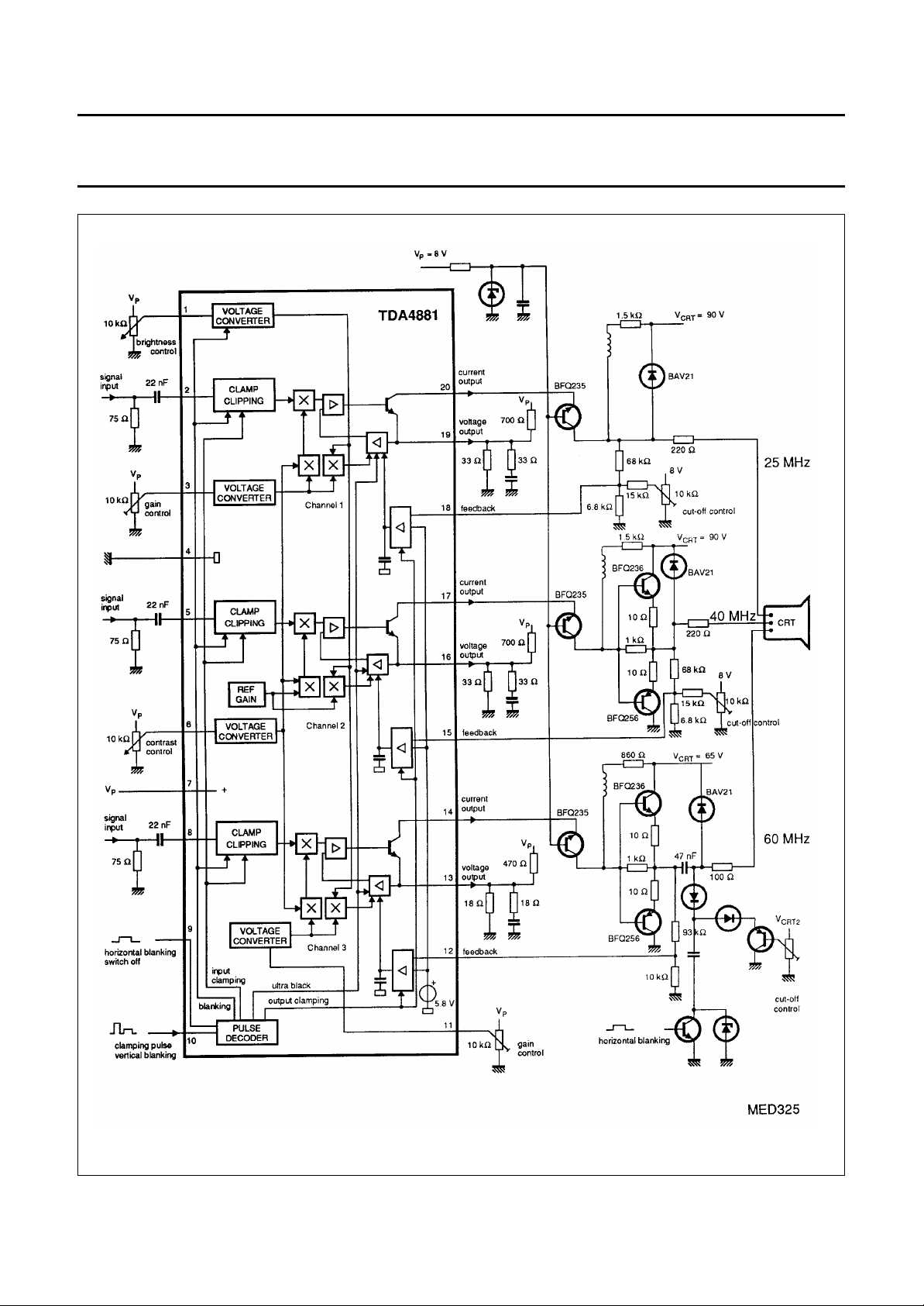
Fig.1 Block diagram and basic application circuit for DC and AC coupling.
November 1992 3
Page 4

Philips Semiconductors Preliminary specification
Advanced monitor video controller TDA4881
PINNING
SYMBOL PIN DESCRIPTION
1 brightness control
2 signal input Channel 1
3 gain control Channel 1
5 signal input Channel 2
6 contrast control
7 supply voltage
8 signal input Channel 3
11 gain control Channel 3
12 feedback Channel 3
13 voltage output Channel 3
14 current output Channel 3
15 feedback Channel 2
16 voltage output Channel 2
17 current output Channel 2
18 feedback Channel 1
19 voltage output Channel 1
20 current output Channel 1
Fig.2 Pin configuration
BR
C
V
I1
G
C1
GND 4 ground
V
I2
C
C
V
P
V
I3
HBL 9 horizontal blanking, switch off
CL 10 input clamping, vertical blanking
G
C3
FB
3
V
O3
I
O3
FB
2
V
O2
I
O2
FB
1
V
O1
I
O1
November 1992 4
Page 5

Philips Semiconductors Preliminary specification
Advanced monitor video controller TDA4881
FUNCTIONAL DESCRIPTION
RGB input signals (0.7 V
the TDA4881 (pins 2, 5 and 8) from a low ohmic source
and are clamped to an internal DC voltage (artificial black
level). Composite signals will not disturb normal
operations because an internal clipping circuit cuts all
signal parts below black level. Channels 1 and 3 have a
maximum total voltage gain of 6 dB (maximum contrast
and maximum individual channel gain), Channel 2 of 4 dB
(maximum contrast and nominal channel gain). With the
nominal channel gain of 1 dB and nominal contrast setting
the nominal black-to-white output amplitude is 0.8 V
DC voltages are used for brightness, contrast and gain
control.
Brightness control
shift of the three channels relative to a reference black
level. For nominal brightness (pin 1 open-circuit) the signal
black level is equal to the reference black level.
Contrast control
affects the three channels simultaneously.
To provide the correct white point, an individual
control
and 3 compared to the reference Channel 2. Gain setting
effects contrast and brightness to achieve correct grey
scale tracking. Each
output (pins 20, 17 and 14) and a voltage output (pins 19,
16 and 13). External cascode transistors reduce power
consumption of the IC and prevent breakdown of the
output transistors. Signal output currents and peaking
characteristics are determined by external components at
the voltage outputs and the video supply. The three
channels have separate internal feedback loops which
ensure large signal linearity and marginal signal distortion
in spite of output transistor thermal VBE variation.
The
only. The input signals have to be at black level during the
clamping pulse and are clamped to an internal artificial
(pins 3 and 11) adjusts the signals of Channels 1
clamping pulse
yields a simultaneous signal black level
is achieved by a voltage at pin 6 and
(pin 10) is used for
) are capacitively coupled into
(p-p)
output stage
provides a current
input clamping
(p-p)
gain
black level. The coupling capacitors are used in this way
for black level storage. Because the threshold for the
clamping pulse is higher than that for vertical blanking (pin
10) the rise and fall times of the clamping pulse have to be
faster than 75 ns/V (1 V to 3.5 V).
The
vertical blanking pulse
voltage (pin 10) is higher than the threshold voltage for
approximately 300 ns but does not exceed the threshold
for the clamping pulse in the time between. During the
vertical blanking pulse the input clamping is disabled to
avoid misclamping in the event of composite input signals.
The input signal is blanked and the artificial black level is
.
inserted instead. Additionally the brightness is internally
set to its nominal value, thus the output signal is at
reference black level. The DC value of the reference black
level will be adjusted by cut-off stabilization.
During
horizontal blanking
reference black level as previously described and
clamping
switch off
ultra black level for screen protection and spot
suppression during V-flyback. Ultra black level is the
lowest possible output voltage (at voltage outputs) and
does not depend on cut-off stabilization.
For
respectively
video signal at the cathode or the coupling capacitor is
divided by an adjustable voltage divider and fed to the
feedback inputs (pins 18, 15 and 12). During horizontal
blanking time this signal is compared with an internal DC
voltage of approximately 5.8 V. Any difference will lead to
a reference black level correction by charging or
discharging the integrated capacitor which stores the
reference black level information between the horizontal
blanking pulses.
is activated. If the voltage at pin 9 exceeds the
threshold the signal is blanked and switched to
cut-off stabilization
black level stabilization
will be detected if the input
(pin 9) the output signal is set to
(DC coupling to the CRT)
(AC coupling) the
output
November 1992 5
Page 6

Philips Semiconductors Preliminary specification
Advanced monitor video controller TDA4881
Fig.3 Internal circuits.
November 1992 6
Page 7

Philips Semiconductors Preliminary specification
Advanced monitor video controller TDA4881
LIMITING VALUES
In accordance with the Absolute Maximum System (IEC 134)
SYMBOL PARAMETER MIN. MAX. UNIT
V
V
V
I
I
P
T
T
T
V
P
i
ext
o
M
tot
stg
amb
j
ESD
supply voltage (pin 7) 0 8.8 V
input voltage range (pins 2, 5 and 8) −0.1 V
P
V
external DC voltage ranges
pins 20, 17 and 14 −0.1 V
P
V
pins 19, 16 and 13 no external voltages
pins 1, 3, 6 and 11 −0.1 V
pin 9 −0.1 V
pin 10 −0.7 V
P
+0.7 V
P
+0.7 V
P
V
average output current (pins 20, 17 and 14) 0 50 mA
peak output current (pins 20, 17 and 14) 0 100 mA
total power dissipation − 1200 mW
storage temperature range −25 +150 °C
operating ambient temperature range 0 +70 °C
junction temperature −25 +150 °C
electrostatic handling for all pins (note 1) −500 +500 V
Note to the Limiting Values
1. Equivalent to discharging a 200 pF capacitor through a 0 Ω series resistor.
THERMAL RESISTANCE
SYMBOL PARAMETER THERMAL RESISTANCE
R
th j-a
from junction to ambient in free air 65 K/W
November 1992 7
Page 8

Philips Semiconductors Preliminary specification
Advanced monitor video controller TDA4881
CHARACTERISTICS
= 8.0 V, T
V
P
SYMBOL PARAMETER CONDITIONS MIN. TYP. MAX. UNIT
V
P
I
P
Video signal inputs
V
l(b-w)
I
2, 5, 8
Brightness control
V
1
R
1
∆V
bl1
V
N1
Contrast control (see note 2)
V
6
I
6
C
v
Tr tracking of RGB signals 2.5 V < V
Gain control
V
3, 11
R
3, 11
G
v
V
N3, N11
Feedback input
V
int
I
18, 15, 12
= +25 °C; all voltages measured to GND (pin 4); unless otherwise specified
amb
supply voltage range (pin 7) 7.2 8.0 8.8 V
supply current (pin 7) − 46 56 mA
input voltage
− 0.7 1.0 V
(black-to-white, pins 2, 5 and 8)
DC current no clamping −0.1 − 0.1 µA
during clamping ±50 −−µA
input voltage range see note 1 1.0 − 6.0 V
input resistance to V
N1
black level voltage change at nominal
gain (pins 19, 16 and 13)
V1= 1.0 V;
V
open-circuit
3, 11
= 6.0 V;
V
1
V
open-circuit
3, 11
− 50 − kΩ
−−80 − mV
− 240 − mV
input voltage for nominal brightness pin 1 open-circuit − 2.25 − V
input voltage range see note 1 1.0 − 6.0 V
current −5 −1 −µA
contrast relative to nominal contrast V6= 6.0 V;
V
open-circuit
3, 11
= 4.5 V;
V
6
V
open-circuit
3, 11
= 1.0 V;
V
6
V
open-circuit
3, 11
V
open-circuit
3, 11
< 6V;
6
− 3 − dB
− 0 − dB
−−20 − dB
− 0 0.5 dB
input voltage range see note 1 1.0 − 6.0 V
input resistance against V
N3, N11
gain relative to nominal gain V6= 4.5 V; V
= 4.5 V; V
V
6
=6V − 2 − dB
3, 11
=1V −−4−dB
3, 11
− 43 − kΩ
input voltage for nominal gain pin 3, 11 open-circuit − 4.6 − V
internal reference voltage see note 3 tbn 5.8 tbn V
output current during output clamping −1.5 −1.0 −0.1 µA
November 1992 8
Page 9

Philips Semiconductors Preliminary specification
Advanced monitor video controller TDA4881
SYMBOL PARAMETER CONDITIONS MIN. TYP. MAX. UNIT
Voltage outputs (pins 19, 16 and 13)
V
O(b-w)
signal output voltage
(black-to-white value)
V
bl
black level voltage during output clamping;
S/N signal-to-noise ratio see note 5 −−44 dB
Frequency response at voltage outputs
G
vf
gain decrease by frequency
response at pins 19, 16 and 13
t
rO
rise time at voltage output
(pins 19, 16 and 13)
V
open; V6= 4.5 V;
3, 11
V
= 0.7 V
l(b-w)
− 0.8 − V
0.3 − 1.0 V
depending on black
level adjustment;
see note 4
during switch-off − 0.1 0.3 V
70 MHz −−−3dB
10% to 90% amplitude;
− 4.5 5.0 ns
input rise time = 1 ns
Current outputs (pins 20, 17 and 14)
l
O(b-w)
V
20-19, 17-16, 14-13
signal current (black-to-white) − 50 − mA
HF saturation of output transistors IO=50mA −−2.0 V
Threshold voltages (see note 7)
V
9
threshold for horizontal blanking
(blanking, output clamping)
threshold for switch-off
(blanking, minimum black level,
no output clamping)
R
9
t
d9
input resistance referenced to ground 50 80 1 10 kΩ
delay between horizontal blanking
input and output signal blanking
V
10
threshold for vertical blanking
(blanking, no input clamping)
threshold for clamping
(input clamping, no blanking)
I
10
t
r,f10
t
w10
t
d10
input current −3 −1 −µA
rise and fall time for clamping pulse transition 1 to 3.5 V;
clamping pulse width V10= 3 V 0.6 −−µs
delay between vertical blanking input
and output signal blanking
with peaking; see note 6 −−100 mA
= 100 mA −−2.2 V
I
O
1.2 1.4 1.6 V
5.8 6.5 6.8 V
− 35 60 ns
see Fig.4 1.2 1.4 1.6 V
see Fig.4 2.6 3.0 3.5 V
−−75 ns/V
see Fig.4
see Fig.4 − 300 − ns
November 1992 9
Page 10

Philips Semiconductors Preliminary specification
Advanced monitor video controller TDA4881
Notes to the characteristics
1. Typical range is 1 to 6 V, the range can be increased (e.g. 0 to 7 V) to slightly increase the control range.
2. Open contrast control pin leads to undefined contrast setting.
3. The internal reference voltage can be measured at pins 18, 15 and 12 during output clamping in closed feedback
loop.
4. Minimum guaranteed control range, the typical minimum black level voltage is 0.1 V.
5. The signal-to-noise ratio is calculated by the formula (frequency range 1 to 70 MHz):
peak-to-peak value of the nominal signal output voltage
---------------------------------------------------------------------------------------------------------------------------------------------------
6. The external RC combinations at pins 19, 16 and 13 enables peak currents during transients.
7. The internal threshold voltages are derived from an internally stabilized voltage. The internal pulses are generated if
the input pulses are higher than the thresholds.
RMS value of the noise output voltage
Fig.4 Timing of pulses at pin 10.
November 1992 10
Page 11

Philips Semiconductors Preliminary specification
Advanced monitor video controller TDA4881
PACKAGE OUTLINE
DIP20: plastic dual in-line package; 20 leads (300 mil)
D
seating plane
L
Z
20
pin 1 index
e
b
SOT146-1
M
E
A
2
A
A
1
w M
b
1
11
E
c
(e )
1
M
H
1
0 5 10 mm
scale
DIMENSIONS (inch dimensions are derived from the original mm dimensions)
A
A
A
UNIT
inches
Note
1. Plastic or metal protrusions of 0.25 mm maximum per side are not included.
max.
mm
OUTLINE
VERSION
SOT146-1
1 2
min.
max.
1.73
1.30
0.068
0.051
IEC JEDEC EIAJ
SC603
b
b
1
0.53
0.38
0.021
0.015
0.36
0.23
0.014
0.009
REFERENCES
cD E e M
(1) (1)
26.92
26.54
1.060
1.045
November 1992 11
6.40
6.22
0.25
0.24
10
(1)
M
e
L
1
3.60
8.25
3.05
7.80
0.14
0.32
0.12
0.31
EUROPEAN
PROJECTION
H
E
10.0
0.2542.54 7.62
8.3
0.39
0.010.10 0.30
0.33
ISSUE DATE
w
92-11-17
95-05-24
Z
max.
2.04.2 0.51 3.2
0.0780.17 0.020 0.13
Page 12

Philips Semiconductors Preliminary specification
Advanced monitor video controller TDA4881
SOLDERING
Introduction
There is no soldering method that is ideal for all IC
packages. Wave soldering is often preferred when
through-hole and surface mounted components are mixed
on one printed-circuit board. However, wave soldering is
not always suitable for surface mounted ICs, or for
printed-circuits with high population densities. In these
situations reflow soldering is often used.
This text gives a very brief insight to a complex technology.
A more in-depth account of soldering ICs can be found in
“IC Package Databook”
our
Soldering by dipping or by wave
The maximum permissible temperature of the solder is
260 °C; solder at this temperature must not be in contact
with the joint for more than 5 seconds. The total contact
DEFINITIONS
Data sheet status
Objective specification This data sheet contains target or goal specifications for product development.
Preliminary specification This data sheet contains preliminary data; supplementary data may be published later.
Product specification This data sheet contains final product specifications.
(order code 9398 652 90011).
time of successive solder waves must not exceed
5 seconds.
The device may be mounted up to the seating plane, but
the temperature of the plastic body must not exceed the
specified maximum storage temperature (T
printed-circuit board has been pre-heated, forced cooling
may be necessary immediately after soldering to keep the
temperature within the permissible limit.
Repairing soldered joints
Apply a low voltage soldering iron (less than 24 V) to the
lead(s) of the package, below the seating plane or not
more than 2 mm above it. If the temperature of the
soldering iron bit is less than 300 °C it may remain in
contact for up to 10 seconds. If the bit temperature is
between 300 and 400 °C, contact may be up to 5 seconds.
stg max
). If the
Limiting values
Limiting values given are in accordance with the Absolute Maximum Rating System (IEC 134). Stress above one or
more of the limiting values may cause permanent damage to the device. These are stress ratings only and operation
of the device at these or at any other conditions above those given in the Characteristics sections of the specification
is not implied. Exposure to limiting values for extended periods may affect device reliability.
Application information
Where application information is given, it is advisory and does not form part of the specification.
LIFE SUPPORT APPLICATIONS
These products are not designed for use in life support appliances, devices, or systems where malfunction of these
products can reasonably be expected to result in personal injury. Philips customers using or selling these products for
use in such applications do so at their own risk and agree to fully indemnify Philips for any damages resulting from such
improper use or sale.
November 1992 12
 Loading...