

Page 1

INTEGRATED CIRCUITS
DATA SH EET
TDA4852
Horizontal and vertical deflection
controller for autosync monitors
Preliminary specification
File under Integrated Circuits, IC02
December 1992
Page 2
Philips Semiconductors Preliminary specification
Horizontal and vertical deflection controller
TDA4852
for autosync monitors
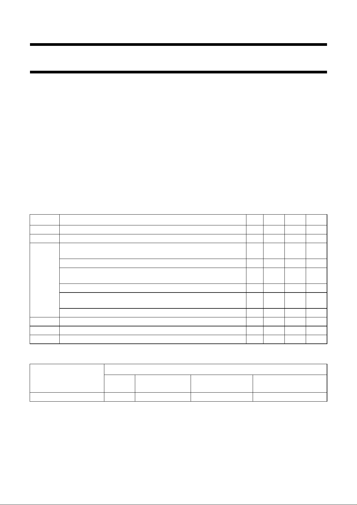
FEATURES
• Low jitter
• All adjustments DC-controllable
• Alignment-free oscillators
• Sync separators for video or horizontal and vertical TTL
sync levels regardless of polarity
• Horizontal oscillator with PLL1 for sync and PLL2 for
flyback
• Constant vertical and E/W amplitude in autosync
operation
• DC-coupling to vertical power amplifier
• Internal supply voltage stabilization with excellent ripple
rejection to ensure stable geometrical adjustments
QUICK REFERENCE DATA
SYMBOL PARAMETER MIN. TYP. MAX. UNIT
V
I
P
V
P
i sync
positive supply voltage (pin 1) 9.2 12 16 V
supply current − 40 − mA
AC-coupled composite video signal with negative-going sync
(peak-to-peak value, pin 9)
sync slicing level − 120 − mV
DC-coupled TTL-compatible horizontal sync signal
(peak-to-peak value, pin 9)
slicing level 1.2 1.4 1.6 V
DC-coupled TTL-compatible vertical sync signal
(peak-to-peak value, pin 10)
slicing level 1.2 1.4 1.6 V
I
I
T
oV
oH
amb
vertical differential output current (peak-to-peak value, pins 5 and 6) − 1 − mA
horizontal sink output current on pin 3 −− 60 mA
operating ambient temperature range 0 − +70 °C
GENERAL DESCRIPTION
The TDA4852 is a monolithic integrated circuit for
economical solutions in autosync monitors. The IC
incorporates the complete horizontal and vertical small
signal processing. In conjunction with TDA4860/61/65, or
TDA8351 (vertical output circuits) the ICs offer an
extremely advanced system solution.
− 1 − V
1.7 −−V
1.7 −−V
ORDERING INFORMATION
EXTENDED
TYPE NUMBER
PINS
PIN
POSITION
TDA4852 20 DIL plastic SOT146
Note
1. SOT146-1; 1996 November 27.
December 1992 2
PACKAGE
MATERIAL CODE
(1)
Page 3
This text is here in white to force landscape pages to be rotated correctly when browsing through the pdf in the Acrobat reader.This text is here in
_white to force landscape pages to be rotated correctly when browsing through the pdf in the Acrobat reader.This text is here inThis text is here in
white to force landscape pages to be rotated correctly when browsing through the pdf in the Acrobat reader. white to force landscape pages to be ...
December 1992 3
Philips Semiconductors Preliminary specification
Horizontal and vertical deflection controller
for autosync monitors
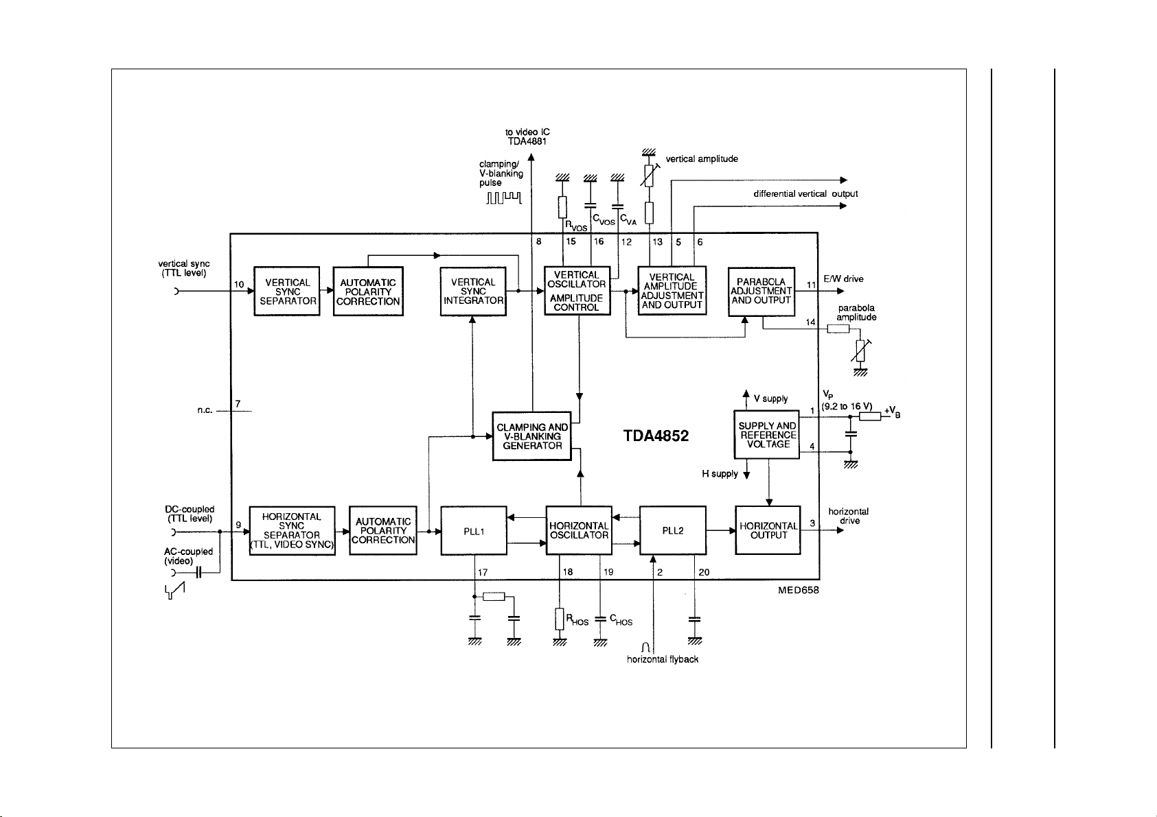
Fig.1 Block diagram.
TDA4852
Page 4
Philips Semiconductors Preliminary specification
Horizontal and vertical deflection controller
for autosync monitors
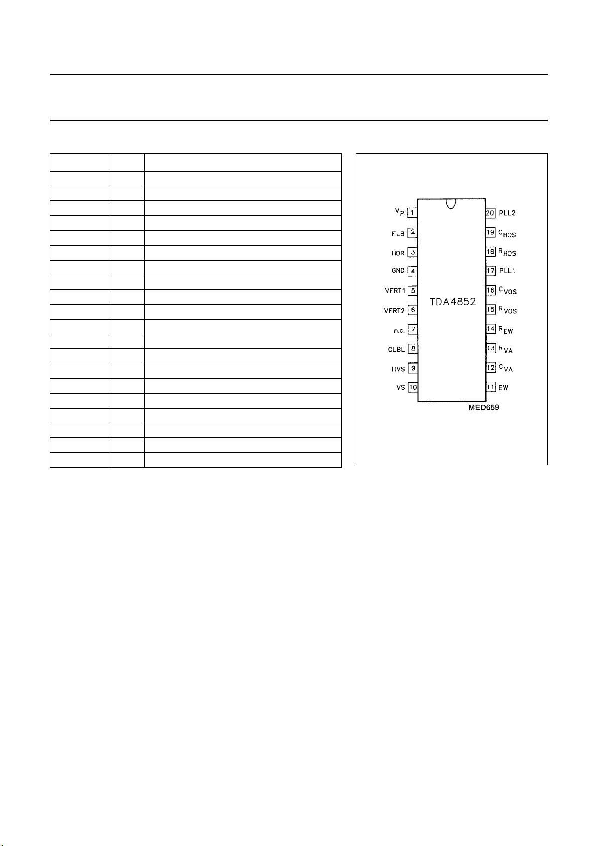
PINNING
SYMBOL PIN DESCRIPTION
V
P
FLB 2 horizontal flyback input
HOR 3 horizontal output
GND 4 ground (0 V)
VERT1 5 vertical output 1; negative-going sawtooth
VERT2 6 vertical output 2; positive-going sawtooth
n.c. 7 not connected
CLBL 8 clamping/blanking pulse output
HVS 9 horizontal sync/video input
VS 10 vertical sync input
EW 11 E/W output (parabola to driver stage)
C
VA
R
VA
R
EW
R
VOS
C
VOS
PLL1 17 PLL1 phase
R
HOS
C
HOS
PLL2 20 PLL2 phase
1 positive supply voltage
12 capacitor for amplitude control
13 vertical amplitude adjustment input
14 E/W amplitude adjustment input (parabola)
15 vertical oscillator resistor
16 vertical oscillator capacitor
18 horizontal oscillator resistor
19 horizontal oscillator capacitor
TDA4852
Fig.2 Pin configuration.
December 1992 4
Page 5

Philips Semiconductors Preliminary specification
Horizontal and vertical deflection controller
for autosync monitors
FUNCTIONAL DESCRIPTION
Horizontal sync separator and
polarity correction
An AC-coupled video signal or a
DC-coupled TTL sync signal (H only
or composite sync) is input on pin 9.
Video signals are clamped with top
sync on 1.28 V, and are sliced at
1.4 V. This results in a fixed absolute
slicing level of 120 mV related to top
sync. DC-coupled TTL sync signals
are also sliced at 1.4 V, however with
the clamping circuit in current
limitation. The polarity of the
separated sync is detected by internal
integration of the signal, then the
polarity is corrected. The corrected
sync is input signal for the vertical
sync integrator and the PLL1 stage.
Vertical sync separator, polarity
correction and vertical sync
integrator
DC-coupled vertical TTL sync signals
may be applied to pin 10. They are
sliced at 1.4 V. The polarity of the
separated sync is detected by internal
integration, then the polarity is
corrected. If pin 10 is not used, it must
be connected to ground. The
separated V
signal from pin 10, or
i sync
the integrated composite sync signal
from pin 9 (TTL or video) triggers
directly the vertical oscillator.
Clamping and V-blanking
generator
A combined clamping and V-blanking
pulse is available on pin 8 (suitable for
the video pre-amplifier TDA4881).
The lower level of 1.9 V is the
blanking signal derived from the
vertical blanking pulse from the
internal vertical oscillator.
Vertical blanking starts with vertical
sync and stops at the begin of vertical
scan. By this, an optimum blanking is
achieved. The upper level of 5.4 V is
the horizontal clamping pulse with an
internally fixed pulse width of 0.8 µs.
A monoflop, which is triggered by the
trailing edge of the horizontal sync
pulse, generates this pulse. If
composite sync is applied, one
clamping pulse per H-period is
generated during V-sync. The phase
of the clamping pulse may change
during V-sync (see Fig.8).
PLL1 phase detector
The phase detector is a standard type
using switched current sources. The
middle of the sync is compared with a
fixed point of the oscillator sawtooth
voltage. The PLL filter is connected to
pin 17. If composite sync is applied,
the disturbed control voltage is
corrected during V-sync (see Fig.8).
Horizontal oscillator
This oscillator is of the relaxation type
and requires a fixed capacitor of
10 nF at pin 19. By changing the
current into pin 18 the whole
frequency range from 13 to 100 kHz
can be covered. The current can be
generated either by a frequency to
voltage converter or by a resistor.
A frequency adjustment may also be
added if necessary.
The PLL1 control voltage at pin 17
modulates via a buffer stage the
oscillator thresholds. A high DC-loop
gain ensures a stable phase
relationship between horizontal sync
and line flyback pulses.
PLL2 phase detector
This phase detector is similar to the
PLL1 phase detector. Line flyback
signals (pin 2) are compared with a
fixed point of the oscillator sawtooth
voltage. Delays in the horizontal
deflection circuit are compensated by
adjusting the phase relationship
between horizontal sync and
horizontal output pulses. A certain
amount of phase adjustment is
possible by injecting a DC current
from an external source into the PLL2
filter capacitor at pin 20.
TDA4852
Horizontal driver
This open-collector output stage
(pin 3) can directly drive an external
driver transistor. The saturation
voltage is less than 300 mV at 20 mA.
To protect the line deflection
transistor, the horizontal output stage
does not conduct for
V
< 6.4 V (pin 1).
P
Vertical oscillator and amplitude
control
This stage is designed for fast
stabilization of the vertical amplitude
after changes in sync conditions. The
free-running frequency f
determined by the values of R
. The recommended values
C
VOS
should be altered marginally only to
preserve the excellent linearity and
noise performance. The vertical drive
currents I
value of R
and I6are in relation to the
5
. Therefore, the
VOS
oscillator frequency must be
determined only by C
f
=
-----------------------------------------------------
0
10.8 R
1
××
VOSCVOS
To achieve a stabilized amplitude the
free-running frequency f
adjustment) must be lower than the
lowest occurring sync frequency. The
following contributions can be
assumed:
minimum frequency
offset between f0and the
lowest trigger frequency 10%
spread of IC ±3%
spread of R (22 kΩ) ±1%
spread of C (0.1 µF) ±5%
Result: f
50
-----------
0
1.19
(for 50 to 110 Hz application)
VOS
Hz=42Hz=
is
0
VOS
on pin 16.
(without
0
19%
and
December 1992 5
Page 6
Philips Semiconductors Preliminary specification
Horizontal and vertical deflection controller
TDA4852
for autosync monitors
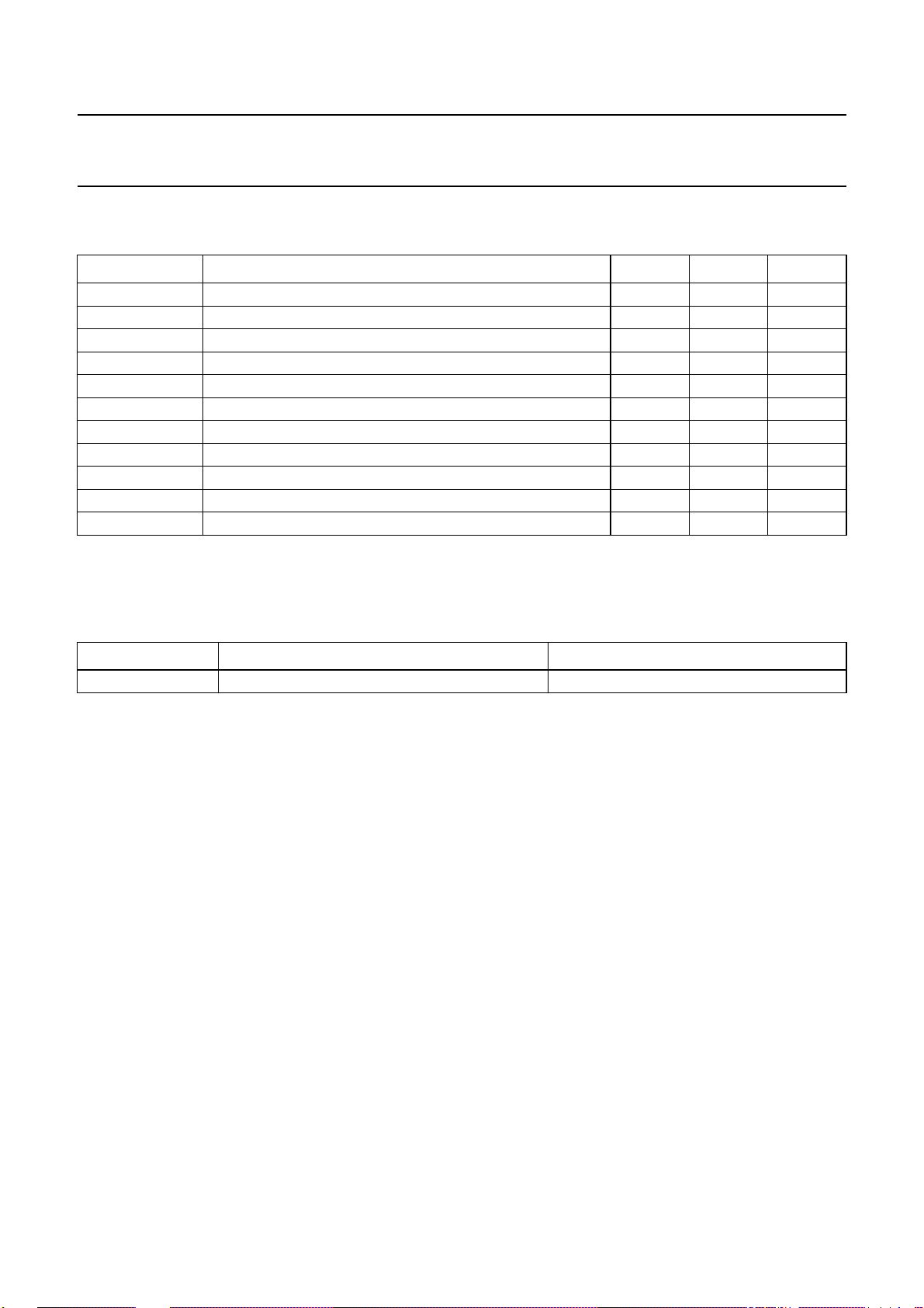
LIMITING VALUES
In accordance with the Absolute Maximum Rating System (IEC 134)
SYMBOL PARAMETER MIN. MAX. UNIT
V
P
V
3
V
8
V
n
I
2
I
3
I
8
T
stg
T
amb
T
j
V
ESD
Note to the Limiting Values
1. Equivalent to discharging a 200 pF capacitor through a 0 Ω series resistor.
supply voltage (pin 1) −0.5 16 V
voltage on pin 3 −0.5 16 V
voltage on pin 8 −0.5 7 V
voltage on pins 5, 6, 9, 10, 13, 14 and 18 −0.5 6.5 V
current on pin 2 −±10 mA
current on pin 3 − 100 mA
current on pin 8 −−10 mA
storage temperature range −55 +50 °C
operating ambient temperature range 0 70 °C
maximum junction temperature 0 +150 °C
electrostatic handling for all pins (note 1) −±400 V
THERMAL RESISTANCE
SYMBOL PARAMETER THERMAL RESISTANCE
R
th j-a
from junction to ambient in free air 65 K/W
December 1992 6
Page 7
Philips Semiconductors Preliminary specification
Horizontal and vertical deflection controller
TDA4852
for autosync monitors
CHARACTERISTICS
V
= 12 V; T
P
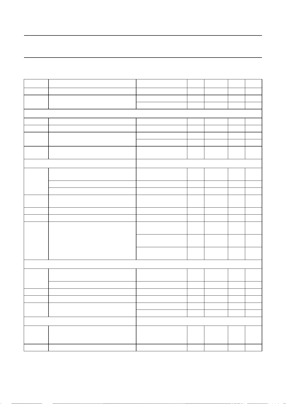
SYMBOL PARAMETER CONDITIONS MIN. TYP. MAX. UNIT
V
P
I
P
Internal reference voltage
V
ref
TC temperature coefficient T
PSRR power supply ripple rejection f = 1 kHz sinewave 60 75 − dB
V
P
Composite sync input (AC-coupled)
v
i sync
R
S
r
9
I
9
t
int
=+25 °C; measurements taken in Fig.3 unless otherwise specified.
amb
positive supply voltage (pin 1) 9.2 12 16 V
supply current I18= −1.05 mA − 36 44 mA
I
= −3.388 mA − 40 49 mA
18
internal reference voltage 6.0 6.25 6.5 V
= +20 to +100 °C −− ±90 10−6/K
amb
f = 1 MHz sinewave 25 35 − dB
supply voltage (pin 1) to ensure all
9.2 − 16 V
internal reference voltages
V
= 5 V
10
sync amplitude of video input signal
sync on green − 300 − mV
(pin 9)
top sync clamping level 1.1 1.28 1.5 V
slicing level above top sync level R
allowed source resistance for 7%
= 50 Ω 90 120 150 mV
S
V
> 200 mV −− 1.5 kΩ
i sync
duty factor
differential input resistance during sync − 80 −Ω
charging current of coupling capacitor V9> 1.5 V 1.3 2 3 µA
vertical sync integration time to
generate vertical trigger pulse
fH= 31 kHz;
I18= −1.050 mA
= 64 kHz;
f
H
710 13µs
3.5 5 6.5 µs
I18= −2.169 mA
f
= 100 kHz;
H
2.5 3.4 4.5 µs
I18= −3.388 mA
Horizontal sync input (DC-coupled, TTL-compatible)
V
i sync
sync input signal
(peak-to-peak value, pin 9)
slicing level 1.2 1.4 1.6 V
t
p
t
, t
r
f
I
9
minimum pulse width 700 −−ns
rise time and fall time 10 − 500 ns
input current V9= 0.8 V −− −200 µA
V
Automatic horizontal polarity switch
t
p H/tH
horizontal sync pulse width related to t
H-sync on pin 9
H
(duty factor for automatic polarity
correction)
t
p
delay time for changing sync polarity 0.3 − 1.8 ms
December 1992 7
1.7 −−V
= 5.5 V −− 10 µA
9
−− 30 %
Page 8
Philips Semiconductors Preliminary specification
Horizontal and vertical deflection controller
TDA4852
for autosync monitors
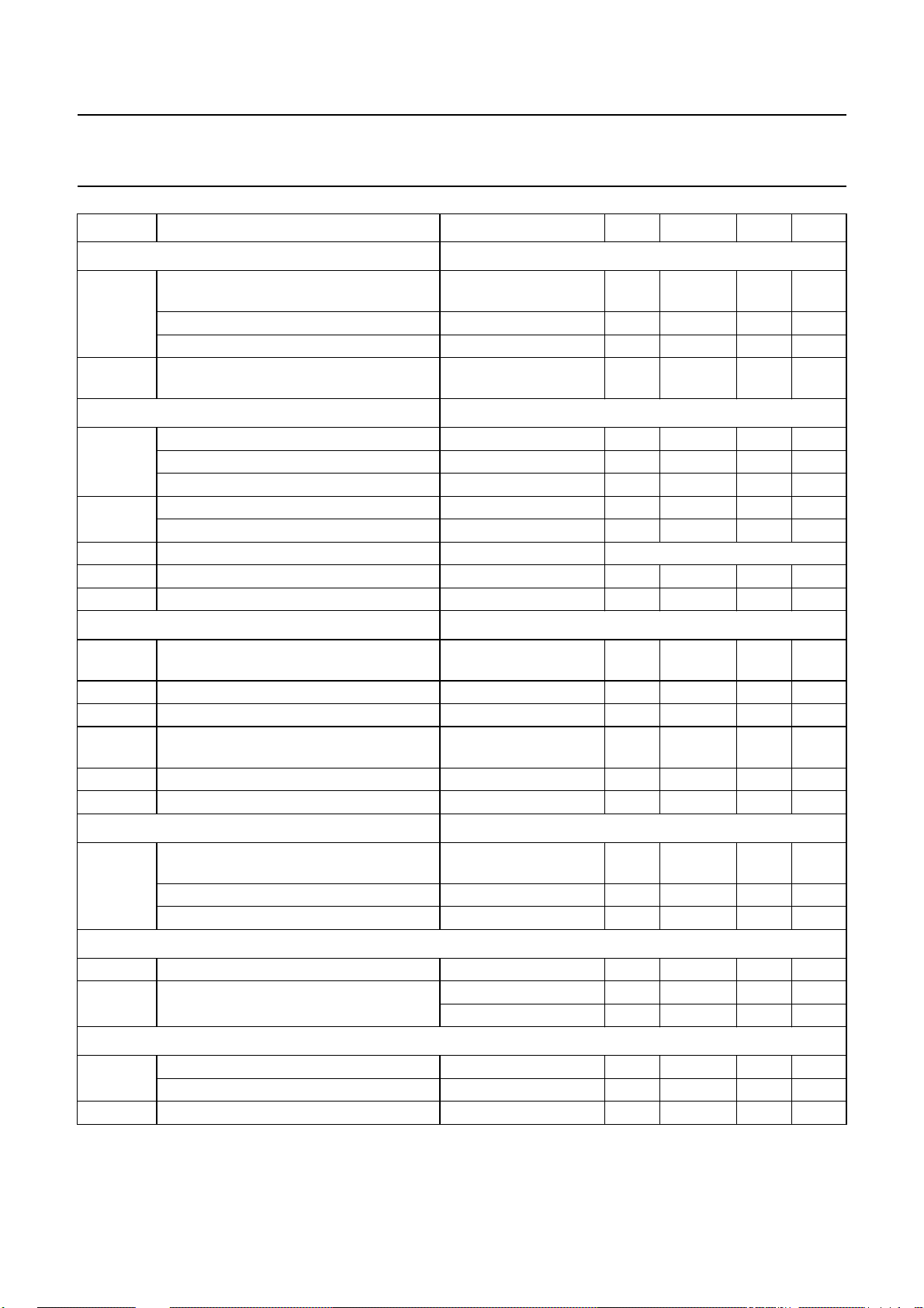
SYMBOL PARAMETER CONDITIONS MIN. TYP. MAX. UNIT
Vertical sync input (DC-coupled, TTL-compatible)
V
i sync
sync input signal
(peak-to-peak value, pin 10)
slicing level 1.2 1.4 1.6 V
I
t
10
p V
input current 0 < V10< 5.5 V −− ±10 µA
maximum vertical sync pulse width for
automatic vertical polarity switch
Horizontal clamping / blanking generator output
V
8
output voltage LOW −− 0.9 V
blanking output voltage internal V blanking 1.6 1.9 2.2 V
clamping output voltage H-sync on pin 9 5.15 5.4 5.65 V
I
8
internal sink current for all output levels H and V scanning 2.3 2.9 3.5 mA
external load current −− −3.0 mA
t
8
t
clp
clamping pulse start with end of H-sync
clamping pulse width V8= 3 V 0.6 0.8 1.0 µs
S steepness of rise and fall times − 60 75 ns/V
Vertical oscillator
f
0
f
v
V
15
t
d
vertical free-running frequency R15= 22 kΩ;
nominal vertical sync range no f0adjustment 50 − 110 Hz
voltage on pin 15 R15= 22 kΩ 2.8 3.0 3.2 V
delay between sync pulse and start of
vertical scan
I
12
C
12
control current for amplitude control −±200 −µA
capacitor for amplitude control −− 0.18 µF
Vertical differential output
I
o
differential output current between
pins 5 and 6 (peak-to-peak value)
maximum offset-current error I
maximum linearity error −− ±1.5 %
V-sync on pin 10
1.7 −−V
−− 300 µs
Fig.6
V
= 6.25 V
ref
− 42 − Hz
C16= 0.1 µF
measured on pin 8 240 300 360 µs
Fig.7
mode 3; I13>−135 µA;
0.9 1.0 1.1 mA
R15= 22 kΩ
= 1 mA −− ±2.5 %
o
Vertical amplitude adjustment (in percentage of output signal)
V
13
I
13
input voltage − 5.0 − V
adjustment current I
o max
I
o min
Horizontal comparator PLL1
V
17
upper control voltage limitation − 5.9 − V
lower control voltage limitation − 5.1 − V
I
17
control current Fig.6 −±0.083I18− mA
December 1992 8
(100%) −110 −120 −135 µA
(typically 58%) − 0 −µA
Page 9
Philips Semiconductors Preliminary specification
Horizontal and vertical deflection controller
TDA4852
for autosync monitors
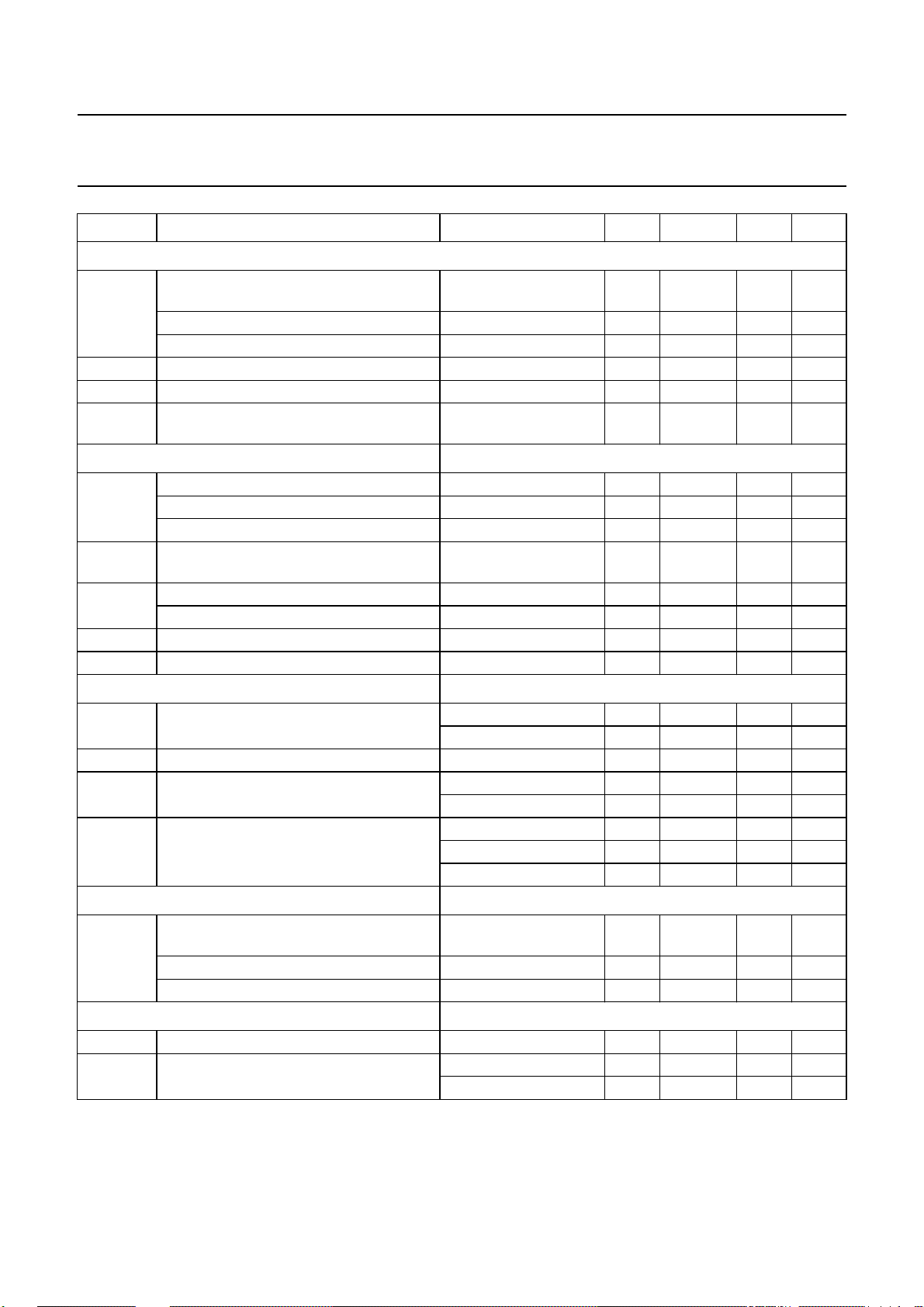
SYMBOL PARAMETER CONDITIONS MIN. TYP. MAX. UNIT
Horizontal oscillator
f
osc
centre frequency R18= 2.4 kΩ (pin 18);
deviation of centre frequency −− ±3%
temperature coefficient 0 +200 +300 10
ϕ
I
V
H/tH
18
18
relative holding/catching range ±6 ±6.5 ±7.3 %
external oscillator current −0.5 −−4.3 mA
voltage at reference current input
(pin18)
Horizontal PLL2
V
2
upper clamping level of flyback input I2= 6 mA − 5.5 − V
lower clamping level of flyback input I
H-flyback slicing level − 3.0 − V
td/t
H
delay between middle of sync and
middle of H-flyback related to t
V
20
upper control voltage limitation − 6.2 − V
lower control voltage limitation − 4.8 − V
I
20
∆t/t
H
control current −±0.083I18−µA
PLL2 control range related to t
Horizontal output (open-collector)
V
t
p/tH
V
3
P
output voltage LOW I3= 20 mA −− 0.3 V
tHduty factor 42 45 48 %
threshold to activate under voltage
protection
∆t
H
jitter of horizontal output f = 31 kHz −− 3.5 ns
E/W output
V
11
bottom output signal during mid-scan
(pin 11)
top output signal during flyback 4.2 4.5 4.8 V
temperature coefficient of output signal −− 250 10−6/K
E/W amplitude adjustment (parabola)
V
14
I
14
input voltage (pin 14) − 5.0 − V
adjustment current 100% parabola −110 −120 −135 µA
C19= 10 nF (pin 19)
Fig.6
= −1 mA −−0.75 − V
2
H
H
Fig.6
I
= 60 mA −− 0.8 V
3
horizontal output off − 5.6 − V
horizontal output on − 5.8 − V
f = 64 kHz −− 1.9 ns
f = 100 kHz −− 1.2 ns
note 1
internally stabilized 1.05 1.2 1.35 V
Fig.7
typically 28% parabola − 0 −µA
− 31.45 − kHz
−6
2.35 2.5 2.65 V
− 3.0 − %
30 −−%
/K
Note to the characteristics
1. Parabola amplitude does not track with vertical amplitude adjustment. Tracking can be achieved by a resistor from
vertical amplitude potentiometer to pin 14.
December 1992 9
Page 10
Philips Semiconductors Preliminary specification
Horizontal and vertical deflection controller
for autosync monitors
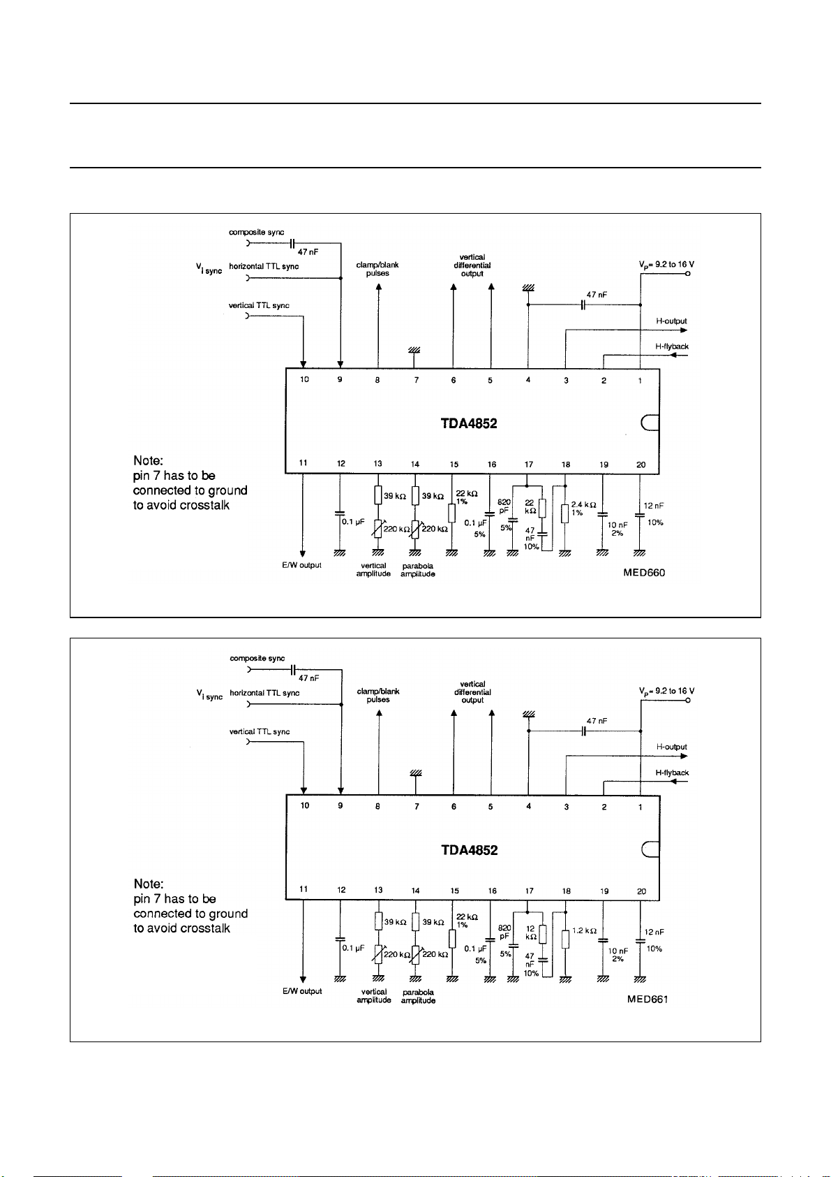
APPLICATION INFORMATION
Note:
pin 7 has to be
connected to ground
to avoid crosstalk
from pin 8 to pin 6.
TDA4852
Note:
pin 7 has to be
connected to ground
to avoid crosstalk
from pin 8 to pin 6.
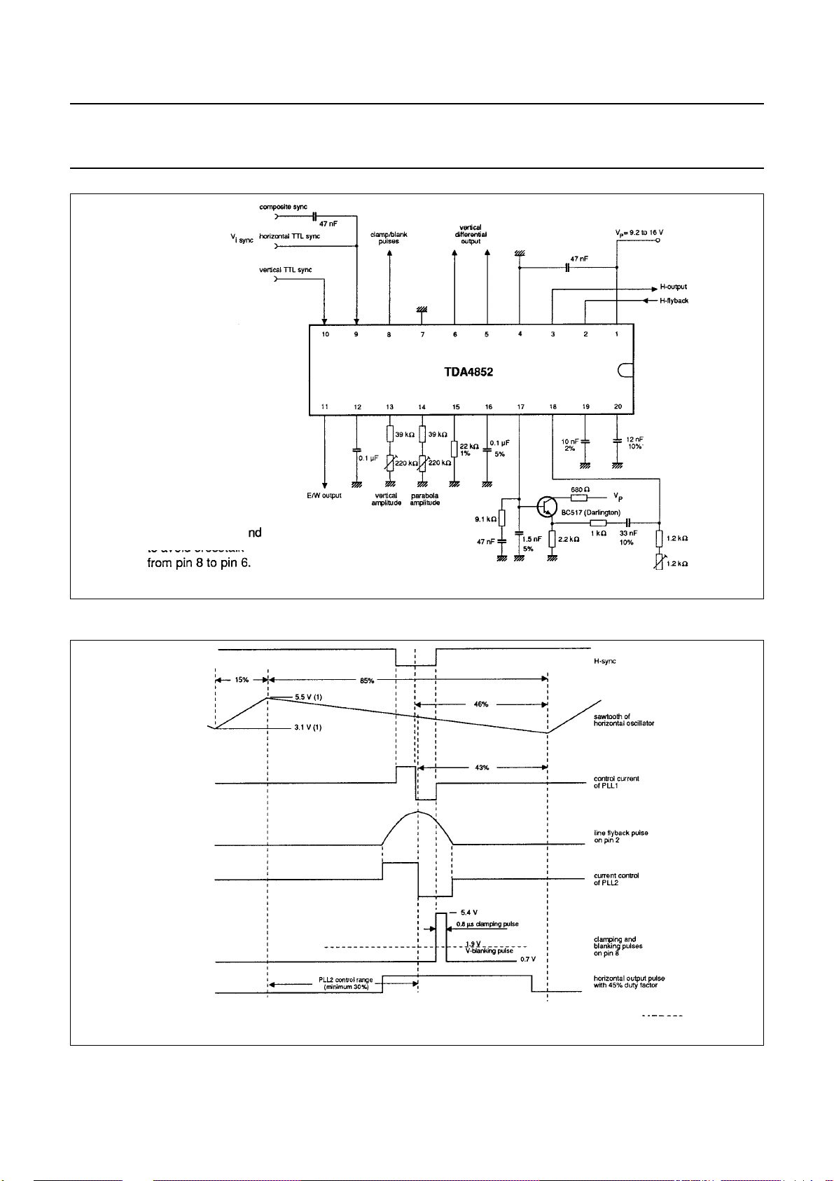
Fig.3 Application circuit for 31.45 kHz.
Fig.4 Application circuit for 64 kHz.
December 1992 10
Page 11
Philips Semiconductors Preliminary specification
Horizontal and vertical deflection controller
for autosync monitors
Note:
pin 7 has to be
connected to ground
to avoid crosstalk
from pin 8 to pin 6.
TDA4852
Fig.5 Application circuit for 31 to 64 kHz.
(1) tracks with PLL1 control voltage at pin 17
Fig.6 Horizontal timing diagram.
December 1992 11
Page 12
Philips Semiconductors Preliminary specification
Horizontal and vertical deflection controller
for autosync monitors
TDA4852
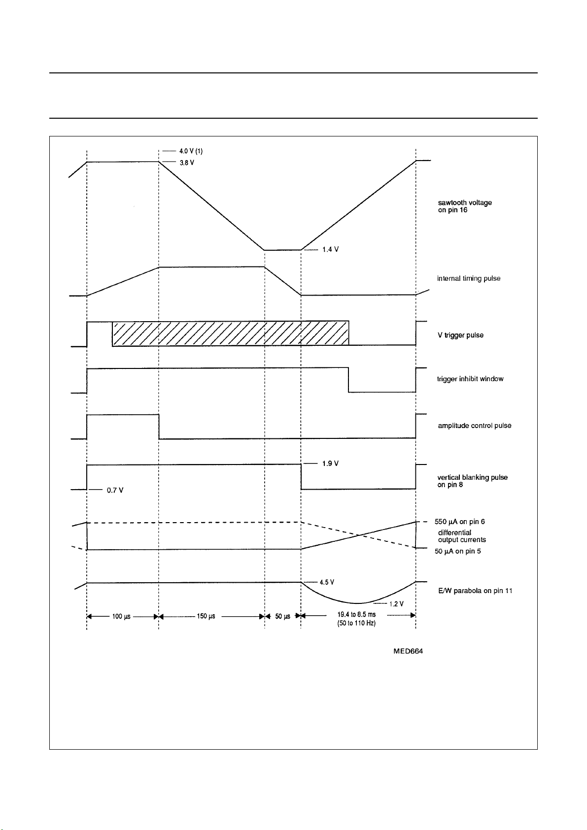
(1) for free-running oscillator
Fig.7 Vertical and E/W timing diagram.
December 1992 12
Page 13
This text is here in white to force landscape pages to be rotated correctly when browsing through the pdf in the Acrobat reader.This text is here in
_white to force landscape pages to be rotated correctly when browsing through the pdf in the Acrobat reader.This text is here inThis text is here in
white to force landscape pages to be rotated correctly when browsing through the pdf in the Acrobat reader. white to force landscape pages to be ...
December 1992 13
Philips Semiconductors Preliminary specification
Horizontal and vertical deflection controller
for autosync monitors
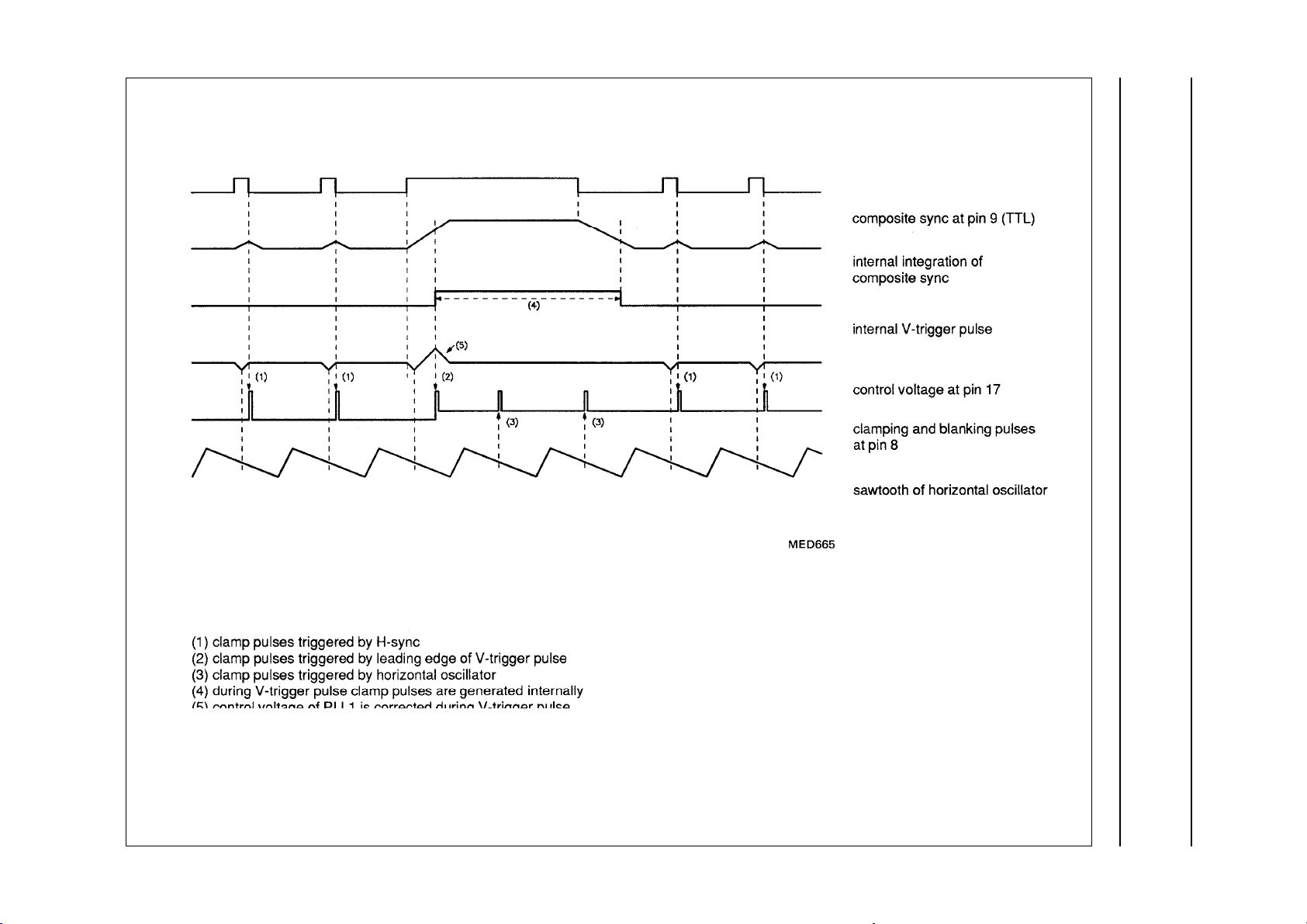
(1) clamp pulses triggered by H-sync
(2) clamp pulses triggered by leading edge of V-trigger pulse
(3) clamp pulses triggered by horizontal oscillator
(4) during V-trigger pulse clamp pulses are generated internally
(5) control voltage of PLL1 is corrected during V-trigger pulse
Fig.8 Pulse diagram for composite sync applications (showing reduced influence of V-sync on H-phase and drive pulses for F/V converters).
TDA4852
Page 14
This text is here in white to force landscape pages to be rotated correctly when browsing through the pdf in the Acrobat reader.This text is here in
_white to force landscape pages to be rotated correctly when browsing through the pdf in the Acrobat reader.This text is here inThis text is here in
white to force landscape pages to be rotated correctly when browsing through the pdf in the Acrobat reader. white to force landscape pages to be ...
December 1992 14
Philips Semiconductors Preliminary specification
Horizontal and vertical deflection controller
for autosync monitors
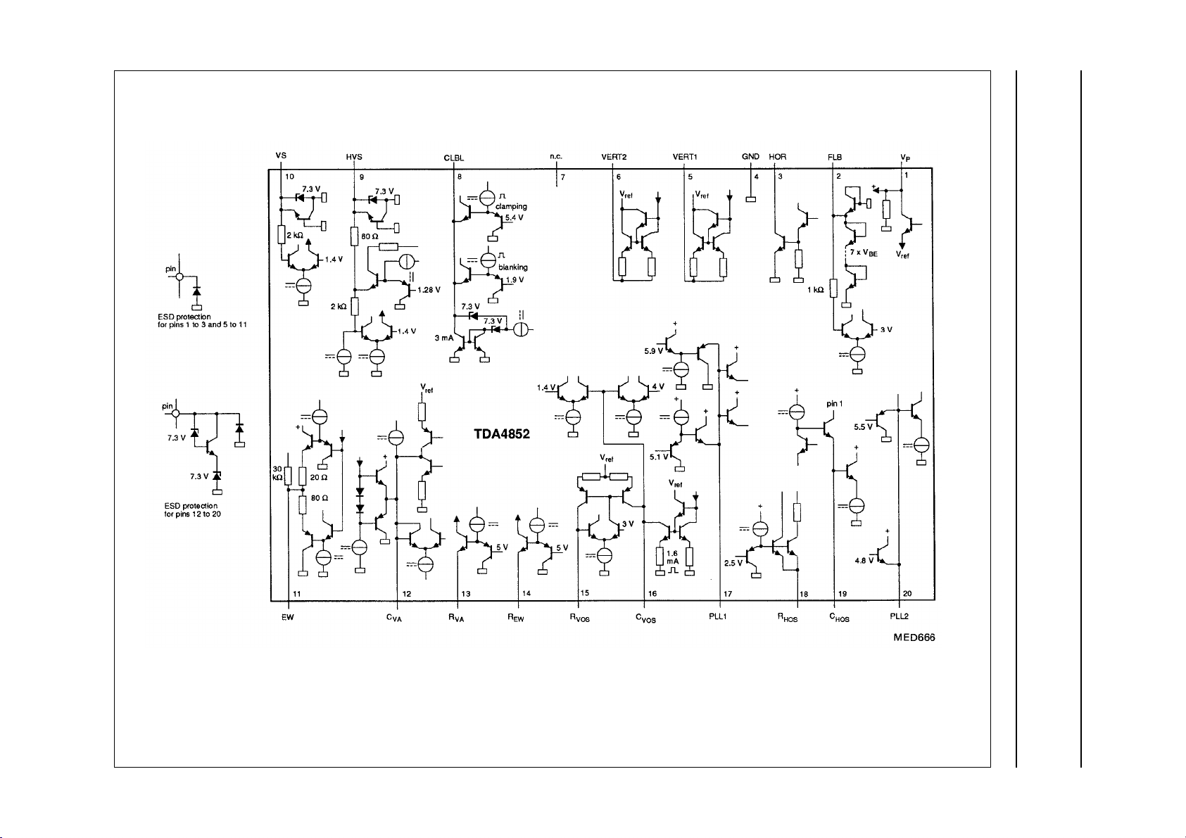
Fig.9 Internal circuits.
TDA4852
Page 15
Philips Semiconductors Preliminary specification
Horizontal and vertical deflection controller
for autosync monitors
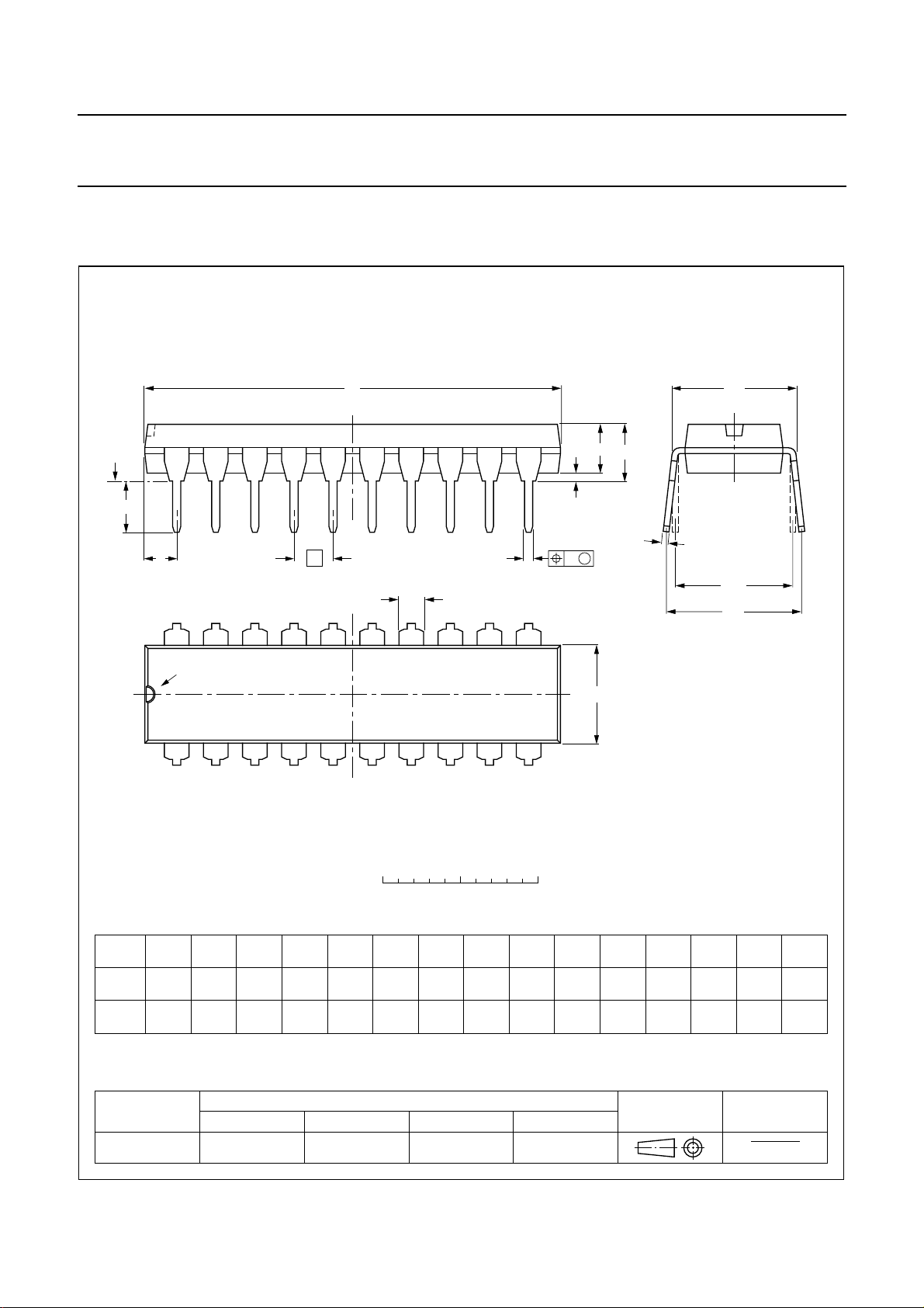
PACKAGE OUTLINE
DIP20: plastic dual in-line package; 20 leads (300 mil)
D
seating plane
L
Z
20
e
b
TDA4852
SOT146-1
M
E
A
2
A
A
1
w M
b
1
11
c
(e )
1
M
H
pin 1 index
1
0 5 10 mm
scale
DIMENSIONS (inch dimensions are derived from the original mm dimensions)
A
A
A
UNIT
inches
Note
1. Plastic or metal protrusions of 0.25 mm maximum per side are not included.
max.
mm
OUTLINE
VERSION
SOT146-1
1 2
min.
max.
1.73
1.30
0.068
0.051
IEC JEDEC EIAJ
b
b
1
0.53
0.38
0.021
0.015
0.36
0.23
0.014
0.009
REFERENCES
cD E e M
(1) (1)
26.92
26.54
1.060
1.045
SC603
6.40
6.22
0.25
0.24
E
10
(1)
M
e
L
1
3.60
8.25
3.05
7.80
0.14
0.32
0.12
0.31
EUROPEAN
PROJECTION
H
E
10.0
0.2542.54 7.62
8.3
0.39
0.010.10 0.30
0.33
ISSUE DATE
w
92-11-17
95-05-24
Z
max.
2.04.2 0.51 3.2
0.0780.17 0.020 0.13
December 1992 15
Page 16
Philips Semiconductors Preliminary specification
Horizontal and vertical deflection controller
for autosync monitors
SOLDERING
Introduction
There is no soldering method that is ideal for all IC
packages. Wave soldering is often preferred when
through-hole and surface mounted components are mixed
on one printed-circuit board. However, wave soldering is
not always suitable for surface mounted ICs, or for
printed-circuits with high population densities. In these
situations reflow soldering is often used.
This text gives a very brief insight to a complex technology.
A more in-depth account of soldering ICs can be found in
our
“IC Package Databook”
Soldering by dipping or by wave
The maximum permissible temperature of the solder is
260 °C; solder at this temperature must not be in contact
DEFINITIONS
(order code 9398 652 90011).
TDA4852
with the joint for more than 5 seconds. The total contact
time of successive solder waves must not exceed
5 seconds.
The device may be mounted up to the seating plane, but
the temperature of the plastic body must not exceed the
specified maximum storage temperature (T
printed-circuit board has been pre-heated, forced cooling
may be necessary immediately after soldering to keep the
temperature within the permissible limit.
Repairing soldered joints
Apply a low voltage soldering iron (less than 24 V) to the
lead(s) of the package, below the seating plane or not
more than 2 mm above it. If the temperature of the
soldering iron bit is less than 300 °C it may remain in
contact for up to 10 seconds. If the bit temperature is
between 300 and 400 °C, contact may be up to 5 seconds.
stg max
). If the
Data sheet status
Objective specification This data sheet contains target or goal specifications for product development.
Preliminary specification This data sheet contains preliminary data; supplementary data may be published later.
Product specification This data sheet contains final product specifications.
Limiting values
Limiting values given are in accordance with the Absolute Maximum Rating System (IEC 134). Stress above one or
more of the limiting values may cause permanent damage to the device. These are stress ratings only and operation
of the device at these or at any other conditions above those given in the Characteristics sections of the specification
is not implied. Exposure to limiting values for extended periods may affect device reliability.
Application information
Where application information is given, it is advisory and does not form part of the specification.
LIFE SUPPORT APPLICATIONS
These products are not designed for use in life support appliances, devices, or systems where malfunction of these
products can reasonably be expected to result in personal injury. Philips customers using or selling these products for
use in such applications do so at their own risk and agree to fully indemnify Philips for any damages resulting from such
improper use or sale.
December 1992 16
 Loading...