

Page 1

INTEGRATED CIRCUITS
DATA SH EET
TDA4651
Multistandard colour decoder with
negative colour difference output
signals
Preliminary specification
File under Integrated Circuits, IC02
August 1993
Page 2

Philips Semiconductors Preliminary specification
Multistandard colour decoder with negative
colour difference output signals
FEATURES
Identifies and demodulates PAL,
SECAM, NTSC 3.58 and NTSC 4.43
chrominance signals with:
• Gain controlled chrominance
amplifier
• ACC demodulation controlled by
system scanning
• Internal colour difference signal
output filters to remove the residual
subcarrier
• PAL / NTSC demodulation
– H (burst) and V blanking
– PAL switch (disabled for NTSC)
– NTSC phase shift (disabled for
PAL)
– PLL-controlled reference
oscillator
– two reference oscillator crystals
on separate pins with automatic
switching
– quadrature demodulator with
subcarrier reference
• SECAM demodulation
– limiter amplifier
– quadrature demodulator with a
single external reference tuned
circuit
– alternate line blanking, H and V
blanking
– de-emphasis
• Identification
– automatic standard identification
by sequential inquiry
– secure SECAM identification at
50 Hz only, with PAL priority
– four switched outputs for
chrominance filter selection and
display control
– external service switch for
oscillator adjustment
GENERAL DESCRIPTION
The TDA4651 is a monolithic integrated multistandard colour decoder for PAL,
SECAM and NTSC (3.58 and 4.43 MHz) with negative colour difference output
signals. The colour difference output signals are fed to the TDA4661, switched
capacitor delay line.
QUICK REFERENCE DATA
SYMBOL PARAMETER CONDITIONS MIN. TYP. MAX. UNIT
V
P
positive
supply voltage
(pin 13)
I
P
supply current
(pin 13)
V
i(p-p)
chrominance
input voltage
(pin 15)
(peak-to-peak
value)
Colour difference output signals (see note 2)
V
1(p-p)
−(R−Y) output
(peak-to-peak
value)
V
3(p-p)
−(B−Y) output
(peak-to-peak
value)
Notes to quick reference data
1. Within 3 dB output voltage deviation.
2. Burst key width for PAL 4.3 µs, for NTSC 3.6 µs
Burst width for PAL and NTSC 2.25 µs, ratio burst-chrominance-amplitude
1/2.2.
ORDERING INFORMATION
EXTENDED
TYPE NUMBER
PINS
TDA4651 28 DIL plastic SOT117
TDA4651WP 28 PLCC plastic SOT261CG
Note
1. SOT117-1; 1996 November 25.
2. SOT261-2; 1996 November 25.
TDA4651
10.8 12 13.2 V
− 60 − mA
see note 1 20 200 400 mV
PAL 442 525 624 mV
NTSC 370 440 523 mV
SECAM 883 1050 1248 mV
PAL 559 665 791 mV
NTSC 468 557 662 mV
SECAM 1119 1330 1581 mV
PACKAGE
PIN
POSITION
MATERIAL CODE
(1)
(2)
August 1993 2
Page 3
Philips Semiconductors Preliminary specification
Multistandard colour decoder with negative
colour difference output signals
TDA4651
August 1993 3
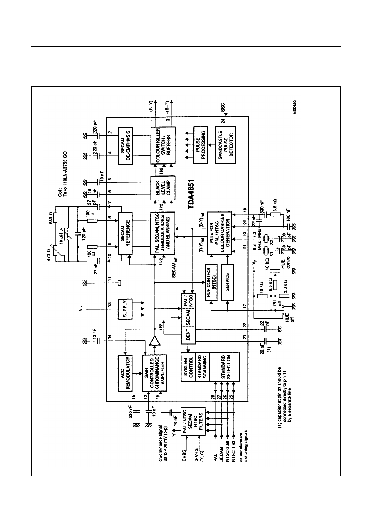
Fig.1 Block diagram.
Page 4
Philips Semiconductors Preliminary specification
Multistandard colour decoder with negative
colour difference output signals
PINNING
SYMBOL PIN DESCRIPTION
−(R−Y)
o
−(R−Y)
DE
−(B−Y)
o
−(B−Y)
DE
−(B−Y)
CL
−(R−Y)
CL
SEC
REF
GND 11 ground
CHR
2
V
P
C
DC
1 −(R−Y) output
2(R−Y) de-emphasis
3 −(B−Y) output
4(B−Y) de-emphasis
5(B−Y) clamping
6(R−Y) clamping
7 SECAM reference tuned circuit
8
9
10
12 DC for ACC
13 supply voltage
14 DC feedback
TDA4651
CHR
1
C
ACC
HUE 17 hue control
PLL 18 PLL time constant
OSC1 19 input for 7.15 MHz oscillator
C
PLL
OSC2 21 input for 8.86 MHz oscillator
N
IDENT
P
IDENT
SSC 24 super sandcastle pulse input
N
01
N
02
SEC
0
PAL
0
15 chrominance input
16 automatic colour control
20 PLL DC reference
22 NTSC identification
23 PAL/SECAM identification
25 NTSC (4.43 MHz) identification
26 NTSC (3.58 MHz) identification
27 SECAM identification
28 PAL identification
Fig.2 Pin configuration for DIL
package.
August 1993 4
Fig.3 Pin configuration for PLCC package.
Page 5

Philips Semiconductors Preliminary specification
Multistandard colour decoder with negative
colour difference output signals
FUNCTIONAL DESCRIPTION
The IC (see block diagram Fig.1)
contains all functions required for the
identification and demodulation of
PAL, SECAM, NTSC 4.43 MHz and
NTSC 3.58 MHz signals. When an
unknown signal is fed into the input,
the circuit has to identify the standard
of the signal; to achieve this it has to
switch on successively the
appropriate input filter, crystal (8.8 or
7.2 MHz) and demodulator and
finally, after having identified the
signal, it has to switch on the colour
and, in the event of NTSC reception,
the hue control. The two colour
difference signals −(R−Y) and−(B−Y)
are available at the outputs. The
identification circuit is able to
discriminate between NTSC signals
with colour carrier frequencies of
3.58 MHz or 4.43 MHz.
Chrominance amplifier
The chrominance amplifier has an
asymmetrical input. The input signal
has to be AC coupled (pin 15). The
differential amplifier stage at the input
is followed by the gain control stage
and a differential amplifier with lateral
PNP transistors having the function of
a level shifter. The gain control stage
consists of two ACC-rectifier circuits.
One rectifier circuit is switched on
during SECAM reception respectively
during the SECAM part of the
system-control-scanning (it is
switched on during part of the burst
gate pulse and it is disabled during
the prolonged frame flyback); the
other rectifier is switched on during
the burst, when PAL or NTSC signals
are received respectively during the
PAL and NTSC parts of the system
control scanning. The DC-potential of
the symmetrical signal connections to
the demodulators is kept at the same
level by means of a working point
control stage.
Reference oscillator
The reference oscillator for PAL and
NTSC operates at twice the colour
carrier frequency. It is followed by a
divider stage, providing the (R−Y) and
(B−Y) reference signal with the
correct phase relation to the
PAL/NTSC demodulator and the
identification part.
Demodulators
The demodulation of the colour signal
requires three demodulators. Two are
common for PAL and NTSC and one
for the SECAM signals. In the event of
NTSC reception, the symmetrical
signal is fed into two differential
amplifier stages with the correct gain
and from there the signal is fed into
two demodulators each consisting of
four transistors. During NTSC
reception the PAL switch between the
differential amplifier of the (R-Y)
channel and the corresponding
demodulator is disabled. These
transistors are switched on and off by
the appropriate reference signals. In
the event of PAL reception, the
symmetrical signal is fed into the
same differential amplifiers and the
PAL switch is active.
The SECAM demodulator is a
combined demodulator for −(B−Y)
and −(R−Y) with artificial black level
being inserted alternately every
second line and during line and field
flyback. The load resistors of the
demodulator are connected to two
differential amplifiers, one for −(B−Y)
and one for −(R−Y). The unwanted
signals occurring every second line
((R−Y) in the −(B−Y) channel and
(B−Y) in the −(R−Y) channel) are
blanked.
TDA4651
Clamp
Behind the demodulators the signals
are being filtered and the black level
is clamped to a constant DC-level
during the burst gate pulse. For the
SECAM signals this happens every
second line, when the appropriate
artificial black level is present.
De-emphasis and output-buffer
Behind the clamping stages is the
de-emphasis for the SECAM signals
and just in front of the output stages
are the colour killer and blanking
stages. The blanking level is the
same as the clamping level and the
black level.
Identification
The identification part contains three
demodulators.
The first is demodulating during PAL
and NTSC identification or reception.
It is active during the burst clamping
only. The reference signal has the
(R-Y)-phase. The second
demodulator is demodulating during
the SECAM identification or reception
and is active during part of the burst
clamping time. It uses the same
signals as the SECAM demodulator
that is not active during field flyback.
These two demodulators are followed
by a H/2 switch ‘rectifying’ the
demodulated signal. The result is an
identification signal (P
positive for a PAL signal during the
PAL part of the scanning, for a
SECAM signal during the SECAM
part of the scanning and for a PAL
signal during the NTSC 4.43 part of
the scanning. If the P
during the SECAM part of the
scanning, the scanner switches back
to the PAL part of the scanning in
order to prevent that a PAL signal is
erroneously identified as a SECAM
signal (PAL priority).
If then the P
scanner returns to SECAM part and
remains there until the P
is not positive, the
IDENT
IDENT
IDENT
) that is
is positive
IDENT
is
August 1993 5
Page 6

Philips Semiconductors Preliminary specification
Multistandard colour decoder with negative
TDA4651
colour difference output signals
positive again. In the event of a field
frequency of 60 Hz the signal cannot
be identified as a SECAM signal,
even if the P
is positive. If the
IDENT
H/2 signal is of the wrong polarity, the
identification signal is negative and
the H/2 flip-flop is set to the correct
phase.
LIMITING VALUES
In accordance with the Absolute Maximum Rating System (IEC 134).
SYMBOL PARAMETER MIN. MAX. UNIT
V
P
V
I
I
O
I
I/O
T
amb
T
stg
P
tot
supply voltage (pin 13) − 13.2 V
input voltage range at pins 1, 3, 17 and 24 to 28 0 V
output current (pins 1 and 3) −−5mA
input/output current (pin 25 to 28) −−5 µA
operating ambient temperature range 0 +70 °C
storage temperature range −25 +150 °C
total power dissipation
SOT117 − 1.4 W
SOT261CG − 1.1 W
The third demodulator is
demodulating during NTSC
identification or reception only. It is
active during the burst clamping time.
The resulting identification signal
(N
) is positive for PAL and NTSC
IDENT
4.43 MHz signal during the NTSC
4.43 part of the scanning and for
NTSC 3.58 MHz signal during the
NTSC 3.58 part of the scanning. The
reference signal has the (B-Y) phase.
The two identification signals allow an
unequivocal identification of the
received signal. If a signal has been
identified, the scanning is stopped
and after a delay time the colour is
switched on.
P
V
THERMAL RESISTANCE
SYMBOL PARAMETER THERMAL RESISTANCE
R
th j-a
from junction to ambient in free air
SOT117 37 K/W
SOT261CG 70 K/W
August 1993 6
Page 7

Philips Semiconductors Preliminary specification
Multistandard colour decoder with negative
TDA4651
colour difference output signals
CHARACTERISTICS
All voltages are measured to GND (pin 1 1); V
signal); T
= +25 °C; measured in test circuit of Fig.1; unless otherwise specified
amb
= 12 V; chrominance input signal V
P
SYMBOL PARAMETER CONDITIONS MIN. TYP. MAX. UNIT
V
P
I
P
positive supply voltage 10.8 12 13.2 V
supply current 50 60 80 mA
Chrominance part
V
i(p−p)
input signal range (pin 15)
see note 1 20 200 400 mV
(peak-to-peak value)
R
I
C
I
input resistance (pin 15) 8.5 10 11.5 kΩ
input capacitance (pin 15) − 45 pF
Demodulator part (PAL/NTSC)
V
1(p−p)
colour difference −(R−Y) output signal
(peak-to-peak value)
see note 2
PAL 442 525 624 mV
NTSC 370 440 523 mV
V
3(p−p)
colour difference −(B−Y) output signal
(peak-to-peak value)
see note 2
PAL 559 665 791 mV
NTSC 468 557 662 mV
V
1/V3
V
1/V1
spread of ratio of colour difference
signals (R-Y)/(B-Y)
at nominal phase of
hue control
spread of signal ratio PAL/NTSC at nominal phase of
hue control
m signal linearity V
V
1,3
DC output level proportional to V
= 0.8 V −(R−Y) 0.8 −−
1(p−p)
V
= 1.0 V −(B−Y) 0.8 −−
3(p−p)
P
H/2 ripple at CD outputs without colour bars −−10 mV
V
1, 3(p−p)
Z
1,3
residual carrier at CD outputs
(peak-to-peak value)
4.43 MHz −−10 mV
8.87 MHz −−30 mV
output impedance −−200 Ω
Demodulator part (SECAM) (see note 3)
V
1(p−p)
V
3(p−p)
V
1, 3
colour difference −(R−Y) output signal
(peak-to-peak value)
colour difference −(B−Y) output signal
(peak-to-peak value)
every second line
blanked
every second line
blanked
DC output level proportional to V
P
H/2 ripple at CD outputs without colour bars;
every second line
blanked
V
1,3(p-p)
∆V1,3/∆V
∆V
/∆T with temperature − 0.16 − mV/K
1
∆V
/∆T −−0.25 − mV/K
3
residual carrier at CD outputs
(peak-to-peak value)
shift of demodulated fo levels relative to
P
blanking level
4.43 MHz −−30 mV
8.87 MHz −−30 mV
with supply voltage −−3 mV/V
= 200 mV (with 75% colour bar
15(p−p)
−−±5%
−−±1dB
6.3 6.8 7.3 V
0.88 1.05 1.25 V
1.12 1.33 1.58 V
6.3 6.8 7.3 V
−−10 mV
August 1993 7
Page 8

Philips Semiconductors Preliminary specification
Multistandard colour decoder with negative
TDA4651
colour difference output signals
SYMBOL PARAMETER CONDITIONS MIN. TYP. MAX. UNIT
Hue control part
φ phase shift of reference carrier relative to
phase at V
17
=3 V
phase shift of reference carrier V
phase shift of reference carrier relative to
phase at V
V
17
internal bias voltage see note 4 − 3 − V
17
=3 V
switching voltage for oscillator adjustment burst OFF; colour ON 0 − 0.5 V
switching voltage for forced colour ON hue OFF; colour ON 5.5 − V
R
17
input resistance 4.25 5.0 5.75 kΩ
Reference oscillator (PLL) (see note 5)
R
19,21
C
19,21
f
c
input resistance − 350 −Ω
input capacitance −−10 pF
catching range at 4.43 MHz ±400 −− Hz
V17=2V −30 −40 − deg
= 3 V − 0 ±5 deg
17
V17=4 V 30 40 − deg
P
V
at 3.57 MHz ±330 −− Hz
Identification part (see note 6)
V
25 to 28
I
25 to 28
t
d
switching voltages control voltage OFF
output currents −−−3mA
delay time for system hold 2 − 3 cycles
delay time for colour ON 2 − 3 cycles
delay time for colour OFF 0 − 1 cycles
t
s
scanning time for each standard see note 7 − 4 − cycles
Super sandcastle pulse detector (see note 8)
V
24
input pulse amplitude 7.7 − V
input voltage pulse levels to separate
V and H blanking pulses
voltage pulse amplitude 2.0 2.5 3.0 V
input voltage pulse levels to separate
H blanking pulse
voltage pulse amplitude 4.1 4.5 4.9 V
input voltage pulse levels to separate
burst gating pulse
input voltage during line scan −−1.0 V
I
24
input current during line scan −−−100 µA
− 0.05 0.5 V
state
control voltage ON
2.35 2.45 2.55 V
state; during scanning
control voltage ON
5.6 5.8 6.0 V
state; internal forced
control voltage ON
9.0 − V
P
state; external forced
P
pulse ON 1.3 1.6 1.9 V
pulse OFF 1.1 1.4 1.7 V
pulse ON 3.3 3.6 3.9 V
pulse OFF 3.1 3.4 3.7 V
pulse ON 6.2 6.6 7.0 V
pulse OFF 6.0 6.4 6.8 V
V
V
August 1993 8
Page 9

Philips Semiconductors Preliminary specification
Multistandard colour decoder with negative
TDA4651
colour difference output signals
Notes to the characteristics
1. With 20 mV, 3 dB decrease of the output signal is allowed. The level shift at demodulated f0relative to blanking level
is less than 5 mV.
2. Burst key width for PAL 4.3 µs, for NTSC 3.6 µs
Burst width for PAL and NTSC 2.25 µs, ratio burst chrominance amplitude 1/2.2.
3. For the SEC+AM standard, amplitude and H/2 ripple content of the CD signals (R−Y) and (B−Y) depend on the
characteristics of the external tuned circuit at pins 7 to 10. The resonant frequency of the external tuned circuit must
be adjusted such that the demodulated fovoltage level is zero in the −(B−Y) output channel at pin 3.
Now it is possible to adjust the quality of the external circuit such that the demodulated fovoltage level is zero in the
−(R−Y) output channel at pin 1. If necessary, the fovoltage level in the −(B−Y) output channel must be readjusted to
zero by the coil of the tuned circuit.
The external capacitors at pins 2 and 4 (each 220 pF) are matched to the internal resistances of the de-emphasis
network such that every alternate scanned line is blanked.
4. Pin 17 open-circuit; proportional to supply voltage.
5. The fofrequencies of the 8.8 MHz crystal at pin 21, and the 7.2 MHz crystal at pin 19, can be adjusted when the
voltage at pin 17 is less than 0.5 V (burst OFF), thus providing double subcarrier frequencies of the chrominance
signal.
6. Switching voltages for chrominance filters and crystals:
at pin 28 for PAL
at pin 27 for SECAM
at pin 26 for NTSC (3.58 MHz)
at pin 25 for NTSC (4.43 MHz).
7. The inquiry sequence for the standard is: PAL - SECAM - NTSC (3.58 MHz) - NTSC (4.43 MHz). PAL has priority
with respect to SECAM, etc.
8. The super sandcastle pulse is compared with three internal threshold levels which are proportional to VP.
Table 1 Specification of quartz crystals in HC-49/U13 holder; standard application.
SYMBOL PARAMETER VALUE UNIT
43221430405 43221430418
f
n
C
L
∆f
n
R
dld max
nominal frequency 8.867238 7.159090 MHz
load capacitance 20 pF
adjustment tolerance of fnat +25 °C ±40 ppm
in the drive level range between 10
−12
W and 1.0 × 10⁻³W, the
100 50 Ω
resonance resistance may not exceed (at +25 °C) the value of
R
dld max
R
n
C
1
C
0
resonance resistance of unwanted response 2R
r (+25 °C)
Ω
motional capacitance (±20%) 22 19.5 fF
parallel capacitance (±20%) 5.5 4.4 pF
T operating temperature range −10 to +60 °C
∆f
R
n
r
frequency tolerance over temperature range ±25 ppm
maximum resonance resistance over temperature range 60 Ω
August 1993 9
Page 10

Philips Semiconductors Preliminary specification
Multistandard colour decoder with negative
colour difference output signals
TDA4651
August 1993 10
Fig.4 Internal circuits.
Page 11

Philips Semiconductors Preliminary specification
Multistandard colour decoder with negative
colour difference output signals
TDA4651
August 1993 11
Fig.5 Application diagram with the switched capacitor delay line TDA4661.
Page 12

Philips Semiconductors Preliminary specification
Multistandard colour decoder with negative
colour difference output signals
PACKAGE OUTLINES
handbook, full pagewidth
DIP28: plastic dual in-line package; 28 leads (600 mil)
D
seating plane
L
Z
28
e
b
TDA4651
SOT117-1
M
E
A
2
A
A
1
w M
b
1
15
c
(e )
1
M
H
pin 1 index
1
0 5 10 mm
scale
DIMENSIONS (inch dimensions are derived from the original mm dimensions)
A
A
A
UNIT
inches
Note
1. Plastic or metal protrusions of 0.25 mm maximum per side are not included.
max.
mm
1 2
min.
max.
b
1.7
1.3
0.066
0.051
b
1
0.53
0.38
0.020
0.014
cD E weM
0.32
0.23
0.013
0.009
(1) (1)
36.0
35.0
1.41
1.34
14.1
13.7
0.56
0.54
E
14
(1)
L
3.9
3.4
M
15.80
15.24
0.62
0.60
H
E
17.15
15.90
0.68
0.63
0.252.54 15.24
0.010.10 0.60
e
1
0.15
0.13
Z
max.
1.75.1 0.51 4.0
0.0670.20 0.020 0.16
OUTLINE
VERSION
SOT117-1
IEC JEDEC EIAJ
051G05 MO-015AH
REFERENCES
August 1993 12
EUROPEAN
PROJECTION
ISSUE DATE
92-11-17
95-01-14
Page 13

Philips Semiconductors Preliminary specification
Multistandard colour decoder with negative
colour difference output signals
PLCC28: plastic leaded chip carrier; 28 leads
e
y
25
26
28
1
pin 1 index
4
β
k
511
E
X
19
18
A
Z
E
E
e
12
k
1
v M
e
Z
D
D
H
D
A
B
v M
TDA4651
SOT261-2
e
E
b
p
b
1
w M
H
E
A
A
1
A
4
(A )
3
L
p
detail X
B
0 5 10 mm
scale
DIMENSIONS (millimetre dimensions are derived from the original inch dimensions)
UNIT A
mm
inches
A
1
min. max. max. max. max.
4.57
0.51
4.19
0.180
0.020
0.165
A
0.25
0.01
A
4
3
3.05
0.12
b
0.53
0.33
0.021
0.013
b
p
1
0.81
0.66
0.032
0.026
(1)
D
11.58
11.43
0.456
0.450
(1)
E
eH
11.58
1.27
11.43
0.456
0.05
0.450
e
D
10.92
9.91
0.430
0.390
e
10.92
9.91
0.430
0.390
E
12.57
12.32
0.495
0.485
Note
1. Plastic or metal protrusions of 0.01 inches maximum per side are not included.
OUTLINE
VERSION
IEC JEDEC EIAJ
REFERENCES
SOT261-2
August 1993 13
H
E
D
12.57
12.32
0.495
0.485
k
1.22
1.07
0.048
0.042
k
0.51
0.020
1
0.057
0.040
L
p
1.44
1.02
EUROPEAN
PROJECTION
(1) (1)
Z
Z
E
D
ywv β
0.18 0.100.18
0.007 0.0040.007
2.16
0.085
2.16
0.085
o
45
ISSUE DATE
92-11-17
95-02-25
Page 14

Philips Semiconductors Preliminary specification
Multistandard colour decoder with negative
colour difference output signals
SOLDERING
Introduction
There is no soldering method that is ideal for all IC
packages. Wave soldering is often preferred when
through-hole and surface mounted components are mixed
on one printed-circuit board. However, wave soldering is
not always suitable for surface mounted ICs, or for
printed-circuits with high population densities. In these
situations reflow soldering is often used.
This text gives a very brief insight to a complex technology.
A more in-depth account of soldering ICs can be found in
“IC Package Databook”
our
DIP
SOLDERING BY DIPPING OR BY WAVE
The maximum permissible temperature of the solder is
260 °C; solder at this temperature must not be in contact
with the joint for more than 5 seconds. The total contact
time of successive solder waves must not exceed
5 seconds.
The device may be mounted up to the seating plane, but
the temperature of the plastic body must not exceed the
specified maximum storage temperature (T
printed-circuit board has been pre-heated, forced cooling
may be necessary immediately after soldering to keep the
temperature within the permissible limit.
R
EPAIRING SOLDERED JOINTS
Apply a low voltage soldering iron (less than 24 V) to the
lead(s) of the package, below the seating plane or not
more than 2 mm above it. If the temperature of the
soldering iron bit is less than 300 °C it may remain in
contact for up to 10 seconds. If the bit temperature is
between 300 and 400 °C, contact may be up to 5 seconds.
(order code 9398 652 90011).
). If the
stg max
TDA4651
Reflow soldering requires solder paste (a suspension of
fine solder particles, flux and binding agent) to be applied
to the printed-circuit board by screen printing, stencilling or
pressure-syringe dispensing before package placement.
Several techniques exist for reflowing; for example,
thermal conduction by heated belt. Dwell times vary
between 50 and 300 seconds depending on heating
method. Typical reflow temperatures range from
215 to 250 °C.
Preheating is necessary to dry the paste and evaporate
the binding agent. Preheating duration: 45 minutes at
45 °C.
W
AVE SOLDERING
Wave soldering techniques can be used for all PLCC
packages if the following conditions are observed:
• A double-wave (a turbulent wave with high upward
pressure followed by a smooth laminar wave) soldering
technique should be used.
• The longitudinal axis of the package footprint must be
parallel to the solder flow.
• The package footprint must incorporate solder thieves at
the downstream corners.
During placement and before soldering, the package must
be fixed with a droplet of adhesive. The adhesive can be
applied by screen printing, pin transfer or syringe
dispensing. The package can be soldered after the
adhesive is cured.
Maximum permissible solder temperature is 260 °C, and
maximum duration of package immersion in solder is
10 seconds, if cooled to less than 150 °C within
6 seconds. Typical dwell time is 4 seconds at 250 °C.
A mildly-activated flux will eliminate the need for removal
of corrosive residues in most applications.
PLCC
REFLOW SOLDERING
Reflow soldering techniques are suitable for all PLCC
packages.
The choice of heating method may be influenced by larger
PLCC packages (44 leads, or more). If infrared or vapour
phase heating is used and the large packages are not
absolutely dry (less than 0.1% moisture content by
weight), vaporization of the small amount of moisture in
them can cause cracking of the plastic body. For more
information, refer to the Drypack chapter in our
Reference Handbook”
August 1993 14
(order code 9397 750 00192).
“Quality
EPAIRING SOLDERED JOINTS
R
Fix the component by first soldering two diagonally-
opposite end leads. Use only a low voltage soldering iron
(less than 24 V) applied to the flat part of the lead. Contact
time must be limited to 10 seconds at up to 300 °C. When
using a dedicated tool, all other leads can be soldered in
one operation within 2 to 5 seconds between
270 and 320 °C.
Page 15

Philips Semiconductors Preliminary specification
Multistandard colour decoder with negative
TDA4651
colour difference output signals
DEFINITIONS
Data sheet status
Objective specification This data sheet contains target or goal specifications for product development.
Preliminary specification This data sheet contains preliminary data; supplementary data may be published later.
Product specification This data sheet contains final product specifications.
Limiting values
Limiting values given are in accordance with the Absolute Maximum Rating System (IEC 134). Stress above one or
more of the limiting values may cause permanent damage to the device. These are stress ratings only and operation
of the device at these or at any other conditions above those given in the Characteristics sections of the specification
is not implied. Exposure to limiting values for extended periods may affect device reliability.
Application information
Where application information is given, it is advisory and does not form part of the specification.
LIFE SUPPORT APPLICATIONS
These products are not designed for use in life support appliances, devices, or systems where malfunction of these
products can reasonably be expected to result in personal injury. Philips customers using or selling these products for
use in such applications do so at their own risk and agree to fully indemnify Philips for any damages resulting from such
improper use or sale.
August 1993 15
 Loading...