

Page 1

DATA SH EET
Preliminary specification
File under Integrated Circuits, IC02
March 1991
INTEGRATED CIRCUITS
TDA4650
Multistandard colour decoder, with
negative colour difference output
signals
Page 2
March 1991 2
Philips Semiconductors Preliminary specification
Multistandard colour decoder, with negative
colour difference output signals
TDA4650
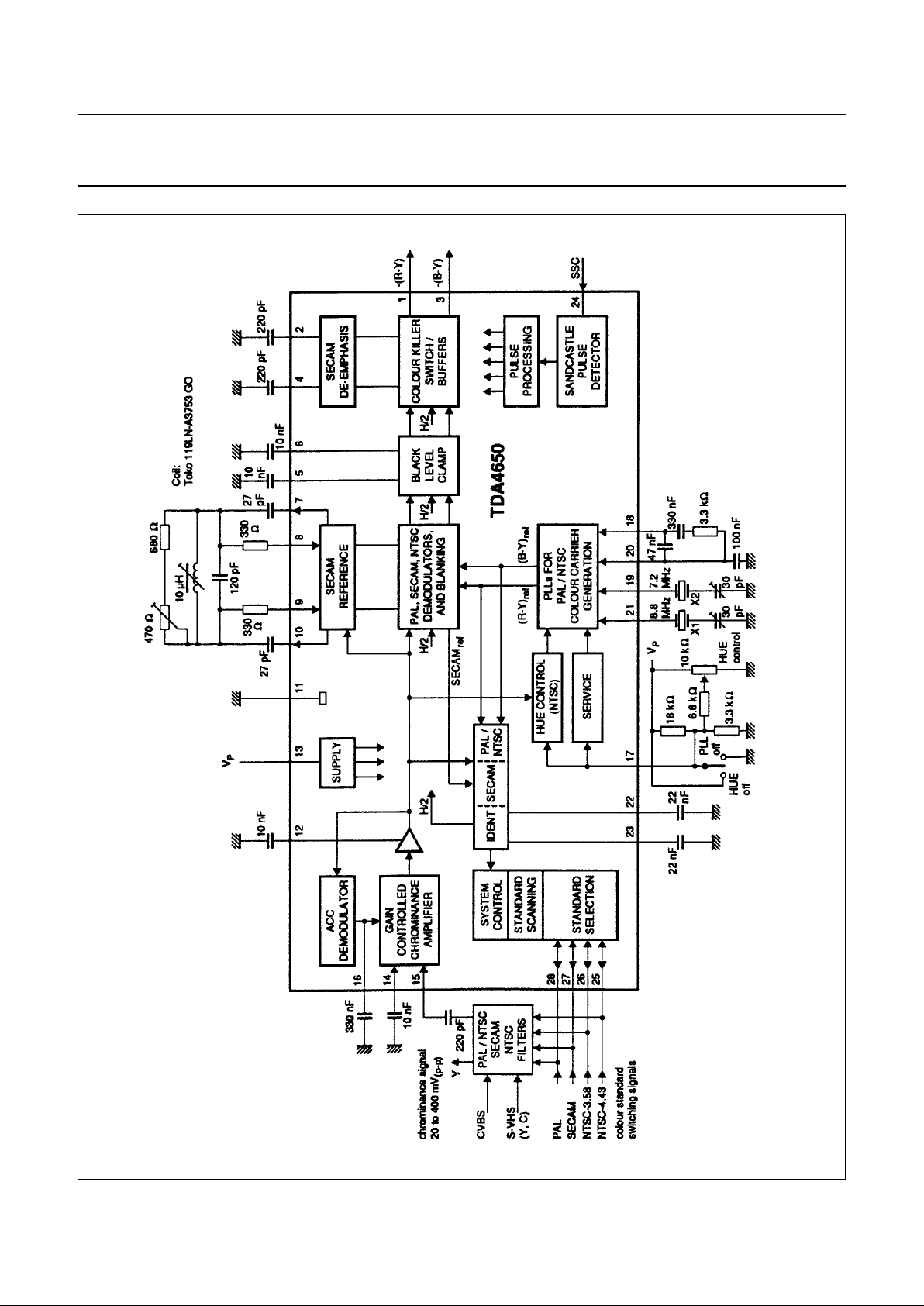
FEATURES
Identifies and demodulates PAL,
SECAM, NTSC 3.58 and NTSC 4.43
chrominance signals with:
• Identification
– automatic standard identification
by sequential inquiry
– secure SECAM identification at
50 Hz only, with PAL priority
– four switched outputs for
chrominance filter selection and
display control
– external service switch for
oscillator adjustment
• PAL / NTSC demodulation
– H (burst) and V blanking
– PAL switch (disabled for NTSC)
– NTSC phase shift (disabled for
PAL)
– PLL-controlled reference
oscillator
– two reference oscillator crystals
on separate pins with automatic
switching
– quadrature demodulator with
subcarrier reference
• SECAM demodulation
– limiter-amplifier
– quadrature-demodulator with a
single external reference tuned
circuit
– alternate line blanking, H and V
blanking
– de-emphasis
• Gain controlled chrominance
amplifier
• ACC demodulation controlled by
system scanning
• Internal colour-difference signal
output filters to remove the residual
subcarrier
GENERAL DESCRIPTION
The TDA4650 is a monolitic
integrated multistandard colour
decoder for PAL, SECAM and NTSC
(3.58 and 4.43 MHz) with negative
colour difference output signals. The
colour-difference output signals are
fed to the TDA4660/TDA4661,
Switched capacitor delay line.
QUICK REFERENCE DATA
ORDERING INFORMATION
Note
1. SOT117-1; 1996 November 28.
2. SOT261-2; 1996 November 28.
SYMBOL PARAMETER CONDITIONS MIN. TYP. MAX. UNIT
V
p
supply voltage range (pin 13) 10.8 12.0 13.2 V
I
p
supply current
(pin 13)
− 60 − mA
v
i(p-p)
chrominance input voltage (pin 15)
(peak-to-peak value)
20 100 400 mV
V
o(p-p)
colour-difference output voltage (pin 1)
(peak-to-peak value)
PAL/NTSC 0.42 0.525 0.66 V
colour-difference output voltage (pin 3)
(peak-to-peak value)
PAL/NTSC 0.53 0.665 0.84 V
colour-difference output voltage (pin 1)
(peak-to-peak value)
SECAM 0.83 1.05 1.32 V
colour-difference output voltage (pin 3)
(peak-to-peak value)
SECAM 1.06 1.33 1.67 V
EXTENDED
TYPE NUMBER
PACKAGE
PINS PIN POSITION MATERIAL CODE
TDA4650 28 DIL plastic SOT117
(1)
TDA4650WP 28 PLCC plastic SOT261
(2)
Page 3
March 1991 3
Philips Semiconductors Preliminary specification
Multistandard colour decoder, with
negative colour difference output signals
TDA4650
Fig.1 Block diagram.
Page 4
March 1991 4
Philips Semiconductors Preliminary specification
Multistandard colour decoder, with
negative colour difference output signals
TDA4650
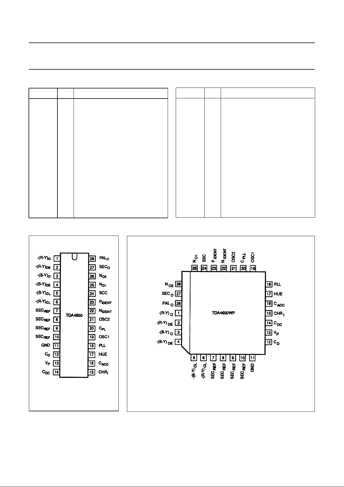
PINNING
SYMBOL PIN DESCRIPTION
−(R-Y)
o
1 −(R-Y) output
−(R-Y)
DE
2 (R-Y) de-emphasis
−(B-Y)
o
3 −(B-Y) output
−(B-Y)
DE
4 (B-Y) de-emphasis
−(B-Y)
CL
5 (B-Y) clamping
−(R-Y)
CL
6 (R-Y) clamping
SEC
REF
7 SECAM reference tuned circuit
SEC
REF
8 SECAM reference tuned circuit
SEC
REF
9 SECAM reference tuned circuit
SEC
REF
10 SECAM reference tuned circuit
GND 11 ground
C
D
12 DC for demodulators
V
P
13 supply voltage
C
DC
14 DC feedback
CHR
I
15 chrominance input
C
ACC
16 automatic colour control
HUE 17 hue control
PLL 18 PLL time constant
OSC1 19 input for 7.15 MHz oscillator
C
PLL
20 PLL DC reference
OSC2 21 input for 8.86 MHz oscillator
N
IDENT
22 NTSC identification
P
IDENT
23 PAL/SECAM identification
SSC 24 super sandcastle pulse input
N
O1
25 NTSC (4.43 MHz) identification
N
O2
26 NTSC (3.58 MHz) identification
SEC
o
27 SECAM identification
PAL
o
28 PAL identification
SYMBOL PIN DESCRIPTION
PIN CONFIGURATIONS
Fig.2 Pin configuration for DIL
package
Fig.3 Pin configuration for PLCC package.
Page 5

March 1991 5
Philips Semiconductors Preliminary specification
Multistandard colour decoder, with
negative colour difference output signals
TDA4650
LIMITING VALUES
In accordance with the Absolute Maximum System (IEC 134)
SYMBOL PARAMETER MIN. MAX. UNIT
V
P
supply voltage (pin 13) − 13.2 V
V
I
voltage range at pins 1, 3, 17 and 24 to 28 0 V
P
V
I
o
output current (pins 1 and 3) −−5mA
I
i/o
input/output current (pins 25 to 28) −−5µA
T
stg
storage temperature range −25 + 150 °C
T
amb
operating ambient temperature range 0 + 70 °C
R
th j-a
from junction to ambient in free air:
SOT117 − 37 K/W
SOT261 − 70 K/W
P
tot
total power dissipation (SOT117) − 1.4 W
total power dissipation (SOT261) − 1.1 W
Fig.4 Internal circuits (continued in Fig.5)
Page 6

March 1991 6
Philips Semiconductors Preliminary specification
Multistandard colour decoder, with
negative colour difference output signals
TDA4650
Fig.5 Internal circuits (continued from Fig.4)
Page 7

March 1991 7
Philips Semiconductors Preliminary specification
Multistandard colour decoder, with
negative colour difference output signals
TDA4650
CHARACTERISTICS
All voltages are measured to GND (pin 1 1); V
P
= 12 V; chrominance input signal V
15(p-p)
= 100 mV (with 75 % colour bar
signal); 4 µs burst-blanking pulse and vertical blanking superimposed on super sandcastle pulse; T
amb
=25°C;
measured in test circuit of Fig.1; unless otherwise specified.
SYMBOL PARAMETER CONDITIONS MIN. TYP. MAX. UNIT
V
P
supply voltage range 10.8 12.0 13.2 V
I
P
supply current 50 60 80 mA
Chrominance part
V
i(p-p)
input signal (pin 15)
(peak-to-peak value)
20 100 400 mV
R
i
input resistance (pin 15) 7 10 13 kΩ
C
i
input capacitance (pin 15) − 45pF
Demodulator part (PAL/NTSC)
V
1(p-p)
colour difference −(R−Y) output
signal (peak-to-peak value)
at nominal phase of hue
control
0.42 0.525 0.66 V
V
3(p-p)
colour difference −(B−Y) output
signal (peak-to-peak value)
at nominal phase of hue
control
0.53 0.665 0.84 V
V
1/V3
ratio of colour difference signals
(R−Y)/(B−Y) for NTSC
at nominal phase of hue
control
0.75 0.79 0.83
V
1/V1
ratio of PAL/NTSC signals
(R−Y)
PAL
/(R−Y)
NTSC
at nominal phase of
hue control
−−1dB
m signal linearity V
1(p-p)
= 0.8 V − (R−Y) 0.8 −−
V
3(p-p)
= 1.0 V − (B−Y) 0.8 −−
V
1,3
DC output level proportional to V
P
6.3 6.8 7.3 V
H/2 ripple at CD outputs without colour bars −−10 mV
V
1,3(p-p)
residual carrier at CD outputs
(peak-to-peak value)
4.43 MHz −−10 mV
8.87 MHz −−30 mV
Z
1,3
output impedance −−200 Ω
Demodulator part (SECAM); note 1
V
1(p-p)
colour difference −(R−Y) output
signal (peak-to-peak value)
every second line blanked 0.83 1.05 1.32 V
V
3(p-p)
colour difference −(B−Y) output
signal (peak-to-peak value)
every second line blanked 1.06 1.33 1.67 V
V
1,3
DC output level proportional to V
P
6.3 6.8 7.3 V
H/2 ripple at CD outputs without colour bars every
second line blanked
−−10 mV
V
1,3(p−p)
residual carrier at CD outputs
(peak-to-peak value)
4.43 MHz −−30 mV
8.87 MHz −−30 mV
Page 8

March 1991 8
Philips Semiconductors Preliminary specification
Multistandard colour decoder, with
negative colour difference output signals
TDA4650
Demodulator part (SECAM) (continued); note 1
∆V
1,3
/∆V
P
shift of blanking levels relative to
demodulated fo levels
−−3 mV/V
∆V
1
/∆T − 0.16 − mV/K
∆V
3
/∆T −−0.25 − mV/K
Hue control part
φ phase shift of reference carrier
relative to phase at V17=3V
V17=2V −30 −40 − deg
phase shift of reference carrier V
17
=3V − 0 ±5 deg
phase shift of reference carrier
relative to phase at V
17
=3V
V17= 4 V 30 40 − deg
V
17
internal bias voltage − 3 − V
switching voltage for oscillator
adjustment
burst OFF; colour ON 0 − 0.5 V
switching voltage for forced
colour ON
burst ON; colour ON 5.5 − V
P
V
R
17
input resistance 3.8 5.0 6.2 kΩ
Reference oscillator (PLL); note 2
R
19,21
input resistance − 350 −Ω
C
19,21
input resistance −−10 pF
f
c
catching range at 4.43 MHz ± 400 −−Hz
at 3.57 MHz ± 330 −−Hz
Identification part
switching voltages for chrominance filters and crystals:
at pin 28 for PAL
at pin 27 for SECAM
at pin 26 for NTSC (3.58 MHz)
at pin 25 for NTSC (4.43 MHz)
V
28 to 25
switching voltages control voltage OFF state − 0.05 0.5 V
control voltage ON state;
during scanning
2.35 2.45 2.55 V
control voltage ON state;
internal forced
5.6 5.8 6.0 V
control voltage ON state;
external forced
9.0 - V
P
V
I
28 to 25
output currents −−−3mA
t
d
delay time for system hold 2 − 3 cycles
delay time for colour ON 2 − 3 cycles
delay time for colour OFF 0 − 1 cycles
t
s
scanning time for each standard note 3 − 4 − cycles
SYMBOL PARAMETER CONDITIONS MIN. TYP. MAX. UNIT
Page 9

March 1991 9
Philips Semiconductors Preliminary specification
Multistandard colour decoder, with
negative colour difference output signals
TDA4650
Notes to the characteristics
1. For the SECAM standard, amplitude and H/2 ripple content of the CD signals (R−Y) and (B−Y) depend on the
characteristics of the external tuned circuit at pins 7 to 10. The resonant frequency of the external tuned circuit must
be adjusted such that the demodulated fo voltage level is zero in the −(B−Y) output channel at pin 3.
Now it is possible to adjust the quality of the external circuit such that the demodulated fo voltage level is zero in the
−(R−Y) output channel at pin 1. If necessary, the fo voltage level in the −(B−Y) output channel must be readjusted to
zero by the coil of the tuned circuit.
The external capacitors at the pins 2 and 4 (220 pF each) are matched to the internal resistances of the de-emphasis
network such that every alternate scanned line is blanked.
2. The fo frequencies of the 8.8 MHz crystal at pin 21, and the 7.2 MHz crystal at pin 19, can be adjusted when the
voltage at pin 17 is less than 0.5 V (burst OFF), thus providing double subcarrier frequencies of the chrominance
signal.
3. The inquiry sequence for the standard is: PAL − SECAM − NTSC (3.58 MHz) −NTSC (4.43 MHz).
PAL has priority with respect to SECAM, etc.
4. The super sandcastle pulse is compared with three internal threshold levels which are proportional to VP.
Super sandcastle pulse detector (note 4)
V
24
input voltage pulse levels to
separate V and H blanking pulses
pulse ON 1.3 1.6 1.9 V
pulse OFF 1.1 1.4 1.7 V
voltage pulse amplitude 2.0 2.5 3.0 V
input voltage pulse levels to
separate H blanking pulse
pulse ON 3.3 3.6 3.9 V
pulse OFF 3.1 3.4 3.7 V
voltage pulse amplitude 4.1 4.5 4.9 V
input voltage pulse levels to
separate burst gating pulse
pulse ON 6.2 6.6 7.0 V
pulse OFF 6.0 6.4 6.8 V
voltage pulse amplitude 7.7 − V
P
V
input voltage during line scan −−1.0 V
I
24
input current during line scan −−−100 µA
SYMBOL PARAMETER CONDITIONS MIN. TYP. MAX. UNIT
Page 10

March 1991 10
Philips Semiconductors Preliminary specification
Multistandard colour decoder, with
negative colour difference output signals
TDA4650
Fig.6 Application diagram with the switched capacitor delay line TDA4660/1.
Page 11

March 1991 11
Philips Semiconductors Preliminary specification
Multistandard colour decoder, with
negative colour difference output signals
TDA4650
PACKAGE OUTLINES
UNIT
A
max.
1 2
b
1
(1)
(1) (1)
cD E weM
H
L
REFERENCES
OUTLINE
VERSION
EUROPEAN
PROJECTION
ISSUE DATE
IEC JEDEC EIAJ
mm
inches
DIMENSIONS (inch dimensions are derived from the original mm dimensions)
SOT117-1
92-11-17
95-01-14
A
min.
A
max.
b
Z
max.
M
E
e
1
1.7
1.3
0.53
0.38
0.32
0.23
36.0
35.0
14.1
13.7
3.9
3.4
0.252.54 15.24
15.80
15.24
17.15
15.90
1.75.1 0.51 4.0
0.066
0.051
0.020
0.014
0.013
0.009
1.41
1.34
0.56
0.54
0.15
0.13
0.010.10 0.60
0.62
0.60
0.68
0.63
0.0670.20 0.020 0.16
051G05 MO-015AH
M
H
c
(e )
1
M
E
A
L
seating plane
A
1
w M
b
1
e
D
A
2
Z
28
1
15
14
b
E
pin 1 index
0 5 10 mm
scale
Note
1. Plastic or metal protrusions of 0.25 mm maximum per side are not included.
handbook, full pagewidth
DIP28: plastic dual in-line package; 28 leads (600 mil)
SOT117-1
Page 12

March 1991 12
Philips Semiconductors Preliminary specification
Multistandard colour decoder, with
negative colour difference output signals
TDA4650
REFERENCES
OUTLINE
VERSION
EUROPEAN
PROJECTION
ISSUE DATE
IEC JEDEC EIAJ
Note
1. Plastic or metal protrusions of 0.01 inches maximum per side are not included.
SOT261-2
19
25
28
1
4
511
18
12
26
detail X
(A )
3
b
p
w M
A
1
A
A
4
L
p
b
1
β
k
1
k
X
y
e
E
B
D
H
E
H
v M
B
D
Z
D
A
Z
E
e
v M
A
0 5 10 mm
scale
92-11-17
95-02-25
pin 1 index
PLCC28: plastic leaded chip carrier; 28 leads
SOT261-2
UNIT A
A
min. max. max. max. max.
1
A
4
b
p
E
(1)
(1) (1)
eH
E
Z
ywv β
mm
4.57
4.19
0.51
3.05
0.53
0.33
0.021
0.013
1.27
0.51
2.16
45
o
0.18 0.100.18
DIMENSIONS (millimetre dimensions are derived from the original inch dimensions)
D
(1)
11.58
11.43
H
D
12.57
12.32
E
Z
2.16
D
b
1
0.81
0.66
k
1.22
1.07
k
1
0.180
0.165
0.020
0.12
A
3
0.25
0.01
0.05
0.020
0.085
0.007 0.0040.007
L
p
1.44
1.02
0.057
0.040
0.456
0.450
11.58
11.43
0.456
0.450
0.495
0.485
12.57
12.32
0.495
0.485
e
E
e
D
10.92
9.91
0.430
0.390
10.92
9.91
0.430
0.390
0.085
0.032
0.026
0.048
0.042
E
e
inches
E
e
Page 13

March 1991 13
Philips Semiconductors Preliminary specification
Multistandard colour decoder, with
negative colour difference output signals
TDA4650
SOLDERING
Introduction
There is no soldering method that is ideal for all IC packages. Wave soldering is often preferred when through-hole and
surface mounted components are mixed on one printed-circuit board. However, wave soldering is not always suitable for
surface mounted ICs, or for printed-circuits with high population densities. In these situations reflow soldering is often
used.
This text gives a very brief insight to a complex technology. A more in-depth account of soldering ICs can be found in our
“IC Package Databook”
(order code 9398 652 90011).
Soldering by dipping or by wave
The maximum permissible temperature of the solder is 260 °C; solder at this temperature must not be in contact with the
joint for more than 5 seconds. The total contact time of successive solder waves must not exceed 5 seconds.
The device may be mounted up to the seating plane, but the temperature of the plastic body must not exceed the
specified maximum storage temperature (T
stg max
). If the printed-circuit board has been pre-heated, forced cooling may
be necessary immediately after soldering to keep the temperature within the permissible limit.
Repairing soldered joints
Apply a low voltage soldering iron (less than 24 V) to the lead(s) of the package, below the seating plane or not more
than 2 mm above it. If the temperature of the soldering iron bit is less than 300 °C it may remain in contact for up to
10 seconds. If the bit temperature is between 300 and 400 °C, contact may be up to 5 seconds.
DEFINITIONS
LIFE SUPPORT APPLICATIONS
These products are not designed for use in life support appliances, devices, or systems where malfunction of these
products can reasonably be expected to result in personal injury. Philips customers using or selling these products for
use in such applications do so at their own risk and agree to fully indemnify Philips for any damages resulting from such
improper use or sale.
Data sheet status
Objective specification This data sheet contains target or goal specifications for product development.
Preliminary specification This data sheet contains preliminary data; supplementary data may be published later.
Product specification This data sheet contains final product specifications.
Limiting values
Limiting values given are in accordance with the Absolute Maximum Rating System (IEC 134). Stress above one or
more of the limiting values may cause permanent damage to the device. These are stress ratings only and operation
of the device at these or at any other conditions above those given in the Characteristics sections of the specification
is not implied. Exposure to limiting values for extended periods may affect device reliability.
Application information
Where application information is given, it is advisory and does not form part of the specification.
 Loading...