

Page 1

INTEGRATED CIRCUITS
DATA SH EET
TDA4557
Multistandard decoder
Product specification
File under Integrated Circuits, IC02
March 1991
Page 2
Philips Semiconductors Product specification
Multistandard decoder TDA4557
GENERAL DESCRIPTION
The TDA4557 is a monolithic integrated multistandard
colour decoder for the PAL, SECAM, NTSC 3.58 MHz and
NTSC 4.43 MHz standards.
FEATURES
Chrominance part
• Gain controlled chrominance amplifier for PAL, SECAM
and NTSC
• ACC rectifier circuits (PAL/NTSC, SECAM)
• Burst blanking (PAL) in front of 64 µs glass delay line
• Chrominance output stage for driving the 64 µs glass
delay line (PAL, SECAM)
• Limiter stages for direct and delayed SECAM signal
• SECAM permutator
Demodulator part
• Flyback blanking incorporated in the demodulators
(PAL, NTSC, SECAM)
• PAL switch
• Internal PAL matrix
• Two quadrature demodulators with external reference
tuned circuits (SECAM)
• Internal filtering of residual carrier
• De-emphasis (SECAM)
Identification part
• Automatic standard recognition by sequential inquiry
• Delay for colour-on and scanning-on
• Reliable SECAM identification by PAL priority circuit and
50/60 Hz recognition
• Forced switch-on of a standard
• Four switching voltages for chrominance filters, traps
and crystals
• Two identification circuits for PAL/SECAM (H/2) and
NTSC
• PAL/SECAM flip-flop
• SECAM identification mode switch (horizontal, vertical
or combined horizontal and vertical)
• Crystal oscillator with divider stages and PLL circuitry
(PAL, NTSC) for double colour subcarrier frequency
• HUE control (NTSC)
• Service switch
QUICK REFERENCE DATA
PARAMETER SYMBOL MIN. TYP. MAX. UNIT
Supply voltage (pin 13) V
Supply current (pin 13) I
Chrominance input voltage
(peak-to-peak value) V
Chrominance output voltage
(peak-to-peak value) V
Colour difference output voltages
(peak-to-peak values)
−(R-Y) V
−(B-Y) V
Sandcastle pulse (pin 24)
Required amplitude to separate
vertical and horizontal pulse V
horizontal pulse V
burst gating pulse V
PACKAGE OUTLINE
P
P
15(p-p)
12(p-p)
1(p-p)
3(p-p)
24(p-p)
24(p-p)
24(p-p)
10.8 12.0 13.2 V
− 65 − mA
20 100 400 mV
− 1.6 − V
− 1.05 V ± 2dB − V
− 1.33 V ± 2dB − V
2.0 2.5 3.0 V
4.1 4.5 4.9 V
7.7 − V
P
V
28-lead DIL; plastic (SOT117); SOT117-1; 1996 November 27.
March 1991 2
Page 3
Philips Semiconductors Product specification
Multistandard decoder TDA4557
March 1991 3
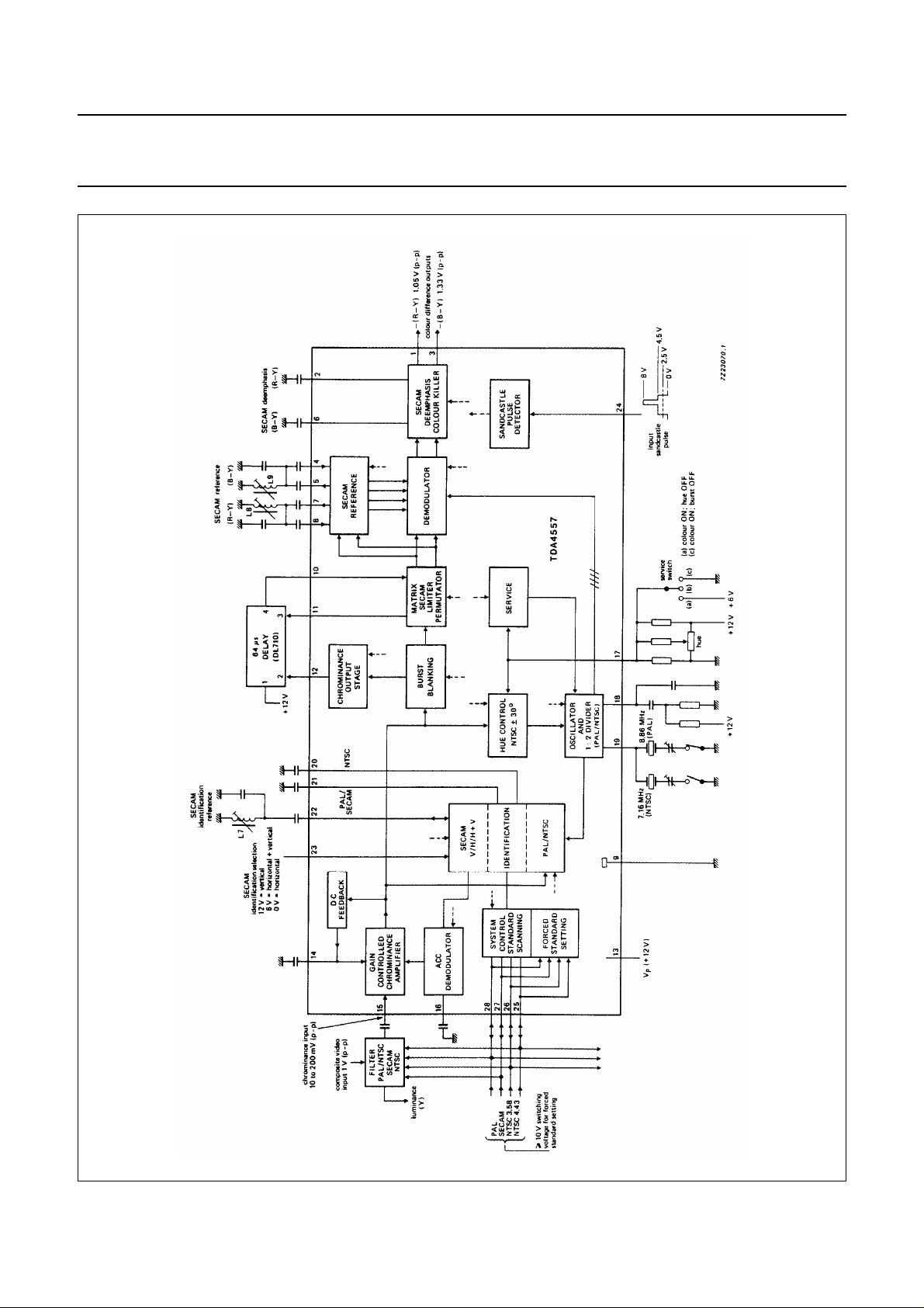
Fig.1 Block diagram.
Page 4

Philips Semiconductors Product specification
Multistandard decoder TDA4557
RATINGS
Limiting values in accordance with the Absolute Maximum System (IEC 134)
PARAMETER SYMBOL MIN. MAX. UNIT
Supply voltage (pin 13) V
Voltage range at pins 10, 11, 17, 23,
24, 25, 26, 27, 28 to pin 9 (ground) V
Current at pin 12 I
Peak value I
Total power dissipation P
Storage temperature range T
Operating ambient temperature range T
P
n-9
12
12M
tot
stg
amb
− 13.2 V
0V
P
V
− 8mA
− 15 mA
− 1.4 W
−25 + 150 °C
0 + 70 °C
March 1991 4
Page 5

Philips Semiconductors Product specification
Multistandard decoder TDA4557
CHARACTERISTICS
V
P=V13-9
= 12 V; T
Supply (pin 13)
Supply voltage range V
Supply current I
Chrominance part
Chrominance input signal (pin 15)
input voltage with 75% colour bar signal
(peak-to-peak value)
input impedance Z
Chrominance output signal (pin 12)
output voltage
(peak-to-peak value)
output impedance
(npn emitter follower)
DC output voltage V
Input for delayed signal (pin 10)
DC input current I
input resistance R
Demodulator part (PAL/NTSC)
Colour difference output signals
output voltage (proportional to V
(peak-to-peak value)
− (R-Y) signal (pin 1) V
−(B-Y) signal (pin 3) V
Ratio of colour difference output signals
(R-Y)/(B-Y) V
Residual carrier (subcarrier frequency)
(peak-to-peak value) V
Residual carrier (PAL only)
(peak-to-peak value) V
H/2 ripple at (R-Y) output (pin 1)
(peak-to-peak value)
without input signal
DC output voltage
npn emitter follower with
internal current source of 0.3 mA
output impedance Z
=25°C; measured in Fig.1; unless otherwise specified
amb
PARAMETER SYMBOL MIN. TYP. MAX. UNIT
10.8 1.2 13.2 V
50 65 80 mA
20 100 400 mV
1.1 1.6 1.75 V
7.3 8.2 9.0 V
−−10 µA
10 −−kΩ
− 1.05 V ± 2dB − V
− 1.33 V ± 2dB − V
− 0.79 ± 10% −
−−30 mV
− 10 − mV
−−10 mV
7.0 7.7 8.4 V
13-9
P
P
V
15(p-p)
710−kΩ
15-9
V
12(p-p)
− −20 Ω
Z
12-9
12-9
10
10-9
)
1(p-p)
3(p-p)
1/3-9
1,3(p-p)
1,3(p-p)
V
1(p-p)
V
1,3-9
− −150 Ω
1,3-9
March 1991 5
Page 6

Philips Semiconductors Product specification
Multistandard decoder TDA4557
PARAMETER SYMBOL MIN. TYP. MAX. UNIT
Demodulator part (SECAM)
Colour difference signals (see note 3)
output voltage (proportional to V
(peak-to-peak value)
−(R-Y) signal (pin 1) V
−(B-Y) signal (pin 3) V
Ratio of colour difference output signals
(R-Y)/(B-Y) V
Residual carrier (4 to 5 MHz)
(peak-to-peak value) V
Residual carrier (8 to 10 MHz)
(peak-to-peak value) V
H/2 ripple
at (R-Y) (B-Y) outputs (pins 1 and 3)
(peak-to-peak value)
with f
signals V
o
DC output voltage V
Shift of inserted levels relative to levels
of demodulated fo frequencies (IC only) ∆V/∆T(R-Y) − 0.5 0.6 mV/K
HUE control (NTSC)/service switch
Phase shift of reference carrier
at V
at V
at V
=2V −φ 30 40 − deg
17-9
=3V φ−0−deg
17-9
=4V +φ 30 40 − deg
17-9
Input resistance R
Service position
Switching voltage (pin 17)
burst OFF; colour ON
(for oscillator adjustment) V
HUE control OFF; colour ON
(for forced colour ON) V
Crystal oscillator (pin 19)
For double colour subcarrier frequency
input resistance R
lock-in-range
referred to subcarrier frequency ∆f ± 400 −−Hz
13-9
)
1(p-p)
3(p-p)
1/3-9
1,3(p-p)
1,3(p-p)
1,3(p-p)
1,3-9
∆V/∆V
17-9
17-9
17-9
19-9
P
− 1.05 − V
− 1.33 − V
− 0.79
(1)
± 10% −
− 20 30 mV
− 20 30 mV
−−30 mV
7.0 7.7 8.4 V
− 8 − mV/V
− 5 − k Ω
0 − 0.5 V
6 − V
V
P
− 350 −Ω
March 1991 6
Page 7

Philips Semiconductors Product specification
Multistandard decoder TDA4557
PARAMETER SYMBOL MIN. TYP. MAX. UNIT
Identification part
Switching voltages for chrominance filters
and crystals
at pin 28 (PAL)
at pin 27 (SECAM)
at pin 26 (NTSC 3.58 MHz)
at pin 25 (NTSC 4.43 MHz)
Control voltage OFF state V
Control voltage ON state
during scanning; colour OFF V
colour ON V
Output current −I
Voltage for forced switching ON
PAL V
SECAM V
NTSC 3.58 MHz V
NTSC 4.43 MHz V
Delay time for
restart of scanning t
colour ON t
colour OFF t
SECAM identification (pin 23)
Input voltage for
horizontal identification (H) V
vertical identification (V) V
combined (H) and (V) identification V
Sequence of standard inquiry
PAL-SECAM-NTSC 3.58 MHz-NTSC
4.43 MHz
Reliable SECAM identification by PAL
priority circuit
Scanning time for each standard t
25,26,27,28-9
25,26,27,28-9
25,26,27,28-9
25,26,27,28-9
28-9
27-9
26-9
25-9
dS
dC1
dC2
23-9
23-9
23-9
S
−−0.5 V
2.1 2.45 2.7 V
5.5 5.8 6.2 V
−−3mA
9 − V
9 − V
9 − V
9 − V
V
P
V
P
V
P
V
P
2 to 3 vertical periods
2 to 3 vertical periods
0 to 1 vertical periods
0 − 2V
10 − V
V
P
− 6 (note 2) − V
4 vertical periods
March 1991 7
Page 8

Philips Semiconductors Product specification
Multistandard decoder TDA4557
PARAMETER SYMBOL MIN. TYP. MAX. UNIT
Sandcastle pulse detector (see note 4)
Input voltage pulse levels (pin 24)
to separate vertical and horizontal
blanking pulses V
required pulse amplitude V
to separate horizontal blanking pulse V
required pulse amplitude V
to separate burst gating pulse V
required pulse amplitude V
Input voltage during horizontal scanning V
Input current −I
24-9
24(p-p)
24-9
24(p-p)
24-9
24(p-p)
24-9
24
Notes
1. Value measured without influence of external circuitry.
2. Or not connected.
3. The signal amplitude of the colour difference signals (R-Y) and (B-Y) is dependent on the characteristics of the
external tuned circuits at pins 7, 8 and 4, 5 respectively. Adjustment of the amplitude is achieved by varying the
Q-factor of these tuned circuits. The resonant frequency must be adjusted such that the demodulated output
frequency (fo) provides the same output level as the internally inserted reference voltage (achromatic value).
4. The sandcastle pulse is compared with three internal threshold levels, which are proportional to the supply voltage.
1.3 1.6 1.9 V
2.0 2.5 3.0 V
3.3 3.6 3.9 V
4.1 4.5 4.9 V
6.6 7.1 7.6 V
7.7 − V
V
P
−−1.0 V
−−100 µA
March 1991 8
Page 9

Philips Semiconductors Product specification
Multistandard decoder TDA4557
APPLICATION INFORMATION
March 1991 9
Service switch
(a) colour ON; hue OFF
(c) colour ON; burst OFF
Fig.2 Application diagram.
Page 10

Philips Semiconductors Product specification
Multistandard decoder TDA4557
PACKAGE OUTLINE
handbook, full pagewidth
DIP28: plastic dual in-line package; 28 leads (600 mil)
SOT117-1
seating plane
L
Z
28
1
pin 1 index
D
A
2
A
A
1
e
b
w M
b
1
15
E
14
c
M
(e )
M
E
1
H
0 5 10 mm
scale
DIMENSIONS (inch dimensions are derived from the original mm dimensions)
A
A
A
UNIT
inches
Note
1. Plastic or metal protrusions of 0.25 mm maximum per side are not included.
max.
mm
OUTLINE
VERSION
SOT117-1
1 2
min.
max.
1.7
1.3
0.066
0.051
IEC JEDEC EIAJ
051G05 MO-015AH
b
b
1
0.53
0.38
0.020
0.014
0.32
0.23
0.013
0.009
REFERENCES
cD E weM
(1) (1)
36.0
35.0
1.41
1.34
March 1991 10
14.1
13.7
0.56
0.54
(1)
92-11-17
95-01-14
Z
max.
1.75.1 0.51 4.0
0.0670.20 0.020 0.16
L
3.9
15.80
3.4
15.24
EUROPEAN
PROJECTION
M
0.62
0.60
H
E
17.15
15.90
0.68
0.63
0.252.54 15.24
0.010.10 0.60
ISSUE DATE
e
1
0.15
0.13
Page 11

Philips Semiconductors Product specification
Multistandard decoder TDA4557
SOLDERING
Introduction
There is no soldering method that is ideal for all IC
packages. Wave soldering is often preferred when
through-hole and surface mounted components are mixed
on one printed-circuit board. However, wave soldering is
not always suitable for surface mounted ICs, or for
printed-circuits with high population densities. In these
situations reflow soldering is often used.
This text gives a very brief insight to a complex technology.
A more in-depth account of soldering ICs can be found in
“IC Package Databook”
our
Soldering by dipping or by wave
The maximum permissible temperature of the solder is
260 °C; solder at this temperature must not be in contact
with the joint for more than 5 seconds. The total contact
time of successive solder waves must not exceed
5 seconds.
DEFINITIONS
Data sheet status
Objective specification This data sheet contains target or goal specifications for product development.
Preliminary specification This data sheet contains preliminary data; supplementary data may be published later.
Product specification This data sheet contains final product specifications.
(order code 9398 652 90011).
The device may be mounted up to the seating plane, but
the temperature of the plastic body must not exceed the
specified maximum storage temperature (T
printed-circuit board has been pre-heated, forced cooling
may be necessary immediately after soldering to keep the
temperature within the permissible limit.
Repairing soldered joints
Apply a low voltage soldering iron (less than 24 V) to the
lead(s) of the package, below the seating plane or not
more than 2 mm above it. If the temperature of the
soldering iron bit is less than 300 °C it may remain in
contact for up to 10 seconds. If the bit temperature is
between 300 and 400 °C, contact may be up to 5 seconds.
stg max
). If the
Limiting values
Limiting values given are in accordance with the Absolute Maximum Rating System (IEC 134). Stress above one or
more of the limiting values may cause permanent damage to the device. These are stress ratings only and operation
of the device at these or at any other conditions above those given in the Characteristics sections of the specification
is not implied. Exposure to limiting values for extended periods may affect device reliability.
Application information
Where application information is given, it is advisory and does not form part of the specification.
LIFE SUPPORT APPLICATIONS
These products are not designed for use in life support appliances, devices, or systems where malfunction of these
products can reasonably be expected to result in personal injury. Philips customers using or selling these products for
use in such applications do so at their own risk and agree to fully indemnify Philips for any damages resulting from such
improper use or sale.
March 1991 11
 Loading...