

Page 1

INTEGRATED CIRCUITS
DATA SH EET
TDA3608Q; TDA3608TH
Multiple voltage regulators with
switch
Product specification
Supersedes data of 2000 Oct 13
File under Integrated Circuits, IC01
2001 Jun 29
Page 2

Philips Semiconductors Product specification
Multiple voltage regulators with switch TDA3608Q; TDA3608TH
FEATURES
General
• Two VP-state controlled regulators (regulator 1 and
regulator 3) and a power switch
• Regulator 2 and reset circuit operate during load dump
and thermal shutdown
• Separate control pins for switching regulator 1,
regulator 3 and power switch
• Supply voltage range from −18 to +50 V
• Low reverse current of regulator 2
• Low quiescent current (when regulator 1, regulator 3
and power switch are switched off)
• Hold output circuit for regulator 1 (only valid when
regulator 3 output voltage >1.3 V)
• Reset and hold outputs (open-collector outputs)
• Adjustable reset delay time
• High ripple rejection
• Backup capacitor connection to supply regulator 2 and
reset circuit up to 25 V.
Protections
• Reverse polarity safe (down to −18 V without high
reverse current)
• Able to withstand voltages up to 18 V at the outputs
(supply line may be short circuited)
• ESD protection on all pins
• Thermal protection
• Load dump protection
• Foldback current limit protection for regulator 1,
regulator 2 and regulator 3
• Delayed foldback current limit protection for power
switch (at short-circuit); delay time fixed by reset delay
capacitor
• All regulator outputs and power switch are
DC short-circuited safe to ground and VP.
GENERAL DESCRIPTION
The TDA3608 isamultiple output voltage regulator with a
power switch, intended for use in car radios with or without
a microcontroller. It contains:
• Two fixed output voltage regulators with a foldback
current protection (regulator 1 and regulator 3) and one
fixed output voltage regulator (regulator 2) intended to
supply a microcontroller, which also operates during
load dump and thermal shutdown
• A power switch with protections, operated by an enable
input
• Reset and hold outputs that can be used to interface
with the microcontroller; the reset output can be used to
call up the microcontroller and the hold output indicates
thattheregulator 1 output voltage is available and within
the range
• A supply pin which can withstand load dump pulses and
negative supply voltages
• Regulator 2 which is switched on at a backup voltage
higher than 6.5 V and switched off when the regulator 2
output drops below 1.9 V
• A provision for the use of a reserve (backup) supply
capacitor that will hold enough energy for regulator 2
(5 Vcontinuous) to allow a microcontrollertoprepare for
loss of voltage.
ORDERING INFORMATION
TYPE
NUMBER
TDA3608Q DBS13P plastic DIL-bent-SIL power package; 13 leads (lead length 12 mm) SOT141-6
TDA3608TH HSOP20 plastic, heatsink small outline package; 20 leads; low stand-off height SOT418-2
2001 Jun 29 2
NAME DESCRIPTION VERSION
PACKAGE
Page 3
Philips Semiconductors Product specification
Multiple voltage regulators with switch TDA3608Q; TDA3608TH
QUICK REFERENCE DATA
SYMBOL PARAMETER CONDITIONS MIN. TYP. MAX. UNIT
Supply
V
P
I
q
T
j
Voltage regulators
V
REG1
V
REG2
V
REG3
Power switch
V
drop
I
M
supply voltage operating 9.5 14.4 18 V
regulator 2 on 2.4 14.4 18 V
reverse polarity; non-operating −−−18 V
jump start for t ≤ 10 minutes −−30 V
load dump protection for t ≤ 50 ms
and t
≥ 2.5 ms
r
−−50 V
quiescent supply current standby mode; VP= 12.4 V − 500 600 µA
junction temperature −40 − +150 °C
output voltage of regulator 1 1 mA ≤ I
output voltage of regulator 2 0.5 mA ≤ I
output voltage of regulator 3 1 mA ≤ I
≤ 600 mA 8.15 8.5 8.85 V
REG1
≤ 150 mA 4.75 5.0 5.25 V
REG2
≤ 400 mA 4.75 5.0 5.25 V
REG3
dropout voltage ISW=1A − 0.45 0.7 V
I
= 1.8 A − 1.0 1.8 V
SW
peak current 2 −−A
2001 Jun 29 3
Page 4
Philips Semiconductors Product specification
Multiple voltage regulators with switch TDA3608Q; TDA3608TH
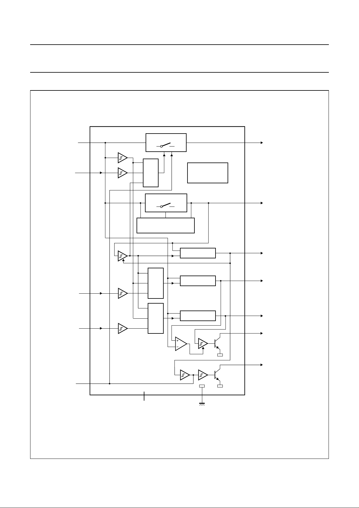
BLOCK DIAGRAM
handbook, full pagewidth
(14.4 V)
V
1 (3)
P
POWER SWITCH
(17) 13
SW
(14.2 V/1.8 A)
ENSW
EN3
EN1
7 (10)
4 (6)
6 (9)
&
BACKUP SWITCH
BACKUP CONTROL
&
&
TEMPERATURE
AND LOAD DUMP
PROTECTION
REGULATOR 2
REGULATOR 3
REGULATOR 1
(16) 12
(15) 11
(5) 3
(4) 2
(11) 8
BU
REG2
REG3
REG1
HOLD
(14.2 V/100 mA)
(5 V/150 mA)
(5 V/400 mA)
(8.5 V/600 mA)
TDA3608Q
hold enable
(TDA3608TH)
C
9 (12)
RES
(1, 2, 7, 13, 18, 19, 20)
n.c.
Numbers in parenthesis refer to type number TDA3608TH.
Fig.1 Block diagram.
2001 Jun 29 4
10 (14)
GND
(8) 5
MGK602
RES
Page 5
Philips Semiconductors Product specification
Multiple voltage regulators with switch TDA3608Q; TDA3608TH
PINNING
SYMBOL
DESCRIPTION
TDA3608Q TDA3608TH
PIN
V
P
1 3 supply voltage
REG1 2 4 regulator 1 output
REG3 3 5 regulator 3 output
EN3 4 6 regulator 3 enable input
RES 5 8 reset output
EN1 6 9 regulator 1 enable input
ENSW 7 10 power switch enable input
HOLD 8 11 hold output
C
RES
9 12 reset delay capacitor connection
GND 10 14 ground
REG2 11 15 regulator 2 output
BU 12 16 backup capacitor connection
SW 13 17 power switch output
n.c. − 1, 2, 7, 13, 18,
not connected
19 and 20
handbook, halfpage
Fig.2 Pin configuration of TDA3608Q.
V
REG1
REG3
EN3
RES
EN1
ENSW
HOLD
C
RES
GND
REG2
BU
SW
P
1
2
3
4
5
6
TDA3608Q
7
8
9
10
11
12
13
MGK601
handbook, halfpage
Fig.3 Pin configuration of TDA3608TH.
n.c.
n.c.
n.c.
SW
BU
REG2
GND
n.c.
C
RES
HOLD
20
19
18
17
16
TDA3608TH
15
14
13
12
11
MGT566
10
1
2
3
4
5
6
7
8
9
n.c.
n.c.
V
P
REG1
REG3
EN3
n.c.
RES
EN1
ENSW
2001 Jun 29 5
Page 6

Philips Semiconductors Product specification
Multiple voltage regulators with switch TDA3608Q; TDA3608TH
FUNCTIONAL DESCRIPTION
The TDA3608 is a multiple output voltage regulator with a
power switch, intended for use in car radios with or without
a microcontroller. Because of low-voltage operation of the
car radio, low-voltage drop regulators are used in the
TDA3608.
Backup supply
The charge of the backup capacitor connected to pin BU
can be used to supply regulator 2 for a short period when
the supply voltage VP drops to 0 V (the time depends on
the value of the capacitor).
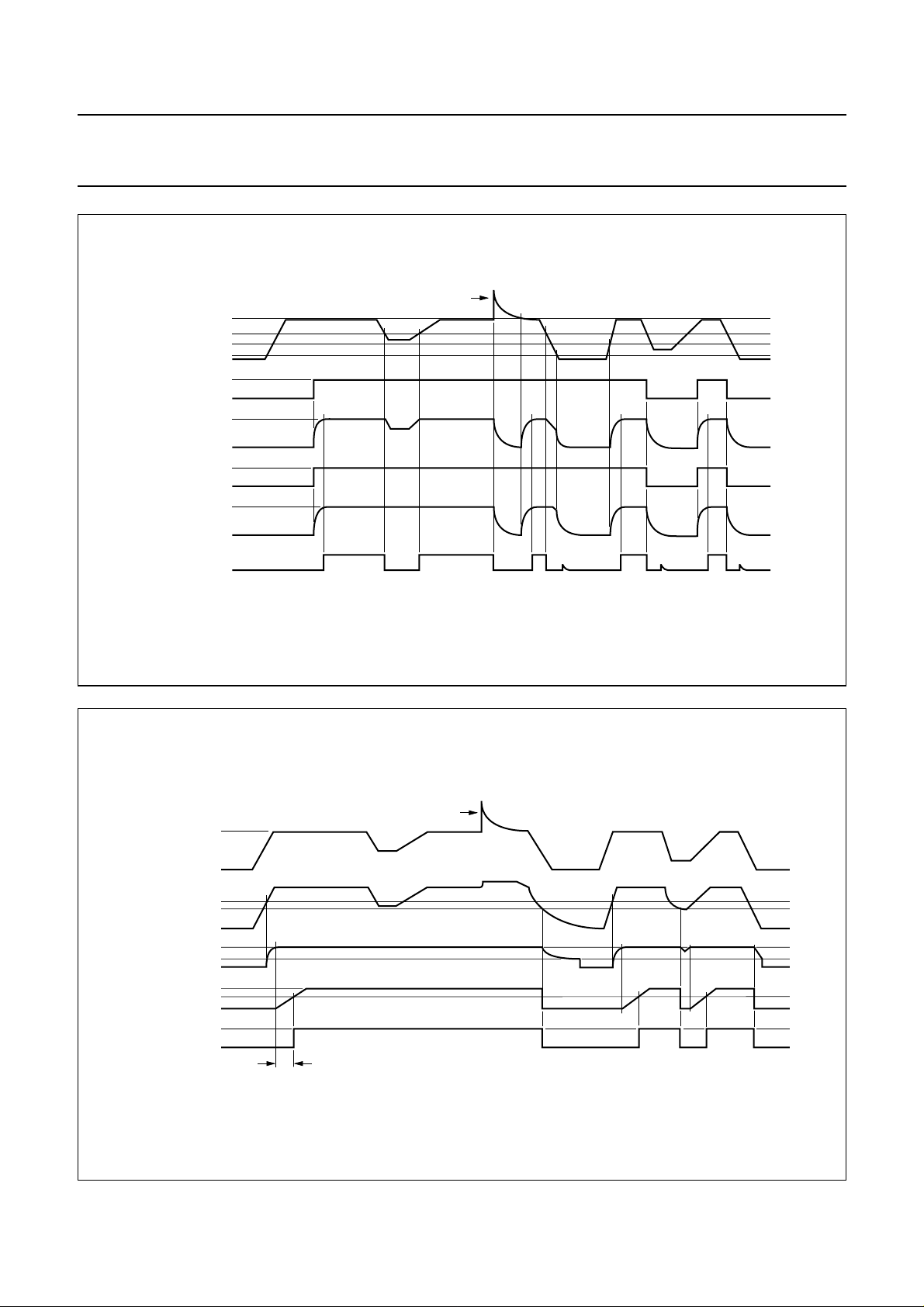
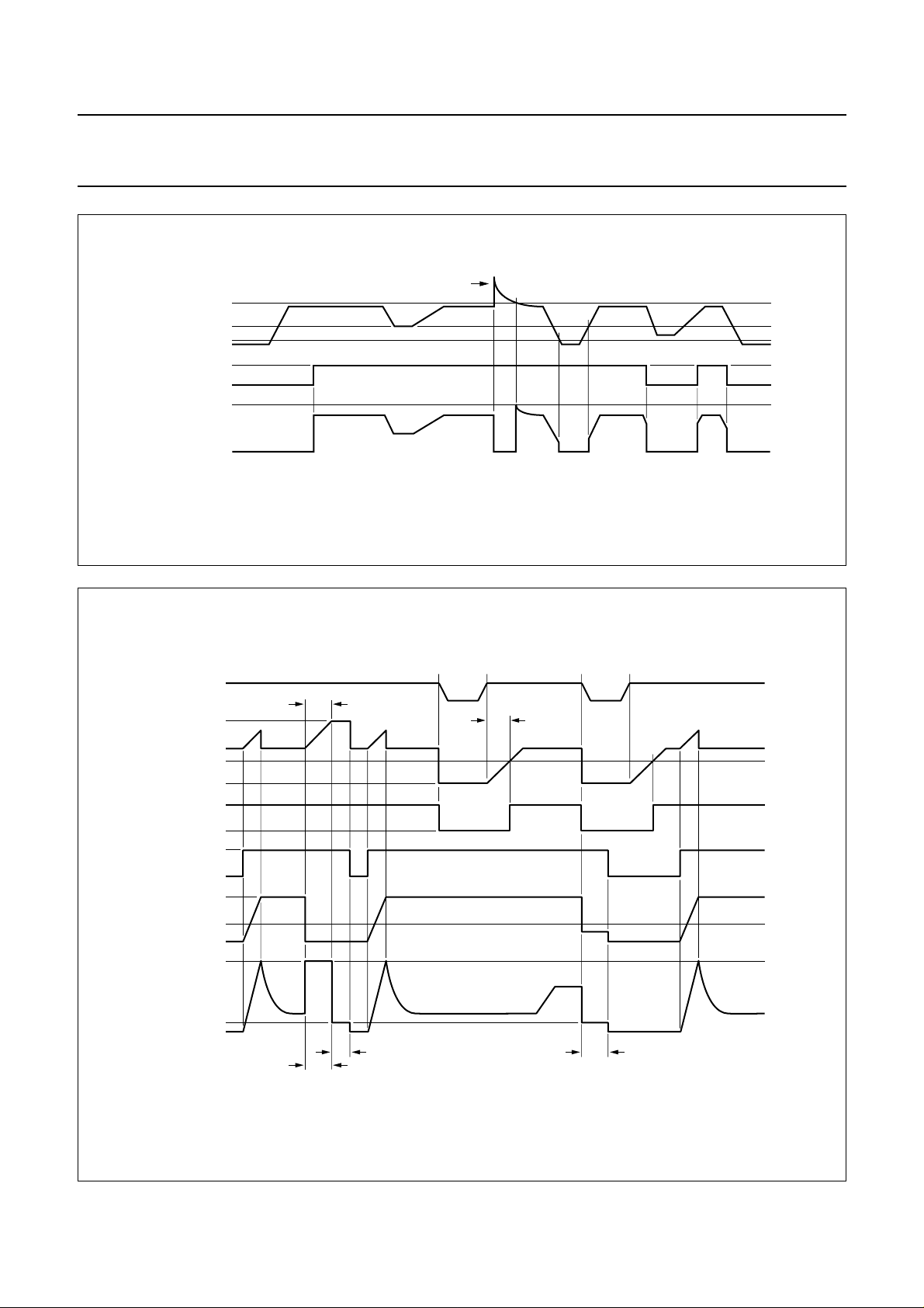
Regulator 1
When the output voltage of regulator 2 and the supply
voltage (VP> 4.5 V) are both available, regulator 1 can be
operated by means of enable pin EN1 (see Fig.4).
Regulator 2
Regulator 2 switches on (see Fig.5) when the backup
voltage exceeds 6.5 V for the first time and switches off
when the output voltage of regulator 2 drops below 1.9 V
(this is far below an engine start).
The hold output is only activated when V
REG3
> 1.3 V.
When pin HOLD is connected via a pull-up resistor to the
output of regulator 3 spikes will be minimized to 1.3 V
(maximum value) because the hold output is only disabled
when V
REG3
< 1.3 V.
Pin HOLD will be forced LOW when the load dump
protection is activated and also in the standby mode.
Power switch
The power switch can be controlled by means of enable
pin ENSW (see Fig.6).
Protections
All output pins are fully protected.
The regulators are protected against load dump
(regulator 1 and regulator 3 switch off at VP> 18 V) and
short-circuit (foldback current protection).
The power switch contains a foldback current protection,
but this protection is delayed at a short-circuit condition by
the reset delay capacitor. During this time the output
current is limited to at least 2 A (peak value) and
1.8 A (continuous value) at VP≤ 18 V. During the foldback
mode the current is limited to 0.5 A (typical value).
Regulator 3
When the output voltage of regulator 2 and the supply
voltage (VP> 4.5 V) are both available, regulator 3 can be
operated by means of enable pin EN3 (see Fig.4).
Reset
When regulator 2 is switched on and the output voltage of
this regulator is within its voltage range, the reset output
(see Fig.5) will be enabled (pin RES goes HIGH through
an external pull-up resistor) to generate a reset to the
microcontroller.
The reset cycles can be extended by means of anexternal
capacitor connected to pin C
. This start-up feature is
RES
included to secure asmooth start-up ofthe microcontroller
at first connection, without uncontrolled switching of
regulator 2 during the start-up sequence.
Hold
Regulator 1 has an open-collector hold output (see Fig.4)
indicating that the output voltage is settled at 8.5 V.
Pin HOLD is held HIGH by an external pull-up resistor.
When the supply voltage VPdrops or during high load, the
output voltage drops out-of-regulationand pin HOLD goes
LOW.
The timing diagram is shown in Fig.7.
The foldback protection is activated when VSW<4V.
When regulator 2 is out-of-regulation and generates a
reset, the power switch is in the foldback mode
immediately when VSW<4V.
In the standby mode the voltage on the reset delay
capacitor is about 4 V and the voltage on the power switch
output is VP− 0.45 V (typical value) at ISW= 1 A. During
an overload condition or short-circuit the reset delay
capacitor will be charged to a higher voltage. The power
switch is in the high current mode while the capacitor is
charged, after this the switch is in the foldback mode
(VSW< 4 V).Whilethe reset delay capacitor is charged the
power switch output can reach its correct output voltage.
Now the voltage on the reset delay capacitor is decreased
rapidlyto 4 V. The resetoutput voltage is not influencedby
this change of voltages. The time of the high current mode
depends on the value of the reset delay capacitor.
At VP> 18 V the power switch is clamped at maximum
17.2 V (to avoid that external connected circuitry is being
damaged by an overvoltage) and the power switch will
switch off at load dump.
2001 Jun 29 6
Page 7
Philips Semiconductors Product specification
Multiple voltage regulators with switch TDA3608Q; TDA3608TH
handbook, full pagewidth
V
P
enable
regulator 1
regulator 1
enable
regulator 3
regulator 3
hold output
18.0 V
9.5 V
4.5 V
4.0 V
≥2.2 V
≤2.0 V
8.5 V
0 V
≥2.2 V
≤2.0 V
5.0 V
0 V
load dump
MGT568
Fig.4 Timing diagram of regulator 1, regulator 3 and hold output.
handbook, full pagewidth
V
P
backup
regulator 2
reset
delay
capacitor
reset
output
18.0 V
4.0 V
6.5 V
5.4 V
5.0 V
1.9 V
0 V
5.0 V
3.0 V
0 V
5.0 V
t
d(res)
load dump
Fig.5 Timing diagram of backup, regulator 2 and reset output.
2001 Jun 29 7
MGT567
Page 8
Philips Semiconductors Product specification
Multiple voltage regulators with switch TDA3608Q; TDA3608TH
handbook, full pagewidth
V
P
enable
power
switch
power
switch
output
handbook, full pagewidth
regulator 2
reset
delay
voltage
reset
output
enable
power
switch
power
switch
voltage
power
switch
current
18.0 V
4.5 V
4.0 V
≥2.2 V
≤2.0 V
16.2 V
0 V
5 V
6.4 V
4 V
3 V
0 V
5 V
0 V
>
2.2 V
<
2.0 V
14 V
4 V
0 V
2 A
0.5 A
0 A
current limit mode
load dump
Fig.6 Timing diagram of power switch output.
t
d(sw)
foldback mode foldback mode
t
d(res)
MGT569
MGT570
Fig.7 Timing diagram of current protection of power switch.
2001 Jun 29 8
Page 9

Philips Semiconductors Product specification
Multiple voltage regulators with switch TDA3608Q; TDA3608TH
LIMITING VALUES
In accordance with the Absolute Maximum Rating System (IEC 60134).
SYMBOL PARAMETER CONDITIONS MIN. MAX. UNIT
V
P
P
tot
T
stg
T
amb
T
j
THERMAL CHARACTERISTICS
supply voltage operating − 18 V
reverse polarity; non-operating −−18 V
jump start for t ≤ 10 minutes − 30 V
load dump protection for t ≤ 50 ms and
t
≥ 2.5 ms
r
− 50 V
total power dissipation − 62 W
storage temperature non-operating −55 +150 °C
ambient temperature operating −40 +85 °C
junction temperature operating −40 +150 °C
SYMBOL PARAMETER CONDITIONS VALUE UNIT
R
th(j-c)
thermal resistance from junction to case
TDA3608Q 2 K/W
TDA3608TH 3.5 K/W
R
th(j-a)
thermal resistance from junction to ambient in free air 50 K/W
CHARACTERISTICS
V
= 14.4 V; T
P
=25°C; measured in test circuit of Fig.12; unless otherwise specified.
amb
SYMBOL PARAMETER CONDITIONS MIN. TYP. MAX. UNIT
Supply
V
P
supply voltage operating 9.5 14.4 18 V
regulator 2 on; note 1 2.4 14.4 18 V
jump start for t ≤ 10 minutes −− 30 V
load dump protection for
t ≤ 50 ms and t
I
q
quiescent supply
current
standby mode; note 2
= 12.4 V − 500 600 µA
V
P
V
= 14.4 V − 520 −µA
P
≥ 2.5 ms
r
−− 50 V
Schmitt trigger supply voltage for regulator 1, regulator 3 and power switch
V
thr
V
thf
V
hys
rising threshold voltage 4.0 4.5 5.0 V
falling threshold voltage 3.5 4.0 4.5 V
hysteresis voltage − 0.5 − V
Schmitt trigger supply voltage for regulator 2
V
thr
V
thf
V
hys
rising threshold voltage 6.0 6.5 7.1 V
falling threshold voltage 1.7 1.9 2.2 V
hysteresis voltage − 4.6 − V
2001 Jun 29 9
Page 10

Philips Semiconductors Product specification
Multiple voltage regulators with switch TDA3608Q; TDA3608TH
SYMBOL PARAMETER CONDITIONS MIN. TYP. MAX. UNIT
Schmitt trigger voltage for enable input (regulator 1, regulator 3 and power switch)
V
thr
V
thf
V
hys
I
LI
Schmitt trigger voltage for reset
V
thr
V
thf
V
hys
Schmitt trigger voltage for hold
V
thr
V
thf
V
hys
Reset and hold output
I
sinkL
I
LO
t
r
t
f
Reset delay capacitor circuit
I
ch
I
dch
V
thr(res)
V
thr(sw)
t
d(res)
Regulator 1; I
V
REG1(off)
V
REG1
∆V
line
∆V
load
I
q
SVRR supply voltage ripple
rising threshold voltage 1.7 2.2 2.7 V
falling threshold voltage 1.5 2.0 2.5 V
hysteresis voltage I
REG=ISW
= 1 mA 0.1 0.2 0.5 V
input leakage current VEN=5V 1 5 10 µA
rising threshold voltage
VPrising; I
= 50 mA; note 3 − V
REG2
REG2
− 0.15 V
REG2
− 0.075 V
of regulator 2
fallingthresholdvoltage
VPfalling; I
= 50 mA; note 3 4.3 V
REG2
− 0.35 − V
REG2
of regulator 2
hysteresis voltage 0.1 0.2 0.3 V
rising threshold voltage
VPrising; note 3 − V
REG1
− 0.15 V
REG1
− 0.075 V
of regulator 1
fallingthresholdvoltage
VPfalling; note 3 7.7 V
− 0.35 − V
REG1
of regulator 1
hysteresis voltage 0.1 0.2 0.3 V
LOW-level sink current Vo≤ 0.8 V 2 −− mA
output leakage current Vo=5V; VP= 14.4 V −− 2 µA
rise time note 4 − 750µs
fall time note4 − 150µs
charge current 2 3 4 µA
discharge current 500 800 −µA
rising threshold voltage
2.8 3.0 3.2 V
for delayed reset pulse
rising threshold voltage
note 5 − 6.4 − V
for delayed power
switch foldback mode
reset delay time C7 = 47 nF; note 6 32 47 70 ms
= 5 mA; unless otherwise specified
REG1
output voltage with
− 1 400 mV
regulator off
output voltage 1 mA ≤ I
9.5 V ≤ V
≤ 600 mA 8.15 8.5 8.85 V
REG1
≤ 18 V 8.15 8.5 8.85 V
P
line regulation 9.5 V ≤ VP≤ 18 V − 275mV
load regulation 1 mA ≤ I
quiescent current I
= 600 mA − 25 60 mA
REG1
= 3 kHz; Vi= 2 V (p-p) 60 70 − dB
f
i
≤ 600 mA − 20 50 mV
REG1
rejection
2001 Jun 29 10
Page 11

Philips Semiconductors Product specification
Multiple voltage regulators with switch TDA3608Q; TDA3608TH
SYMBOL PARAMETER CONDITIONS MIN. TYP. MAX. UNIT
V
drop
I
m
I
sc
Regulator 2; I
V
REG2
∆V
line
∆V
load
SVRR supply voltage ripple
V
drop
I
m
I
sc
Regulator 3; I
V
REG3(off)
V
REG3
∆V
line
∆V
load
I
q
SVRR supply voltage ripple
V
drop
I
m
I
sc
dropout voltage VP= 8.5 V; I
REG1
= 550 mA;
− 0.4 0.7 V
note 7
current limit V
> 7.5 V; see Fig.8; note 8 0.65 1.2 − A
REG1
short-circuit current RL≤ 0.5 Ω; see Fig.8; note 9 250 800 − mA
= 5 mA; unless otherwise specified
REG2
output voltage 0.5 mA ≤ I
= 300 mA; note 10 4.75 5.0 5.25 V
I
REG2
7V≤V
P
18 V ≤ V
I
≤ 150 mA
REG2
≤ 150 mA 4.75 5.0 5.25 V
REG2
≤18 V 4.75 5.0 5.25 V
≤ 50 V;
P
4.75 5.0 5.25 V
line regulation 6 V ≤ VP≤ 18 V − 250mV
18 V ≤ V
load regulation 1 mA ≤ I
1mA≤I
f
= 3 kHz; Vi= 2 V (p-p) 60 70 − dB
i
≤ 50 V − 15 75 mV
P
≤ 150 mA − 20 50 mV
REG2
≤ 300 mA −− 100 mV
REG2
rejection
dropout voltage normal supply; note 7
V
= 4.75 V; I
P
V
= 5.75 V; I
P
= 100 mA − 0.4 0.6 V
REG2
= 200 mA − 0.8 1.2 V
REG2
backup supply; note 11
V
current limit V
= 4.75 V; I
BU
V
= 5.75 V; I
BU
> 4.5 V; see Fig.9; note 8 0.32 0.37 − A
REG2
= 100 mA − 0.2 0.5 V
REG2
= 200 mA − 0.8 1.0 V
REG2
short-circuit current RL≤ 0.5 Ω; see Fig.9; note 9 20 100 − mA
= 5 mA; unless otherwise specified
REG3
output voltage with
− 1 400 mV
regulator off
output voltage 1 mA ≤ I
7V≤V
≤ 400 mA 4.75 5.0 5.25 V
REG3
≤18 V 4.75 5.0 5.25 V
P
line regulation 7 V ≤ VP≤ 18 V − 250mV
load regulation 1 mA ≤ I
quiescent current I
= 400 mA − 15 40 mA
REG3
f
= 3 kHz; Vi= 2 V (p-p) 60 70 − dB
i
≤ 400 mA − 20 50 mV
REG3
rejection
dropout voltage VP= 5.75 V; I
REG3
= 400 mA;
− 1 1.5 V
note 7
current limit V
> 4.5 V; see Fig.10;
REG3
0.45 0.70 − A
note 8
short-circuit current RL≤ 0.5 Ω; see Fig.10; note 9 100 400 − mA
2001 Jun 29 11
Page 12

Philips Semiconductors Product specification
Multiple voltage regulators with switch TDA3608Q; TDA3608TH
SYMBOL PARAMETER CONDITIONS MIN. TYP. MAX. UNIT
Power switch
V
drop
V
cl
V
fb
I
dc
I
M
I
sc
Backup switch
I
dc
V
cl
I
r
Notes
1. The minimum value is the minimum operating voltage, only if VP has exceeded 6.5 V.
2. The quiescent current is measured in the standby mode. Therefore, the enable inputs of regulator 1, regulator 3 and
the power switch are grounded and R
3. The voltage of the regulator drops as a result of a VPdrop.
4. The rise and fall time is measured with a 10 kΩ pull-up resistor and CL=50pF.
5. Thisis the threshold voltage for thedelaytimeof the power switch. The voltageonthe reset delay capacitor increases
only at low output voltage of the power switch (for example at short circuit). When the voltage on this capacitor
exceeds this threshold voltage, the power switch is set to the foldback mode. The power switch is also protected by
the temperature protection.
6. Delay time calculation:
dropout voltage ISW= 1 A; note 12 − 0.45 0.7 V
I
= 1.8 A; note 12 − 1.0 1.8 V
SW
clamping voltage VP≥ 18 V 15 16.2 17.2 V
flyback voltage
ISW= −100 mA − VP+ 3 22 V
behaviour
continuous current VP=16V; VSW= 13.5 V 1.8 2.0 − A
peak current VP= 17 V; see Fig.11; note 13 2 −− A
short-circuit current VP= 14.4 V; VSW< 3.5 V;
− 0.5 − A
see Fig.11; note 14
continuous current 0.3 0.35 − A
clamping voltage VP≥ 16.7 V −− 16 V
reverse current VP= 0; VBU= 12.4 V; note 15 −− 900 mA
L(REG2)
= ∞.
d(sw)
C
V
× C 1000 103××== sec[]
------
C (th1)
I
ch
C
× C 500× 103×== sec[]
V
------
C (th2)
I
ch
and pins REG1, REG2
P
a) Reset pulse delay: The delay time is 47 ms for C = 47 nF.
b) Power switch delay: The delay time is 23.5 ms for C = 47 nF.
t
d(res)
t
7. The dropout voltage of regulator 1, regulator 2 and regulator 3 is measured between pin V
or REG3 respectively.
8. During current limit, current Im is held constant.
9. The foldback current protection limits the dissipated power at short-circuit.
10. The peak current of 300 mA can only be applied for short periods (t < 100 ms).
11. The dropout voltage is measured between pins BU and REG2.
12. The dropout voltage of the power switch is measured between pins VP and SW.
13. The maximum output current of the power switch is limited to 1.8 A when VP>18V.
2001 Jun 29 12
Page 13

Philips Semiconductors Product specification
Multiple voltage regulators with switch TDA3608Q; TDA3608TH
14. During short-circuit, current Iscof the power switch is held constant to a lower value than the continuous current after
a delay of at least 10 ms. Furthermore, a foldback function is activated after the delay. When VSW< 3.5 V, the
short-circuit current is reduced to 0.5 A (typical value). The short-circuit protection of the power switch functions best
when C1 = 220 µF and C2 = 10 µF.
15. The reverse current of the backup switch is the current which is flowing out of pin VP at VP=0V.
handbook, halfpage
8.5
V
REG1
(V)
2
I
sc
I
REG1
≥300
(mA)
Fig.8 Foldback current protection of regulator 1.
handbook, halfpage
V
REG3
(V)
5.0
MGT571
MGT573
handbook, halfpage
(mA)
MGT572
I
m
V
REG2
(V)
5.0
1
I
m
I
≥50
sc
I
REG2
Fig.9 Foldback current protection of regulator 2.
handbook, halfpage
14.2
V
SW
(V)
MGT574
1
I
sc
≥200
I
REG3
(mA)
I
m
Fig.10 Foldback current protection of regulator 3.
2001 Jun 29 13
0.5
(1)
ISW (A)
3
(1) Delayed; time depends on value of capacitor C7.
Fig.11 Current protection of power switch.
2
Page 14

Philips Semiconductors Product specification
Multiple voltage regulators with switch TDA3608Q; TDA3608TH
TEST AND APPLICATION INFORMATION
Test information
handbook, full pagewidth
V
V
ENSW
V
EN1
V
EN3
V
bu
V
P
ENSW
EN1
EN3
C
RES
BU
C8
220 nF
1
7
6
TDA3608Q
4
9
12
10
GND
(1)
P
C1
220 nF
C7
47 nF
R1
1 kΩ
SW
13
REG2
11
REG1
2
REG3
3
RES
5
HOLD
8
C9
>
10 µF
C6
50 pF
(2)
R4
2.2 Ω
C2
220 nF
C3
10 µF
C4
10 µF
C5
10 µF
R2
10 kΩ
C10
50 pF
14.2 V
8.5 V
R3
10 kΩ
MGK605
5 V
5 V
R
L(SW)
1 kΩ
R
L(REG2)
1 kΩ
R
L(REG1)
1 kΩ
R
L(REG3)
1 kΩ
(1) Capacitor not required for stability.
(2) Value depends on application.
Fig.12 Test circuit.
2001 Jun 29 14
Page 15

Philips Semiconductors Product specification
Multiple voltage regulators with switch TDA3608Q; TDA3608TH
Application information
NOISE
The noise on the supply line depends on the value of the
supply capacitor and is caused by a current noise (the
output noise of the regulators is translated into a current
noise by means of the output capacitors). Table 1 shows
thenoisefigurewiththecorrespondingoutputcapacitor C
for each regulator. The noise is minimal when a high
frequency capacitor of 220 nF in parallel with an
electrolytic capacitor of 100 µF is connected directly to
pins VP and GND.
Table 1 Noise figure; note 1
NOISE FIGURE (µV)
REGULATOR
Co=10µFCo=47µFCo= 100 µF
1 225 150 135
2 225 150 135
3 255 200 180
Note
1. Measured at a bandwidth of 200 kHz.
S
TABILITY
Solution
Use a tantalum capacitor of 10 µF or a larger electrolytic
capacitor.Theuseoftantalumcapacitorsisrecommended
to avoid problems with stability at low temperatures.
o
handbook, halfpage
R
(Ω)
4
3
2
1
minimum ESR
0
110
maximum ESR
stable region
C (µF)
MBK100
100
Fig.13 Curves for selecting value of output
capacitor for regulator 1 and regulator 3.
The regulators are made stable with the externally
connectedoutputcapacitors.Theoutputcapacitorscanbe
selected using the graphs of Figs 13 and 14. When an
electrolyticcapacitorisused, the temperature behaviour of
this output capacitor can cause oscillations at low
temperature. The next two examples show how an output
capacitor value is selected.
Example 1
The regulator 1 is made stable with an electrolytic output
capacitor of 220 µF with ESR = 0.15 Ω. At T
amb
= −30 °C
the capacitor value is decreased to 73 µF and the ESR is
increased to 1.1 Ω. The regulator remains stable at
T
= −30 °C (see Fig.13).
amb
Example 2
The regulator 2 is made stable with an electrolytic
capacitor of 10 µF with ESR = 3 Ω. At T
= −30 °C the
amb
capacitor value is decreased to 3 µF and the ESR is
increased to 23.1 Ω. The regulator will be instable at
T
= −30 °C (see Fig.14).
amb
handbook, halfpage
(Ω)
14
12
R
10
8
6
4
2
0
0.22
maximum ESR
stable region
minimum ESR
110
Fig.14 Curves for selecting value of output
capacitor for regulator 2.
C (µF)
MBK099
100
2001 Jun 29 15
Page 16

Philips Semiconductors Product specification
Multiple voltage regulators with switch TDA3608Q; TDA3608TH
PACKAGE OUTLINES
DBS13P: plastic DIL-bent-SIL power package; 13 leads (lead length 12 mm)
SOT141-6
non-concave
x
D
E
h
view B: mounting base side
d
B
j
L
A
2
L
3
Q
D
h
E
A
113
e
Z
DIMENSIONS (mm are the original dimensions)
UNIT A e
mm
Note
1. Plastic or metal protrusions of 0.25 mm maximum per side are not included.
OUTLINE
VERSION
SOT141-6
A2bpcD
17.0
4.6
4.4
0.75
0.60
15.5
1
e
(1)
0.48
24.0
23.6
20.0
19.6
0.38
IEC JEDEC EIAJ
w M
b
p
0 5 10 mm
(1)
deD
E
h
12.2
10 3.4
11.8
REFERENCES
scale
1
1.7
2001 Jun 29 16
e
5.08
c
m
E
2
h
6
LL3m
3.4
12.4
3.1
11.0
e
2
2.4
4.3
1.6
EUROPEAN
PROJECTION
Qj
2.1
1.8
v M
0.8
v
x
0.25w0.03
ISSUE DATE
97-12-16
99-12-17
(1)
Z
2.00
1.45
Page 17

Philips Semiconductors Product specification
Multiple voltage regulators with switch TDA3608Q; TDA3608TH
HSOP20: plastic, heatsink small outline package; 20 leads; low stand-off height
D
c
y
D
1
1
pin 1 index
10
D
2
E
1
x
A
2
A
4
E
E
2
H
E
SOT418-2
A
X
v M
A
Q
A
(A3)
20
Z
DIMENSIONS (mm are the original dimensions)
A
UNIT
mm
Notes
1. Limits per individual lead.
2. Plastic or metal protrusions of 0.25 mm maximum per side are not included.
A
max.
3.5
3.5 0.35
3.2
OUTLINE
VERSION
SOT418-2
2
e
(1)
bpc
A
A
4
3
+0.12
0.53
−0.02
0.40
IEC JEDEC EIAJ
0.32
0.23
D
16.0
15.8
(2)
13.0
12.6
11
w M
b
p
0 5 10 mm
scale
(2)
D
D
2
1
1.1
0.9
REFERENCES
E
11.1
10.9
E
6.2
5.8
1
E
2.9
2.5
L
p
detail X
H
L
Q
e
E
14.5
13.9
p
1.1
0.8
2
1.27
v
1.7
0.25w0.25
1.5
EUROPEAN
PROJECTION
x
0.03
θ
yZ
2.5
0.07
2.0
ISSUE DATE
98-02-25
99-11-12
θ
8°
0°
2001 Jun 29 17
Page 18

Philips Semiconductors Product specification
Multiple voltage regulators with switch TDA3608Q; TDA3608TH
SOLDERING
Introduction
Thistextgives a very brief insight to acomplextechnology.
A more in-depth account of soldering ICs can be found in
our
“Data Handbook IC26; Integrated Circuit Packages”
(document order number 9398 652 90011).
There is no soldering method that is ideal for all IC
packages. Wave soldering is often preferred when
through-holeandsurfacemountcomponentsaremixedon
one printed-circuit board. Wave solderingcan still be used
for certain surface mount ICs, but it is not suitable for fine
pitch SMDs. In these situations reflow soldering is
recommended.
Through-hole mount packages
SOLDERING BY DIPPING OR BY SOLDER WAVE
The maximum permissible temperature of the solder is
260 °C; solder at this temperature must not be in contact
with the joints for more than 5 seconds. The total contact
time of successive solder waves must not exceed
5 seconds.
The device may be mounted up to the seating plane, but
the temperature of the plastic body must not exceed the
specified maximum storage temperature (T
printed-circuit board has been pre-heated, forced cooling
may be necessary immediately after soldering to keep the
temperature within the permissible limit.
MANUAL SOLDERING
Apply the soldering iron (24 V or less) to the lead(s) of the
package, either below the seating plane or not more than
2 mm above it. If the temperature of the soldering iron bit
is less than 300 °C it may remain in contact for up to
10 seconds. If the bit temperature is between
300 and 400 °C, contact may be up to 5 seconds.
Surface mount packages
REFLOW SOLDERING
Reflow soldering requires solder paste (a suspension of
fine solder particles, flux and binding agent) to be applied
tothe printed-circuit board by screenprinting,stencilling or
pressure-syringe dispensing before package placement.
Several methods exist for reflowing; for example,
convection or convection/infrared heating in a conveyor
type oven. Throughput times (preheating, soldering and
cooling) vary between 100 and 200 seconds depending
on heating method.
stg(max)
). If the
Typical reflow peak temperatures range from
215 to 250 °C. The top-surface temperature of the
packages should preferable be kept below 220 °C for
thick/large packages, and below 235 °C for small/thin
packages.
WAVE SOLDERING
Conventional single wave soldering is not recommended
forsurfacemountdevices (SMDs) or printed-circuit boards
with a high component density, as solder bridging and
non-wetting can present major problems.
To overcome these problems the double-wave soldering
method was specifically developed.
If wave soldering is used the following conditions must be
observed for optimal results:
• Use a double-wave soldering method comprising a
turbulent wave with high upward pressure followed by a
smooth laminar wave.
• For packages with leads on two sides and a pitch (e):
– larger than or equal to 1.27 mm, the footprint
longitudinal axis is preferred to be parallel to the
transport direction of the printed-circuit board;
– smaller than 1.27 mm, the footprint longitudinal axis
must be parallel to the transport direction of the
printed-circuit board.
The footprint must incorporate solder thieves at the
downstream end.
• Forpackageswithleads on four sides, the footprint must
be placed at a 45° angle to the transport direction of the
printed-circuit board. The footprint must incorporate
solder thieves downstream and at the side corners.
During placement and before soldering, thepackage must
be fixed with a droplet of adhesive. The adhesive can be
applied by screen printing, pin transfer or syringe
dispensing. The package can be soldered after the
adhesive is cured.
Typical dwell time is 4 seconds at 250 °C.
A mildly-activated flux will eliminate the need for removal
of corrosive residues in most applications.
MANUAL SOLDERING
Fix the component by first soldering two
diagonally-opposite end leads. Use a low voltage (24 V or
less) soldering iron applied to the flat part of the lead.
Contact time must be limited to 10 seconds at up to
300 °C. When using a dedicated tool, all other leads can
be soldered in one operation within 2 to 5 seconds
between 270 and 320 °C.
2001 Jun 29 18
Page 19

Philips Semiconductors Product specification
Multiple voltage regulators with switch TDA3608Q; TDA3608TH
Suitability of IC packages for wave, reflow and dipping soldering methods
MOUNTING PACKAGE
Through-hole mount DBS, DIP, HDIP, SDIP, SIL suitable
WAVE REFLOW
(2)
− suitable
(1)
DIPPING
Surface mount BGA, LFBGA, SQFP, TFBGA not suitable suitable −
SOLDERING METHOD
HBCC, HLQFP, HSQFP, HSOP, HTQFP,
not suitable
(3)
suitable −
HTSSOP, SMS
(4)
PLCC
LQFP, QFP, TQFP not recommended
SSOP, TSSOP, VSO not recommended
, SO, SOJ suitable suitable −
(4)(5)
suitable −
(6)
suitable −
Notes
1. All surface mount (SMD) packages are moisture sensitive. Depending upon the moisture content, the maximum
temperature (with respect to time) and body size of the package, there is a risk that internal or external package
cracks may occur due to vaporization of the moisture in them (the so called popcorn effect). For details, refer to the
Drypack information in the
“Data Handbook IC26; Integrated Circuit Packages; Section: Packing Methods”
.
2. For SDIP packages, the longitudinal axis must be parallel to the transport direction of the printed-circuit board.
3. These packages are not suitable for wave soldering as a solder joint between the printed-circuit board and heatsink
(at bottom version) can not be achieved, and as solder may stick to the heatsink (on top version).
4. If wave soldering is considered, then the package must be placed at a 45° angle to the solder wave direction.
The package footprint must incorporate solder thieves downstream and at the side corners.
5. Wave soldering is only suitable for LQFP, QFP and TQFP packages with a pitch (e) equal to or larger than 0.8 mm;
it is definitely not suitable for packages with a pitch (e) equal to or smaller than 0.65 mm.
6. Wave soldering is only suitable for SSOP and TSSOP packages with a pitch (e) equal to or larger than 0.65 mm; it is
definitely not suitable for packages with a pitch (e) equal to or smaller than 0.5 mm.
2001 Jun 29 19
Page 20

Philips Semiconductors Product specification
Multiple voltage regulators with switch TDA3608Q; TDA3608TH
DATA SHEET STATUS
PRODUCT
DATA SHEET STATUS
Objective data Development This data sheet contains data from the objective specification for product
Preliminary data Qualification This data sheet contains data from the preliminary specification.
Product data Production This data sheet contains data from the product specification. Philips
(1)
STATUS
(2)
DEFINITIONS
development. Philips Semiconductors reserves the right to change the
specification in any manner without notice.
Supplementary data will be published at a later date. Philips
Semiconductors reserves the right to change the specification without
notice, in order to improve the design and supply the best possible
product.
Semiconductors reserves the right to make changes at any time in order
to improve the design, manufacturing and supply. Changes will be
communicated according to the Customer Product/Process Change
Notification (CPCN) procedure SNW-SQ-650A.
Notes
1. Please consult the most recently issued data sheet before initiating or completing a design.
2. The product status of the device(s) described in this data sheet may have changed since this data sheet was
published. The latest information is available on the Internet at URL http://www.semiconductors.philips.com.
DEFINITIONS
Short-form specification The data in a short-form
specification is extracted from a full data sheet with the
same type number and title. For detailed information see
the relevant data sheet or data handbook.
Limiting values definition Limitingvalues given are in
accordance with the Absolute Maximum Rating System
(IEC 60134). Stress above one or more of the limiting
values may cause permanent damage to the device.
These are stress ratings only and operation of the device
attheseor at any other conditions abovethosegivenin the
Characteristics sections of the specification is not implied.
Exposure to limiting values for extended periods may
affect device reliability.
Application information Applications that are
described herein for any of these products are for
illustrative purposes only. Philips Semiconductors make
norepresentationorwarrantythatsuchapplicationswill be
suitable for the specified use without further testing or
modification.
DISCLAIMERS
Life support applications These products are not
designed for use in life support appliances, devices, or
systems where malfunction of these products can
reasonably be expected toresult in personalinjury. Philips
Semiconductorscustomersusingorsellingtheseproducts
for use in such applications do so at their own risk and
agree to fully indemnify Philips Semiconductors for any
damages resulting from such application.
Right to make changes Philips Semiconductors
reserves the right to make changes, without notice, in the
products, including circuits, standard cells, and/or
software, described or contained herein in order to
improve design and/or performance. Philips
Semiconductors assumes no responsibility or liability for
theuseofany of these products, conveys no licence or title
under any patent, copyright, or mask work right to these
products,and makes no representations or warrantiesthat
these products are free from patent, copyright, or mask
work right infringement, unless otherwise specified.
2001 Jun 29 20
Page 21

Philips Semiconductors Product specification
Multiple voltage regulators with switch TDA3608Q; TDA3608TH
NOTES
2001 Jun 29 21
Page 22

Philips Semiconductors Product specification
Multiple voltage regulators with switch TDA3608Q; TDA3608TH
NOTES
2001 Jun 29 22
Page 23

Philips Semiconductors Product specification
Multiple voltage regulators with switch TDA3608Q; TDA3608TH
NOTES
2001 Jun 29 23
Page 24

Philips Semiconductors – a w orldwide compan y
Argentina: see South America
Australia: 3 Figtree Drive, HOMEBUSH, NSW 2140,
Tel. +61 2 9704 8141, Fax. +61 2 9704 8139
Austria: Computerstr. 6, A-1101 WIEN, P.O. Box 213,
Tel. +43 1 60 101 1248, Fax. +43 1 60 101 1210
Belarus: Hotel Minsk Business Center, Bld. 3, r. 1211, Volodarski Str. 6,
220050 MINSK, Tel. +375 172 20 0733, Fax. +375 172 20 0773
Belgium: see The Netherlands
Brazil: see South America
Bulgaria: Philips Bulgaria Ltd., Energoproject, 15th floor,
51 James Bourchier Blvd., 1407 SOFIA,
Tel. +359 2 68 9211, Fax. +359 2 68 9102
Canada: PHILIPS SEMICONDUCTORS/COMPONENTS,
Tel. +1 800 234 7381, Fax. +1 800 943 0087
China/Hong Kong: 501 Hong Kong Industrial Technology Centre,
72 Tat Chee Avenue, Kowloon Tong, HONG KONG,
Tel. +852 2319 7888, Fax. +852 2319 7700
Colombia: see South America
Czech Republic: see Austria
Denmark: Sydhavnsgade 23, 1780 COPENHAGEN V,
Tel. +45 33 29 3333, Fax. +45 33 29 3905
Finland: Sinikalliontie 3, FIN-02630 ESPOO,
Tel. +358 9 615 800, Fax. +358 9 6158 0920
France: 7 - 9 Rue du Mont Valérien, BP317, 92156 SURESNES Cedex,
Tel. +33 1 4728 6600, Fax. +33 1 4728 6638
Germany: Hammerbrookstraße 69, D-20097 HAMBURG,
Tel. +49 40 2353 60, Fax. +49 40 2353 6300
Hungary: Philips Hungary Ltd., H-1119 Budapest, Fehervari ut 84/A,
Tel: +36 1 382 1700, Fax: +36 1 382 1800
India: Philips INDIA Ltd, Band Box Building, 2nd floor,
254-D, Dr. Annie Besant Road, Worli, MUMBAI 400 025,
Tel. +91 22 493 8541, Fax. +91 22 493 0966
Indonesia: PTPhilipsDevelopmentCorporation, Semiconductors Division,
Gedung Philips, Jl. Buncit Raya Kav.99-100, JAKARTA 12510,
Tel. +62 21 794 0040 ext. 2501, Fax. +62 21 794 0080
Ireland: Newstead, Clonskeagh, DUBLIN 14,
Tel. +353 1 7640 000, Fax. +353 1 7640 200
Israel: RAPAC Electronics, 7 Kehilat Saloniki St, PO Box 18053,
TEL AVIV 61180, Tel. +972 3 645 0444, Fax. +972 3 649 1007
Italy: PHILIPS SEMICONDUCTORS, Via Casati,23 - 20052 MONZA (MI),
Tel. +39 039 203 6838, Fax +39 039 203 6800
Japan: Philips Bldg 13-37, Kohnan 2-chome, Minato-ku,
TOKYO 108-8507, Tel. +81 3 3740 5130, Fax. +81 3 3740 5057
Korea: Philips House, 260-199 Itaewon-dong, Yongsan-ku, SEOUL,
Tel. +82 2 709 1412, Fax. +82 2 709 1415
Malaysia: No. 76 Jalan Universiti, 46200 PETALING JAYA, SELANGOR,
Tel. +60 3 750 5214, Fax. +60 3 757 4880
Mexico: 5900 Gateway East, Suite 200, EL PASO, TEXAS 79905,
Tel. +9-5 800 234 7381, Fax +9-5 800 943 0087
Middle East: see Italy
Netherlands: Postbus 90050, 5600 PB EINDHOVEN, Bldg. VB,
Tel. +31 40 27 82785, Fax. +31 40 27 88399
New Zealand: 2 Wagener Place, C.P.O. Box 1041, AUCKLAND,
Tel. +64 9 849 4160, Fax. +64 9 849 7811
Norway: Box 1, Manglerud 0612, OSLO,
Tel. +47 22 74 8000, Fax. +47 22 74 8341
Pakistan: see Singapore
Philippines: Philips Semiconductors Philippines Inc.,
106 Valero St. Salcedo Village, P.O. Box 2108 MCC, MAKATI,
Metro MANILA, Tel. +63 2 816 6380, Fax. +63 2 817 3474
Poland: Al.Jerozolimskie 195 B, 02-222 WARSAW,
Tel. +48 22 5710 000, Fax. +48 22 5710 001
Portugal: see Spain
Romania: see Italy
Russia: Philips Russia, Ul. Usatcheva 35A, 119048 MOSCOW,
Tel. +7 095 755 6918, Fax. +7 095 755 6919
Singapore: Lorong 1, Toa Payoh, SINGAPORE 319762,
Tel. +65 350 2538, Fax. +65 251 6500
Slovakia: see Austria
Slovenia: see Italy
South Africa: S.A. PHILIPS Pty Ltd., 195-215 Main Road Martindale,
2092 JOHANNESBURG, P.O. Box 58088 Newville 2114,
Tel. +27 11 471 5401, Fax. +27 11 471 5398
South America: Al. Vicente Pinzon, 173, 6th floor,
04547-130 SÃO PAULO, SP, Brazil,
Tel. +55 11 821 2333, Fax. +55 11 821 2382
Spain: Balmes 22, 08007 BARCELONA,
Tel. +34 93 301 6312, Fax. +34 93 301 4107
Sweden: Kottbygatan 7, Akalla, S-16485 STOCKHOLM,
Tel. +46 8 5985 2000, Fax. +46 8 5985 2745
Switzerland: Allmendstrasse 140, CH-8027 ZÜRICH,
Tel. +41 1 488 2741 Fax. +41 1 488 3263
Taiwan: Philips Semiconductors, 5F, No. 96, Chien Kuo N. Rd., Sec. 1,
TAIPEI, Taiwan Tel. +886 2 2134 2451, Fax. +886 2 2134 2874
Thailand: PHILIPS ELECTRONICS (THAILAND) Ltd.,
60/14 MOO 11, Bangna Trad Road KM. 3, Bagna, BANGKOK 10260,
Tel. +66 2 361 7910, Fax. +66 2 398 3447
Turkey: Yukari Dudullu, Org. San. Blg., 2.Cad. Nr. 28 81260 Umraniye,
ISTANBUL, Tel. +90 216 522 1500, Fax. +90 216 522 1813
Ukraine: PHILIPS UKRAINE, 4 Patrice Lumumba str., Building B, Floor 7,
252042 KIEV, Tel. +380 44 264 2776, Fax. +380 44 268 0461
United Kingdom: Philips Semiconductors Ltd., 276 Bath Road, Hayes,
MIDDLESEX UB3 5BX, Tel. +44 208 730 5000, Fax. +44 208 754 8421
United States: 811 East Arques Avenue, SUNNYVALE, CA 94088-3409,
Tel. +1 800 234 7381, Fax. +1 800 943 0087
Uruguay: see South America
Vietnam: see Singapore
Yugoslavia: PHILIPS, Trg N. Pasica 5/v, 11000 BEOGRAD,
Tel. +381 11 3341 299, Fax.+381 11 3342 553
For all other countries apply to: Philips Semiconductors,
Marketing Communications, Building BE-p, P.O. Box 218, 5600 MD EINDHOVEN,
The Netherlands, Fax. +31 40 27 24825
© Philips Electronics N.V. SCA
All rights are reserved. Reproduction in whole or in part is prohibited without the prior written consent of the copyright owner.
The information presented in this document does not form part of any quotation or contract, is believed to be accurate and reliable and may be changed
without notice. No liability will be accepted by the publisher for any consequence of its use. Publication thereof does not convey nor imply any license
under patent- or other industrial or intellectual property rights.
2001
Internet: http://www.semiconductors.philips.com
72
Printed in The Netherlands 753503/03/pp24 Date of release: 2001 Jun 29 Document order number: 9397 750 08405
 Loading...