

Page 1

INTEGRATED CIRCUITS
DATA SH EET
TDA3592A
SECAM-PAL transcoder
Product specification
File under Integrated Circuits, IC02
January 1988
Page 2

Philips Semiconductors Product specification
SECAM-PAL transcoder TDA3592A
GENERAL DESCRIPTION
The TDA3592A transcoder circuit converts SECAM input signals into true PAL signals, and can be used in combination
with all types of PAL decoder.
Features
• Limiter input for chrominance signal
• SECAM demodulator
• Clamp circuits and de-emphasis for colour difference
signals
• Modulator to provide true PAL signals
• 4,43 MHz oscillator
• Sandcastle pulse detector
• Identification circuit for horizontal and vertical SECAM
identification
• Can be used with all types of PAL decoder
• Power-saving feature operates when supply voltage
falls to (typ.) 5 V:
SECAM processing shuts down but
SECAM signal path remains active
QUICK REFERENCE DATA
PARAMETER CONDITIONS SYMBOL MIN. TYP. MAX. UNIT
Supply voltage (pin 17) V
Supply current (pin 17) V
= 12 V I
P
Supply current (pin 17 and 18)
(SECAM only) V
=5 V I
P
Chrominance amplifier and demodulator
Input signal SECAM (pin 3)
(peak-to-peak value) V
Input signal SECAM (pin 3)
(peak-to-peak value) V
Output signal PAL (pin 9)
(peak-to-peak value) pin 3 = 280 kHz V
Identification
Input voltage range for horizontal
identification (pin 4) V
Input voltage range for vertical
identification (pin 4) V
Identification at pin 6 V
Slicing level reference voltage (pin 5) V
Sandcastle pulse detector
Vertical blanking level V
Horizontal blanking level V
Burst gating level V
Luminance amplifier
Luminance input signal (peak-to-peak value) V
Luminance amplifier gain at 4,4 MHz G
P
P
P
3-1(p-p)
3-1(p-p)
9-1(p-p)
4-1
4-1
6-1
5-1
19-1
19-1
19-1
16-1(p-p)
16-15
9,0 12,0 13,2 V
65 90 115 mA
16 20 24 mA
−−1100 mV
15 100 300 mV
− 820 − mV
4,1 − V
P
V
0 − 2,9 V
− 10,6 − V
− 7,0 − V
− 1,5 − V
− 3,5 − V
− 7,0 − V
− 1,2 − V
− 7,0 − dB
PACKAGE OUTLINE
24-lead DIL; plastic with heat spreader (SOT-101B); SOT101-1; 1996 November 25.
January 1988 2
Page 3
Philips Semiconductors Product specification
SECAM-PAL transcoder TDA3592A
January 1988 3
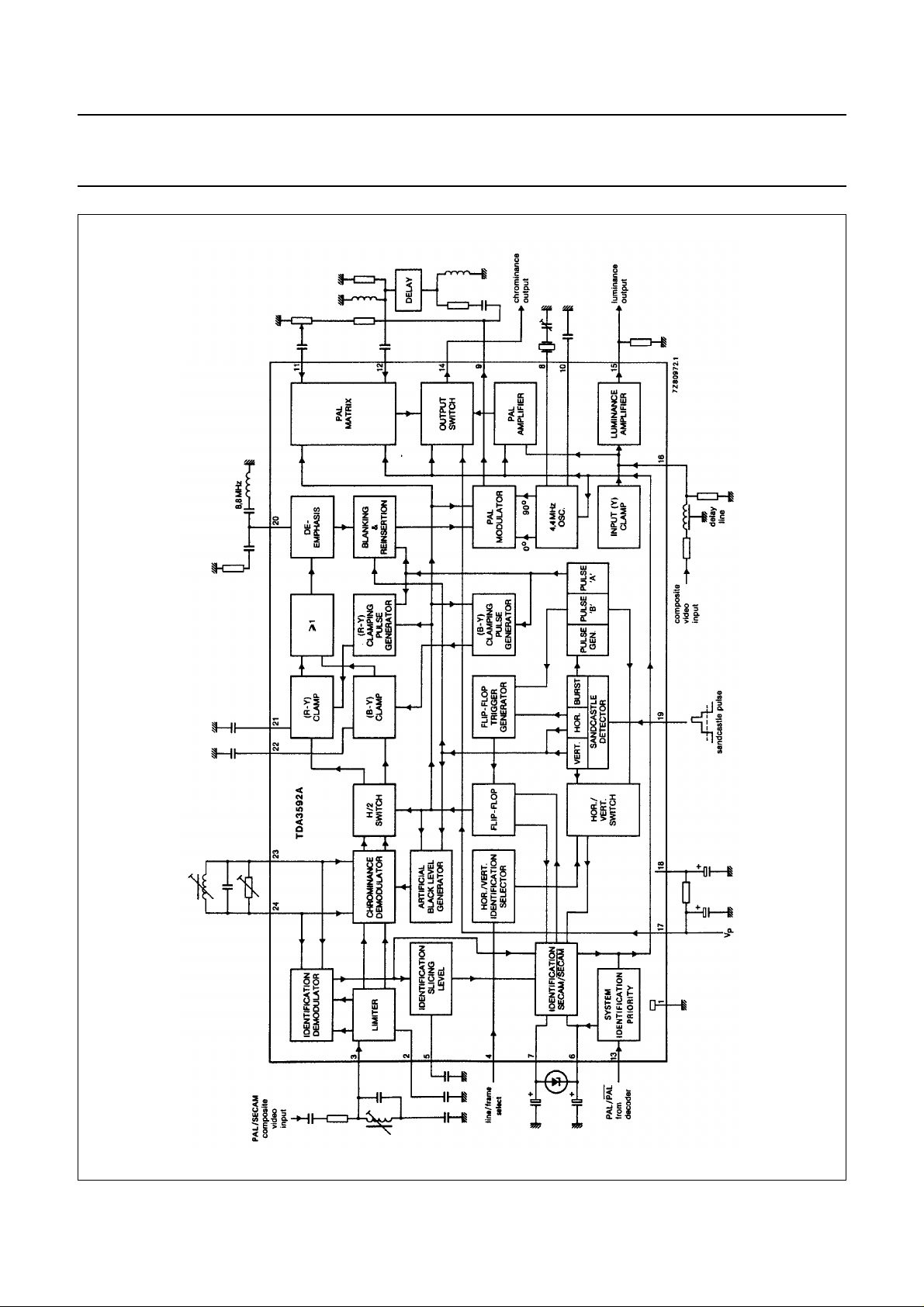
Fig.1 Block diagram.
Page 4

Philips Semiconductors Product specification
SECAM-PAL transcoder TDA3592A
PINNING
1. Ground.
2. Limiter feedback.
3. Limiter input: chrominance input SECAM; identification input SECAM/
4. Identification selection input using a DC level to preset the identification mode.
At V
< 2,9 V the TDA3592A is preset for frame identification.
4
> 4,1 V the TDA3592A is preset for line identification.
At V
4
5. Storage capacitor input for floating level identification.
6. Storage capacitor input to SECAM/
7. Double time-constant input to SECAM/
SECAM identification circuit.
SECAM identification circuit.
8. 4,43 MHz oscillator.
9. Sequentially modulated output.
10. Decoupling capacitor for miller integrator feedback circuit.
11. Direct input chrominance signal.
12. Delayed input chrominance signal.
13. PAL/PAL input signal from PAL decoder.
14. Chrominance output signal.
15. Luminance output signal.
16. Luminance/
17. Positive supply voltage (V
SECAM input signal.
).
p
18. Decoupled positive supply voltage.
19. Three-level sandcastle pulse input.
20. De-emphasis circuit connection: R = 560 Ω; C = 1 nF.
21. Storage capacitor connection for (R−Y) clamp.
22. Storage capacitor connection for (B−Y) clamp.
23. Demodulator reference tuned circuit: nominal frequency = 4,33 MHz; nominal QL= 2,45.
24. As for pin 23.
SECAM.
FUNCTIONAL DESCRIPTION
Demodulation
The chrominance and identification demodulators of the TDA3592A both share the same reference tuned circuit (pins 23
and 24). The identification circuit automatically detects whether the incoming signal is SECAM or SECAM (NTSC, PAL
or black-and-white).
When the incoming signals are PAL they are diverted via pin 16 to the chrominance output at pin 14 and no signal
demodulation takes place. The delay line connected to pin 16 delays the signals to equalize the delay of the SECAM-PAL
transcoding process. When SECAM signals are received, the PAL signal path is switched off.
Incoming SECAM signals are applied to pin 3 via an external bell filter. The signals are amplified, limited and then
demodulated. Only one demodulator is necessary as the colour difference signals are available sequentially. After
demodulation the colour difference signals are separated by an H/2 switch and then applied to (R-Y) and (B-Y) clamp
circuits where the black levels are clamped to the same DC level. With all conditions at pin 4, artificial black levels are
inserted during the horizontal blanking periods. This is done because of the possibility of horizontal burst signals not
being available. The artificial levels may not be identical to the detected black level due to circuit spread but this can be
corrected by detuning the reference tuned circuit.
January 1988 4
Page 5

Philips Semiconductors Product specification
SECAM-PAL transcoder TDA3592A
The two colour difference signals are combined again after clamping and then applied to the modulator via de-emphasis,
blanking and reinsertion circuits. The ratio of (R-Y) to (B-Y) at the de-emphasis output (pin 20) is 1,78.
Modulation
A burst signal is reinserted into the combined SECAM signal at the input to the PAL modulator. At this input the phase
relationship for magenta colour is +(R-Y) and−(B-Y). The modulation carriers for the (R-Y) and (B-Y) signals are 90° out
of phase; for a magenta colour the modulated (R-Y) component has the same phase position as the (R-Y) burst. The
(B-Y) burst is modulated 180° out of phase with respect to the (B-Y) component of a magenta-coloured input signal.
Identification SECAM/SECAM
Identification of the SECAM signal is performed using the fact that only SECAM signals have a line-to-line difference in
voltage level. The identification circuit compares the phase of the demodulated voltage difference waveform with the
phase of the flip-flop output. If the phase relationship is not correct, the flip-flop is reset by an extra pulse from the flip-flop
trigger generator. For horizontal identification the phase comparison is performed during the period of pulse ‘B’ (see
Fig.2). When vertical identification is selected, the comparison is performed only during the horizontal scan of the vertical
blanking. The SECAM identification circuits operate when selected by the voltage on pin 4; this may be horizontal, vertical
or combined horizontal and vertical identification, depending on the switching arrangements of pin 4.
These are as follows:
• Horizontal identification preset when V
• Vertical identification preset when V
• Horizontal/vertical combination when sandcastle pulse is present on pin 4.
4-1
< 2,9 V;
4-1
> 4,1 V;
Information obtained from the identification detector is also used for colour killing and, if required, for switching to PAL.
January 1988 5
Page 6
Philips Semiconductors Product specification
SECAM-PAL transcoder TDA3592A
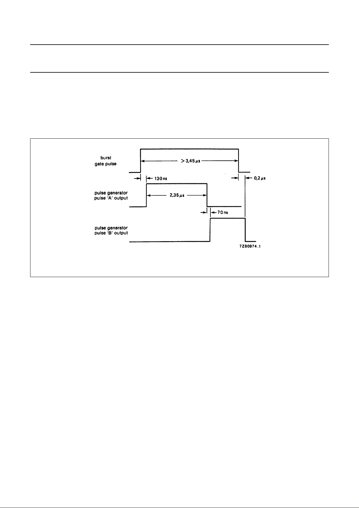
Sandcastle pulse detection
The sandcastle pulse detector requires a three-level sandcastle pulse to provide horizontal blanking, vertical blanking
and burst gate pulses. The detector burst gate pulse triggers a pulse generator which produces two timing pulses, pulse
‘A’ and pulse ‘B’ (see Fig.2). Pulse ‘A’ is used to time the PAL modulator burst and to sample the (R-Y) and (B-Y)
clamping pulse generators. A (R-Y) clamping pulse is generated only during a red line and a (B-Y) clamping pulse only
during a blue line. Pulse ‘B’ times the SECAM horizontal identification.
Fig.2 Burst gate timing pulse generation.
Carrier generation
The carrier signal for the PAL modulator is obtained from a 4,43 MHz oscillator. An internal Miller integrator operates in
conjunction with the decoupling capacitor at pin 10 to provide the required 90° phase shift.
PAL matrix
The signal output from the PAL modulator at pin 9 is sequentially modulated with (R-Y) burst phased in the +(R-Y)
direction, and (B-Y) burst phased in the −(B-Y) direction. This PAL signal is applied directly to pin 11 and via a 64 µs
delay to pin 12. A true PAL signal is constructed in the PAL matrix by means of an additional/substraction process (in a
correct H/2 sequence) using the delayed and undelayed inputs.
January 1988 6
Page 7

Philips Semiconductors Product specification
SECAM-PAL transcoder TDA3592A
Coupling of identification systems
Coupling of a TDA3592A and a PAL decoder can be performed to obtain an optimum identification system. The system
operates using the functions of pins 13, 6 and 7: the voltage level at pin 13 is controlled by the PAL/PAL detection of the
PAL decoder; and the voltage level at pins 6 and 7 are functions of SECAM/SECAM detection in the TDA3592A.
The circuit action is as follows and is summarized in Table 1.
Channel switching During channel switching pin 6 is taken rapidly to a high voltage (± 10,2 V), this corresponds
to the
SECAM mode of the TDA3592A.
PAL The high voltage level at pin 6 caused by channel switching is maintained by the TDA3592A
when it recognizes the signal as
signals are present). The PAL decoder recognizes the signal as PAL and takes pin 13 of
TDA3592A to a voltage greater than 1,7 V. The TDA3592A is now held in the SECAM
condition by an internal current source at pin 6.
SECAM The initial high voltage level (+ 10,2 V) at pin 6 caused by channel switching sets the
TDA3592A in the
This causes a voltage at pin 13 of < 1,1 V which prevents the internal current source of
TDA3592A maintaining the high voltage level of pin 6 which, in turn, allows the TDA3592A to
detect SECAM. The initiation of SECAM detection is delayed by the action of the external
circuit at pins 6 and 7 and commences as pin 6 approaches 7,0 V. The SECAM signals are
converted by TDA3592A to PAL signals at pin 14, which results in the PAL decoder switching
to the PAL mode (the TDA3592A remains in the SECAM mode).
Black-and-white The TDA3592A is initially set in the
detects P AL and the TDA3592A detects SECAM which results in a system operation in the
colour-killing mode.
SECAM mode and during this time the PAL decoder detects a PAL signal.
SECAM (this condition is maintained even if reflected PAL
SECAM mode as previously described. The P AL decoder
Table 1 System operating modes
TDA3592A PAL DECODER MODE SYSTEM OPERATING MODE
SECAM PAL SECAM
SECAM
SECAM PAL PAL
SECAM PAL black-and-white
System priorities
When TDA3592A pin 13 is connected to the PAL/
identification. Connecting TDA3592A pin 13 to ground will give SECAM priority.
Luminance and chrominance signal paths
The signal input at pin 16 is clamped by a circuit which detects the top of the luminance signal sync pulse. This clamp,
the luminance signal path to pin 15 and the
(typ.) 5 V. At this level of supply voltage the SECAM processing circuits are switched off, giving a reduction in total power
dissipation.
PAL condition not used
PAL output of a PAL decoder, the system will give PAL priority in signal
SECAM signal path to pin 14 remain active when the supply voltage falls to
January 1988 7
Page 8

Philips Semiconductors Product specification
SECAM-PAL transcoder TDA3592A
RATINGS
Limiting values in accordance with the Absolute Maximum System (IEC 134)
PARAMETER SYMBOL MIN. MAX. UNIT
Supply voltage (pin 17) V
Total power dissipation P
Operating ambient temperature range T
Storage temperature range T
P
tot
amb
stg
CHARACTERISTICS
V
P=V17−1
= 12 V; T
=25°C; unless otherwise specified.
amb
The parameter values are valid only when the reference tuned circuit has been aligned as detailed in note 1. All
voltages are reference to ground pin 1.
PARAMETER CONDITIONS SYMBOL MIN. TYP. MAX. UNIT
Supplies
Supply voltage (pin 17) V
Supply current (pin 17) I
Supply current (pin 18) I
Decoupled supply voltage (pin 18) R
ext17−18
=2 kΩ V
External capacitance (pin 18) C
Total power dissipation P
17
17
18
18
18
tot
9,0 12 13,2 V
65 90 115 mA
40 − 160 µA
8,8 11,8 13,2 V
−− 10 µF
− 1,08 1,38 W
Thermal resistance,
junction to ambient R
th j-a
− 40 45 K/W
Chrominance amplifier and
demodulator
Input signal SECAM
(peak-to-peak value) V
3(p-p)
−− 1100 mV
Input signal SECAM at which
correct limiting occurs
(peak-to-peak value) V
Input resistance (pin 3) R
Input capacitance (pin 3) C
3(p-p)
3
3
15 100 300 mV
9,6 12,1 14,6 kΩ
−− 5pF
Input resistance between
pins 23 and 24 R
23−24
2,9 3,6 4,3 kΩ
Input capacitance between
pins 23 and 24 C
23−24
− 12 − pF
De-emphasis output resistance
(pin 20) R
20
0,9 1,1 1,3 kΩ
Chrominance demodulator
zero point stability (pin 20) note 2 f
0
− 5 − kHz
− 13,2 V
− 1,78 W
−25 +70 °C
−25 +150 °C
January 1988 8
Page 9

Philips Semiconductors Product specification
SECAM-PAL transcoder TDA3592A
PARAMETER CONDITIONS SYMBOL MIN. TYP. MAX. UNIT
Linearity of (B-Y) demodulation
(pin 20) note 3 −−94 − %
Linearity of (R-Y) demodulation
(pin 20) note 4 −−100 − %
(R-Y)/(B-Y) ratio (pin 20) −−1,78 − %
Relative deviation of reinserted
black level/demodulated black
level (pin 20) as a function of
temperature
(R-Y) signals note 5 −−0,22 − kHz/°C
(B-Y) signals note 5 −−0,22 − kHz/°C
Identification SECAM/
SECAM
Input voltage for line
identification (pin 4) V
Input voltage for frame
identification (pin 4) V
Switching level for line/frame
identification (pin 4) V
Input current (pin 4) −I
Voltage at pin 6 during
SECAM/PAL V
Voltage at pin 6 during
SECAM/PAL V
Voltage at pin 6 during SECAM V
Identification at pin 6 V
Colour OFF for SECAM V
Colour ON for SECAM V
Slicing level reference voltage
(pin 5) V
Sandcastle pulse detector and
clamping pulse generator
Voltage level at which the
vertical blanking pulse is
separated V
Voltage level at which the
horizontal blanking pulse is
separated V
Voltage level at which the burst
gating pulse is separated V
note 6
4
4
4
4
6
6
6
6
6
6
5
19
19
19
4,1 − V
0 − 2,9 V
3,0 3,5 4,0 V
− 525µA
− 10,2 − V
− 11,5 − V
− 7,0 − V
− 10,6 − V
9,8 10,1 10,4 V
8,8 9,1 9,4 V
− 8,4 − V
1,0 1,5 2,0 V
3,0 3,5 4,0 V
6,5 7,0 7,5 V
V
P
January 1988 9
Page 10

Philips Semiconductors Product specification
SECAM-PAL transcoder TDA3592A
PARAMETER CONDITIONS SYMBOL MIN. TYP. MAX. UNIT
Input current V19=0V −I
19
Width of pulse ‘A’ (Fig.2) note 7 1,85 2,35 2,85 µA
Required width of pulse ‘B’
(Fig.2) note 7 0,6 −−µs
Luminance amplifier
Input signal (peak-to-peak value)
(pin 16) V
Gain (pin 16 to 15) f
= 4,4 MHz G
16
Input current (pin 16) I
Output impedance (pin 15) Z
16(p-p)
16−15
16
15
Frequency response at −3 dB
(pin 15 and 16) f 6,0 −−MHz
Gain (pin 16 to 14) f
= 4,4 MHz G
16
16−14
Frequency response at −3 dB
(pin 14 and 16) f 6,0 −−MHz
External load resistance (pin 15) R
L
Limiter, chrominance
demodulator and PAL
modulator
Output resistance (pin 9) R
note 8
9
DC output voltage during
horizontal blanking (pin 9) V
9
Internal biasing resistor for
emitter follower (pin 9) − 9,0 − kΩ
External load resistance (pin 9) R
L(9)
Output signal (pin 9) when input
to pin 3 has a ∆f of 280 kHz;
without external load
(peak-to-peak value) V
9(p-p)
(R-Y)/(B-Y) ratio (pin 9) 1,50 1,78 2,11
Chrominance/burst ratio for
SECAM (pin 9) 2,5 3,0 3,5
Linearity of (B-Y) signal (pin 9) note 3 85 92 99 %
Linearity of (R-Y) signal (pin 9) note 4 93 100 107 %
Black level shift as a function of
temperature (pin 9)
(R-Y) signals note 9 − 0,22 − kHz/°C
(B-Y) signals note 9 − 0,22 − kHz/°C
− 30 100 µA
− 1,2 1,7 V
6,5 7,5 8,5 dB
− 1,0 5,0 µA
− 20 −Ω
6,0 7,0 8,0 dB
2,0 −−kΩ
− 25 −Ω
− 9,6 − V
2 −−kΩ
− 0,82 − mV
January 1988 10
Page 11

Philips Semiconductors Product specification
SECAM-PAL transcoder TDA3592A
PARAMETER CONDITIONS SYMBOL MIN. TYP. MAX. UNIT
Phase relationship of modulated
(R-Y) burst to modulated
(B-Y) burst (pin 9) 87 90 93 deg
Amplitude relationship of
modulated (R-Y) burst to
modulated (B-Y) burst (pin 9) −1,5 0 +1,5 dB
Black level shift as a function of
supply voltage (pin 9)
(R-Y) signal −−1,5 − kHz/V
(B-Y) signal − 1,0 − kHz/V
Oscillator
Oscillator frequency (pin 9)
(set with series capacitor) f
OSC
Frequency deviation without
spread of external components
(pin 9) ∆f
OSC
Temperature coefficient of
oscillator frequency (pin 9) −−2 −3 Hz/°C
Frequency deviation for change
of V
from 9,0 to 13,2 V ∆f
P
DC voltage (pin 8) V
Input resistance (pin 8) R
DC voltage (pin 10) V
Input resistance (pin 10) R
OSC
8
8
10
10
PAL matrix
Input resistance (pin 11) R
Input resistance (pin 12) R
11
12
Output resistance (pin 14)
(SECAM/SECAM) R
14
Internal emitter follower load
resistance (pin 14) R
External load resistor (pin 14) R
DC voltage (pin 11) V
DC voltage (pin 12) V
DC voltage (pin 14) SECAM mode V
DC voltage (pin 14)
SECAM mode
INT(14)
L(14)
11
12
14
and
line blanking V
14
− 4,433619 − MHz
−− ±150 Hz
−− 150 Hz
− 4,7 − V
− 1 − kΩ
− 4,4 − V
− 2 − kΩ
700 900 1100 Ω
700 900 1100 Ω
− 40 −Ω
− 7 − kΩ
2,4 −−kΩ
− 5,0 − V
− 5,0 − V
− 6,2 − V
− 4,9 − V
January 1988 11
Page 12

Philips Semiconductors Product specification
SECAM-PAL transcoder TDA3592A
PARAMETER CONDITIONS SYMBOL MIN. TYP. MAX. UNIT
H/2 ripple on chrominance
output (pin 14)
(peak-to-peak value) SECAM mode V
Gain A; pin 11 to 14 G
14(p-p)
A
Gain B; pin 12 to 14
((R-Y) at pin 9) G
B
Gain C; pin 12 to 14
((B-Y) at pin 9) G
Gain A − gain B G
Gain A − gain C G
Gain B − gain C G
C
A−GB
A−GC
B−GC
Phase A; pins 11, 14 to
pins 12, 14 ((R-Y) at pin 9) − 181,5 − deg
Phase B; pins 11, 14 to
pins 12, 14 ((B-Y) at pin 9) − 1,5 − deg
Phase A − phase B 178 180 182 deg
−− 100 mV
910 11dB
910 11dB
910 11dB
−0,7 −+0,7 dB
−0,7 −+0,7 dB
−0,7 −+0,7 dB
Identification PAL/
PAL
Input condition for PAL (pin 13) V
Input condition for
Input current V
Input resistance V
PAL (pin 13) V
=6 V I
13
= 8,2 V R
13
Pin 6 internal current in
PAL/SECAM mode −I
Switching level PAL/
PAL
(pin 13) V
13
13
13
13
6
13
1,7 − V
−− 1,1 V
−− 10 µA
7,5 11,5 15,5 kΩ
0,24 0,4 0,58 mA
1,2 1,4 1,6 V
V
P
January 1988 12
Page 13

Philips Semiconductors Product specification
SECAM-PAL transcoder TDA3592A
CHARACTERISTICS AT LOW SUPPLY VOLTAGE
V
P=V17−1
= 5 V; T
PARAMETER CONDITIONS SYMBOL MIN. TYP. MAX. UNIT
Supplies
Supply current I
Supply voltage switching level for
preset SECAM signal path SECAM processing
Luminance amplifier
Input signal (peak-to-peak value) V
Gain (pin 16 to 15) f
Input current (pin 16) I
Output impedance (pin 15) |Z
Minimum load resistance (pin 15) R
Frequency response at −3 dB
(pin 16 to 15) f 6,0 −−MHz
Gain (pin 16 to 14) f
Frequency response at −3 dB
(pin 16 to 14) f 6 −−MHz
=25°C; unless otherwise specified
amb
OFF V
= 4,4 MHz G
16
= 4,4 MHz G
16
17+I18
17−1
16(p-p)
16−15
16
| − 20 −Ω
15−1
L
16−14
16 20 24 mA
6,5 7,5 8,2 V
− 0,45 0,56 V
6,0 7,0 8,0 dB
− 1,0 5,0 µA
2 −−kΩ
5,7 6,8 7,9 dB
January 1988 13
Page 14

Philips Semiconductors Product specification
z
SECAM-PAL transcoder TDA3592A
Notes to the characteristics
1. The parameter values given in the characteristics are valid only when the following alignment procedure is
performed:
a) Supply a SECAM signal input to pin 3 at 100 mV (peak-to-peak value) without deviation during a red and blue
line (SECAM black colour information).
b) Align the reference tuned circuit so that the output signal from pin 14 to the PAL decoder is minimum during scan
(PAL black colour information).
2. When the input signal to the limiter (pin 3) changes from 300 to 15 mV (peak-to-peak value) the zero point of the
chrominance demodulator shifts by a typical value of 5 kHz; f = 4,33 MHz (typ.).
3. (B-Y) linearity is defined by V
4. (R-Y) linearity is defined by V
out(yellow)/Vout(blue)
out(cyan)/Vout(red)
where f
where f
= (typ.) 4,02 MHz; f
yellow
= (typ.) 4,68 MHz; f
cyan
= (typ.) 4,48 MHz.
blue
= (typ.) 4,12 MHz.
red
5. The parameter value is equated by:
E
E1 E2–
=
--------------------2
F
F1 F2–
=
-------------------2
BD–()FA( C)E⁄––⁄
-----------------------------------------------------------------YX–
f kHz()∆
×
----------------------°C
Where
A = demodulated black level at temperature X
B = demodulated black level at temperature Y
C = artificial black level at temperature X
D = artificial black level at temperature Y
E1 = demodulated output signal at temperature X (f
o
−∆f)
E2 = demodulated output signal at temperature X (fo+∆f)
F1 = demodulated output signal at temperature Y (fo−∆f)
F2 = demodulated output signal at temperature Y (fo+ ∆f)
for B-Y: fo= fob= 4,25 MHz (∆f = 230 kHz)
for R-Y: fo= for= 4,40625 MHz (∆f = 280 kHz)
6. During stable signal conditions V7 is always at VF(BAT85) below V6.
7. The burst gate pulse width > 3,45 µs.
8. The specification figures are only valid when the reference tuned circuit is aligned as indicated in note 1.
9. Ensure that the 4,433 MHz carrier is in the correct phase; black level shift at temperature X = A and at Y = B.
Output signal (∆f = 230 kHz for B-Y; ∆f = 280 kHz for R-Y) at temperature X = E and at Y = F.
The parameter is equated by:
BFB–()⁄[]AEA–()⁄[]–
---------------------------------------------------------------------------- YX–
×
230; 280 kH
10. Chrominance definition − burst ratio at SECAM condition (pin 9).
The parameter is equated by:
V
out p p–()
-----------------------------------------------------------V
Red R Y–()
burst p p–()
RY–()
.
January 1988 14
Page 15

Philips Semiconductors Product specification
SECAM-PAL transcoder TDA3592A
APPLICATION INFORMATION
January 1988 15
Fig.3 Application circuit.
= line identification
P
= sandcastle = line + frame identification
= ground = frame identification
= V
4−1
4−1
4−1
V
V
(1) V
(2) minimum load resistance at pin 15 = 2 kΩ
Page 16

Philips Semiconductors Product specification
SECAM-PAL transcoder TDA3592A
PACKAGE OUTLINE
DIP24: plastic dual in-line package; 24 leads (600 mil)
D
seating plane
L
Z
24
pin 1 index
e
b
SOT101-1
M
E
A
2
A
A
1
w M
b
1
13
E
c
(e )
1
M
H
1
0 5 10 mm
scale
DIMENSIONS (inch dimensions are derived from the original mm dimensions)
A
A
A
UNIT
inches
Note
1. Plastic or metal protrusions of 0.25 mm maximum per side are not included.
max.
mm
OUTLINE
VERSION
SOT101-1
1 2
min.
max.
1.7
1.3
0.066
0.051
IEC JEDEC EIAJ
051G02 MO-015AD
b
b
1
0.53
0.38
0.021
0.015
0.32
0.23
0.013
0.009
REFERENCES
cD E e M
32.0
31.4
1.26
1.24
January 1988 16
12
14.1
13.7
0.56
0.54
(1)(1)
e
L
3.9
3.4
EUROPEAN
PROJECTION
M
15.80
15.24
0.62
0.60
E
17.15
15.90
0.68
0.63
1
0.15
0.13
H
w
0.252.54 15.24
0.010.10 0.60
ISSUE DATE
92-11-17
95-01-23
Z
max.
2.25.1 0.51 4.0
0.0870.20 0.020 0.16
(1)
Page 17

Philips Semiconductors Product specification
SECAM-PAL transcoder TDA3592A
SOLDERING
Introduction
There is no soldering method that is ideal for all IC
packages. Wave soldering is often preferred when
through-hole and surface mounted components are mixed
on one printed-circuit board. However, wave soldering is
not always suitable for surface mounted ICs, or for
printed-circuits with high population densities. In these
situations reflow soldering is often used.
This text gives a very brief insight to a complex technology.
A more in-depth account of soldering ICs can be found in
“IC Package Databook”
our
Soldering by dipping or by wave
The maximum permissible temperature of the solder is
260 °C; solder at this temperature must not be in contact
DEFINITIONS
Data sheet status
Objective specification This data sheet contains target or goal specifications for product development.
Preliminary specification This data sheet contains preliminary data; supplementary data may be published later.
Product specification This data sheet contains final product specifications.
(order code 9398 652 90011).
with the joint for more than 5 seconds. The total contact
time of successive solder waves must not exceed
5 seconds.
The device may be mounted up to the seating plane, but
the temperature of the plastic body must not exceed the
specified maximum storage temperature (T
printed-circuit board has been pre-heated, forced cooling
may be necessary immediately after soldering to keep the
temperature within the permissible limit.
Repairing soldered joints
Apply a low voltage soldering iron (less than 24 V) to the
lead(s) of the package, below the seating plane or not
more than 2 mm above it. If the temperature of the
soldering iron bit is less than 300 °C it may remain in
contact for up to 10 seconds. If the bit temperature is
between 300 and 400 °C, contact may be up to 5 seconds.
stg max
). If the
Limiting values
Limiting values given are in accordance with the Absolute Maximum Rating System (IEC 134). Stress above one or
more of the limiting values may cause permanent damage to the device. These are stress ratings only and operation
of the device at these or at any other conditions above those given in the Characteristics sections of the specification
is not implied. Exposure to limiting values for extended periods may affect device reliability.
Application information
Where application information is given, it is advisory and does not form part of the specification.
LIFE SUPPORT APPLICATIONS
These products are not designed for use in life support appliances, devices, or systems where malfunction of these
products can reasonably be expected to result in personal injury. Philips customers using or selling these products for
use in such applications do so at their own risk and agree to fully indemnify Philips for any damages resulting from such
improper use or sale.
January 1988 17
 Loading...