

Page 1

INTEGRATED CIRCUITS
DATA SH EET
TDA3567
NTSC decoder
Product specification
File under Integrated Circuits, IC02
June 1986
Page 2

Philips Semiconductors Product specification
NTSC decoder TDA3567
GENERAL DESCRIPTION
The TDA3567 is a monolithic integrated decoder for the NTSC colour television standards. It combines all functions
required for the demodulation of NTSC signals. Further more it contains a luminance amplifier, an RGB-matrix and
amplifier. These amplifiers supply output signals up to 5 V peak-to-peak (picture information) enabling direct drive of the
discrete output stages.
QUICK REFERENCE DATA
PARAMETER CONDITIONS SYMBOL MIN. TYP. MAX. UNIT
Supply voltage pin 1 VP=V
Supply current pin 1 I
Luminance input signal
pin 8
1-17
P=I1
Input voltage
(peak-to-peak value) V
8-17(p-p)
Contrast control range − 20 − dB
Chrominance amplifier
pin 3
Input voltage
(peak-to-peak value) V
3-17(p-p)
Saturation control range 50 −−dB
9 12 13,2 V
− 65 − mA
− 0,45 − V
− 550 − mV
RGB matrix and amplifiers
Output voltage at nominal
luminance input signal
and nominal contrast
(peak-to-peak value) V
Sandcastle input
pin 7
Blanking input voltage V
10,11,12-17(p-p)
7-17
4,0 5,0 6,0 V
1,0 1,5 2,0 V
Burst gating and clamping
input voltage V
7-17(p-p)
6,5 7,0 7,5 V
PACKAGE OUTLINE
18-lead DIL; plastic, with internal heatspreader (SOT102-1); SOT102-1; 1996 November 25.
June 1986 2
Page 3
Philips Semiconductors Product specification
NTSC decoder TDA3567
June 1986 3
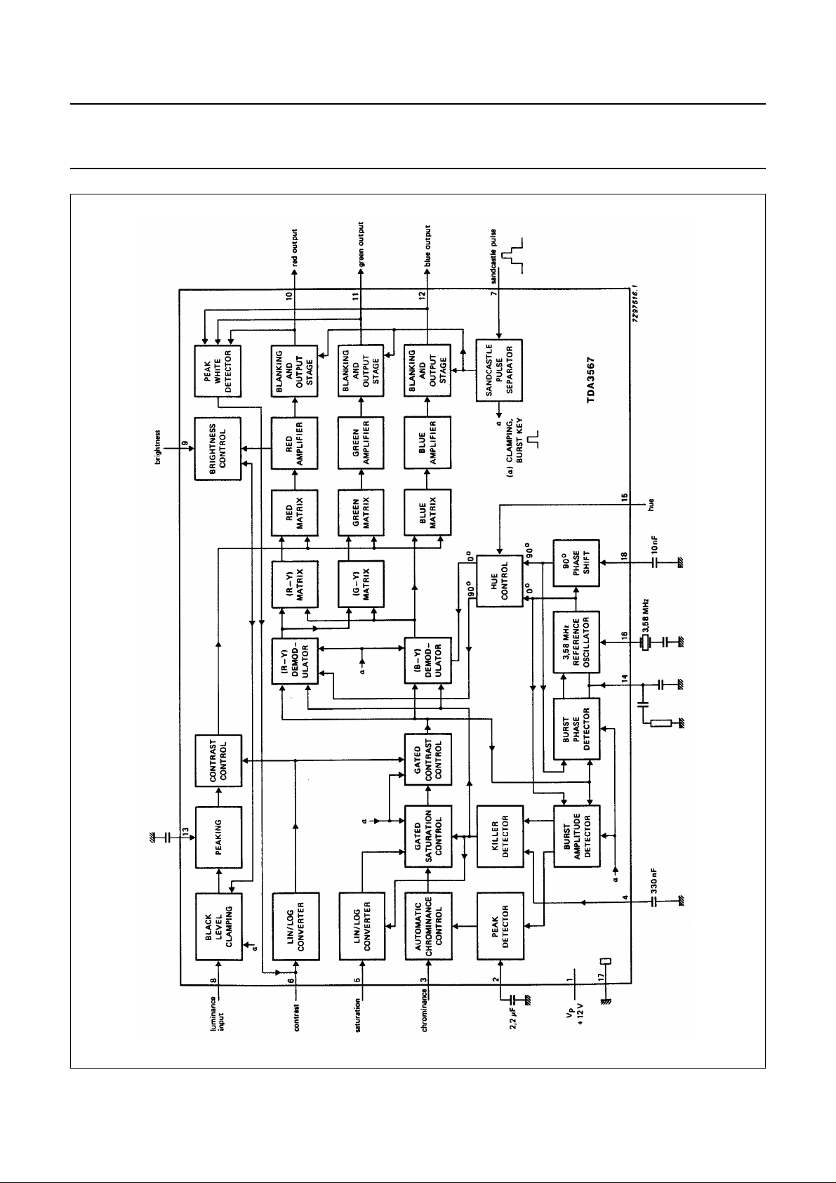
Fig.1 Block diagram.
Page 4

Philips Semiconductors Product specification
NTSC decoder TDA3567
FUNCTIONAL DESCRIPTION
Luminance amplifier
(1)
The luminance amplifier is voltage driven and requires an input signal of 450 mV peak-to-peak
line must be connected between the i.f. amplifier and the decoder. The input signal must be a.c. coupled to the input pin 8.
The black level clamp circuit of the RGB amplifiers uses the coupling capacitor as a storage capacitor. After clamping
the signal is fed to a peaking stage. The RC network connected to pin 13 is used to define the amount of overshoot.
The peaking stage is followed by a contrast control stage. The control voltage has to be supplied to pin 6. The control
voltage range is nominally −17 to + 3 dB. The linear curve of the contrast control voltage is shown in Fig.2.
Chrominance amplifier
The chrominance amplifier has an asymmetrical input. The input signal at pin 3 must be a.c. coupled, and must have an
amplitude of 550 mV peak-to-peak. The gain control stage has a control range in excess of 30 dB, the maximum input
signal should not exceed 1,1 V peak-to-peak, otherwise clipping of the input signal will occur. From the gain control stage
the chrominance signal is fed to the saturation and contrast control stages. Chrominance and luminance control stages
are directly coupled to obtain good tracking. The saturation is linearly controlled via pin 5. The control voltage range is
2 V to 4 V. The impedance is high and the saturation control range is in excess of 50 dB. The burst signal is not affected
by contrast or saturation control. After the amplification and control stages the chrominance signal is internally fed to the
(R-Y) and (B-Y) demodulators, burst phase and a.c.c. detectors.
The luminance delay
Oscillator and a.c.c. circuit
The 3,58 MHz reference oscillator operates at the subcarrier frequency. The crystal must be connected between pin 16
and ground. The oscillator does not require adjustment due to the small spreads of the IC. The free running frequency
of the oscillator can be checked by connecting the saturation control (pin 5) to the positive supply line. Then the loop is
opened, so that the frequency can be measured. The oscillator has an internal gain limiting stage which controls the gain
to unity, so that internal signals are sinusoidal. This prevents the generation of higher harmonics of the subcarrier signals.
The burst signal is compared to a 0° reference signal by the burst amplitude detector and is then amplified and fed to a
peak detector for a.c.c. and to a sample and hold circuit which drives the colour killer circuit. The reference signal for the
burst phase detector is provided by the 90° phase shifted signal. An RC network is used to obtain the required catching
range and noise immunity for the output voltage of the burst phase detector.
The hue control is obtained by mixing oscillator signals with a phase of 0° and 90° before they are fed to the (R-Y) and
(B-Y) demodulators. The 90°phase shifted signal is provided by a miller integrator (biased by pin 18). As the hue control
is independent of the PLL, the control will react without time delay on the control voltage changes.
Demodulator circuits
The demodulators are driven by the amplified and controlled chrominance signals, the reference signals are obtained
from the hue control circuit. In nominal hue control position the phase angle of (R-Y) reference signal is 0°, the phase
angle of the (B-Y) reference signal is 90°.
For flesh tone corrections the demodulated (R-Y) signal is matrixed with the demodulated (B-Y) signal according to the
following equations:
RY–()
matrixed
GY–()
matrixed
161R Y–()IN0– 42 B Y–()
,,=
043R Y–()IN0– 11 B Y–()
,,=
IN
IN
BY–()
matrixed
(1) Signal with negative going sync; amplitude includes sync pulse amplitude.
BY–()
=
IN
June 1986 4
Page 5

Philips Semiconductors Product specification
NTSC decoder TDA3567
In these equations (R-Y)IN and (B-Y)IN indicate the colour difference signal amplitudes, when the chrominance signal is
demodulated with a phase difference between the R-Y and B-Y demodulator of 90° and a gain ratio B-Y/R-Y = 1,78.
RGB matrix circuit and amplifiers
The three matrix and amplifier circuits are identical. The luminance signal and the colour difference signals are added in
the matrix circuit to obtain the colour signal.
Output signals are 5 V (peak-to-peak) (black-white) for the following nominal input signals and control settings.
• Luminance 450 mV (peak-to-peak)
• Chrominance 550 mV (peak-to-peak) (burst-to-chrominance ratio of the input 1 : 2.2)
• Contrast −3 dB (maximum)
• Saturation −10 dB (maximum)
The maximum available output voltage is approximately 7 V (peak-to-peak). The black level of the red channel is
compared with a variable external reference level (pin 9), which provides the brightness control. The control loop is
closed via the luminance input.
The luminance input is varied to control the black level control, therefore the green and blue outputs will follow any
variation of the red output. The output of the black control can be varied between 2 V to 4 V. The corresponding
brightness control voltage is shown in Fig.4.
If the output signal surpasses the level of 9 V the peak-white limiter circuit becomes active and reduces the output signal
via the contrast control.
Blanking of RGB signals
A slicing level of about 1,5 V is used for this blanking function, so that the wide part of the sandcastle pulse is separated
from the rest of the pulse. During blanking a level of + 2 V is available at the output.
June 1986 5
Page 6

Philips Semiconductors Product specification
NTSC decoder TDA3567
RATINGS
Limiting values in accordance with the Absolute Maximum System (IEC 134)
Supply voltage (pin 1) V
Total power dissipation P
Storage temperature range T
Operating ambient temperature range T
THERMAL RESISTANCE
P
tot
stg
amb
= V
1-17
max. 13,2 V
max. 1,7 W
−25 to + 150 ° C
−25 to + 65 ° C
From junction to ambient (in free air) R
th j-a
= 50 K/W
CHARACTERISTICS
V
P=V1-17
=12 V; T
=25°C; unless otherwise specified
amb
PARAMETER CONDITIONS SYMBOL MIN. TYP. MAX. UNIT
Supply
Supply voltage V
Supply current I
Total power dissipation P
P=V1-17
P=I1
tot
9 12 13,2 V
− 65 − mA
− 0,78 − W
Luminance input signal
Input voltage note 1
(peak-to-peak value) pin 8 V
8-17(p-p)
− 450 − mV
Input voltage level before
clipping occurs in the
input stage V
Input current I
8-17
8
−−1V
− 0,15 1,0 µA
Contrast control range see Fig.2 −17 −+3dB
Input current contrast
control for V
< 6V I
6-17
7
− 0,5 15 µA
Input current when the
peak-white limiter
is active V
Input resistance V
= 2,5 V I
6-17
> 6V R
6-17
7
7-17
− 5,5 − mA
1,4 2,0 2,6 kΩ
Peaking of luminance signal
Output impedance pin 13 |Z
| − 200 −Ω
13-17
Ratio of internal/external
current when pin 13 is
short-circuited − 3 −
June 1986 6
Page 7

Philips Semiconductors Product specification
NTSC decoder TDA3567
PARAMETER CONDITIONS SYMBOL MIN. TYP. MAX. UNIT
Chrominance amplifier
Input signal amplitude note 2
(peak-to-peak value) pin 3 V
3-17(p-p)
Input signal amplitude
before clipping occurs
in the input stage
(peak-to-peak value) V
3-17(p-p)
Minimum burst signal
amplitude within the
a.c.c. control range
(peak-to-peak) 35 −−mV
A.C.C. control range 30 −−dB
Change of the burst signal
at the output for the
complete control range ∆V −−+1dB
Input impedance pin 3 |Z
Input capacitance pin 3 C
|6810kΩ
3-17
3-17
Saturation control range see Fig.3 50 −−dB
Input current saturation
control for V
Input impedance V
5-17
to 10 V |Z
> 6V I
5-17
=6V
5
| 1,4 2,0 2,6 kΩ
5-17
Input impedance when the
colour killer is active |Z
Input impedance for V
> 10 V |Z
5-17
| 1,4 2,0 2,6 kΩ
5-17
| 0,7 1,0 1,3 kΩ
5-17
Tracking between luminance
and chrominance contrast for 10 dB of
control − 12dB
Cross coupling between
luminance and
chrominance amplifier note 4 −−50 −46 dB
− 550 − mV
−−1,1 V
− 46pF
− 120µA
June 1986 7
Page 8

Philips Semiconductors Product specification
NTSC decoder TDA3567
PARAMETER CONDITIONS SYMBOL MIN. TYP. MAX. UNIT
Reference part
Phase locked loop
Catching range ∆ f ± 400 ± 500 − Hz
Phase shift for 400 Hz
deviation of the carrier
frequency ∆−−5 deg
Oscillator
Temperature coefficient of
oscillator frequency TC
Frequency deviation ∆ V
= ± 10% ∆ f
P
Input resistance pin 16 R
Input capacitance pin 16 C
osc
osc9
16-17
22-17
A.C.C. generation
Voltage at pin 4 nominal
input signal V
4-17
Voltage at pin 4 without
burst input V
Colour-off voltage V
Colour-on voltage V
4-17
4-17
4-17
Change in burst amplitude
with temperature − 0,1 − %/K
Change in burst amplitude
with 10% supply
voltage change − 0 − %/V
Voltage at pin 2 at
nominal input signal V
2-17
Hue control
Control voltage range see Fig.5
Input current for V
Input impedance for V
< 5V I
15-17
> 5V |Z
15-17
14
| 1,5 2,5 3,5 kΩ
14-17
− 1,5 2,5 Hz/K
− 150 250 Hz
260 360 460 Ω
−−10 pF
− 4,0 − V
− 1,9 − V
− 2,5 − V
− 2,8 − V
− 5,0 − V
− 0,5 20 µA
June 1986 8
Page 9

Philips Semiconductors Product specification
NTSC decoder TDA3567
PARAMETER CONDITIONS SYMBOL MIN. TYP. MAX. UNIT
Demodulation part
Ratio of demodulation
signals (measured at the
various outputs) note 7
(R-Y)/(B-Y); no (R-Y) signal −−0,42 −
(R-Y)/(B-Y); colour bar signal − 1,4 −
V
10 17–
-----------------V
12 17–
V
10 17–
-----------------V
12 17–
(G-Y)/(R-Y); no (B-Y) signal −−0,25 −
(G-Y)/(B-Y); no (R-Y) signal −−0,11 −
V
11 17–
-----------------V
12 17–
V
11 17–
-----------------V
12 17–
Frequency response 0 to 0,7 MHz −−−3dB
RGB matrix and amplifier
Output signal amplitude at nominal
V
10,11,12-17(p-p)
4,0 5,0 6,0 V
luminance input
signal and nominal
contrast (peak-topeak value)
note 3
black-white
Output signal amplitude of the
“blue” channel
at nominal
contrast and
V
12-17(p-p)
− 3,8 − V
saturation control
setting and no
luminance signal
to the input (B-Y)
signal (peak-topeak value)
Maximum peak-white level note 6 V
Maximum output current I
10,11,12-7
10,11,12-17
9,0 9,3 9,6 V
−−10 mA
Difference in the black
level between the
−−600 mV
three channels
Black level shift with
vision content − 10 40 mV
Brightness control voltage
range see Fig.4
June 1986 9
Page 10

Philips Semiconductors Product specification
V
V
NTSC decoder TDA3567
PARAMETER CONDITIONS SYMBOL MIN. TYP. MAX. UNIT
Brightness control input
current I
9
Black level variation with
temperature V/T − 0,15 1,0 mV/K
Black level variation with
contrast control ∆V − 75 200 mV
Relative spread between the
three output signals −−10 %
Relative variation in black
level between the
three channels
during variations
of contrast
(10 dB), brightness
∆V − 020mV
(± 1 V), and
supply voltage
(± 10%)
Differential drift of black
level over a temperature
∆V − 020mV
range of 40 °C
Blanking level at the RGB
outputs V
Tracking of output black levels
with supply voltage
b1
∆
------------ V
b1
b1
p
×
---------V∆
p
−−−50 µA
1,95 2,15 2,35 V
1,0 1,05 1,1
Signal-to-noise ratio of
output signals note 5 S/N 62 −−dB
Residual 3,58 MHz in RGB
outputs (peak-to-peak
value) V
R(p-p)
− 50 75 mV
Residual 7,1 MHz and higher
harmonics in the RGB
V
R(p-p)
− 50 75 mV
outputs (peak-to-peak
value)
RGB output impedance |Z
10,11,12-17
| −−50
Frequency response of total
luminance and RGB
0 to 5 MHz −−−3dB
amplifier circuits
June 1986 10
Page 11

Philips Semiconductors Product specification
NTSC decoder TDA3567
PARAMETER CONDITIONS SYMBOL MIN. TYP. MAX. UNIT
Sandcastle input
Level at which the RGB
blanking is activated V
7-17
Level at which burst gate
clamping pulses are
V
7-17
separated
Delay between black level
clamping and burst
t
d
gating pulse
Input currents V
= 0 to 1 V I
7-17
= 1 to 8,5 V I
V
7-17
V
= 8,5 to 12 V I
7-17
7
7
7
Notes to the characteristics
1. Signal with negative going sync; amplitude includes sync pulse amplitude.
2. Indicated is a signal for colour bar with 75% saturation, so the chrominance to burst ratio is 2,2 : 1.
3. Nominal contrast is specified as maximum contrast −3 dB and nominal saturation as maximum saturation −10 dB.
4. Cross coupling is measured under the following condition:
- input signals nominal;
- contrast and saturation such that nominal output signals are obtained;
- the signals at the output at which no signal should be available must be compared with the nominal output signal
at that output.
5. The signal-to-noise ratio is specified as peak-to-peak signal with respect to RMS noise.
6. When this level is exceeded the amplifier of the output signal is reduced via a discharge of the capacitor on pin 7
(contrast control). Discharge current is 5,5 mA.
7. These matrixed values are found by measuring the ratio of the various output signals. The values are derived from
the matrix equations given in the section ‘FUNCTIONAL DESCRIPTION’.
1,0 1,5 2,0 V
6,5 7,0 7,5 V
300 375 450 ns
−−−1mA
−−20 −40 µA
−−2mA
June 1986 11
Page 12

Philips Semiconductors Product specification
NTSC decoder TDA3567
Fig.2 Contrast control voltage range. Fig.3 Saturation control voltage range.
Fig.4 Brightness control voltage range. Fig.5 Hue control voltage range.
June 1986 12
Page 13

Philips Semiconductors Product specification
NTSC decoder TDA3567
APPLICATION INFORMATION
Fig.6 Application diagram.
June 1986 13
Page 14

Philips Semiconductors Product specification
NTSC decoder TDA3567
PACKAGE OUTLINES
DIP18: plastic dual in-line package; 18 leads (300 mil)
D
seating plane
L
Z
18
pin 1 index
e
b
SOT102-1
M
E
A
2
A
A
1
w M
b
1
b
2
10
E
c
(e )
1
M
H
1
0 5 10 mm
scale
DIMENSIONS (inch dimensions are derived from the original mm dimensions)
A
A
A
UNIT
max.
mm
inches
Note
1. Plastic or metal protrusions of 0.25 mm maximum per side are not included.
OUTLINE
VERSION
SOT102-1
12
min.
max.
IEC JEDEC EIAJ
b
1.40
1.14
0.055
0.044
b
1
0.53
0.38
0.021
0.015
b
cD E e M
2
0.32
1.40
0.23
1.14
0.013
0.055
0.009
0.044
REFERENCES
21.8
21.4
0.86
0.84
June 1986 14
9
(1) (1)
6.48
6.20
0.26
0.24
L
e
1
M
3.9
8.25
3.4
7.80
0.15
0.32
0.13
0.31
EUROPEAN
PROJECTION
E
0.37
0.33
H
9.5
8.3
w
max.
0.2542.54 7.62
0.854.7 0.51 3.7
0.010.10 0.30
0.0330.19 0.020 0.15
ISSUE DATE
93-10-14
95-01-23
(1)
Z
Page 15

Philips Semiconductors Product specification
NTSC decoder TDA3567
SOLDERING
Introduction
There is no soldering method that is ideal for all IC packages. Wave soldering is often preferred when through-hole and
surface mounted components are mixed on one printed-circuit board. However, wave soldering is not always suitable for
surface mounted ICs, or for printed-circuits with high population densities. In these situations reflow soldering is often
used.
This text gives a very brief insight to a complex technology. A more in-depth account of soldering ICs can be found in our
“IC Package Databook”
Soldering by dipping or by wave
The maximum permissible temperature of the solder is 260 °C; solder at this temperature must not be in contact with the
joint for more than 5 seconds. The total contact time of successive solder waves must not exceed 5 seconds.
The device may be mounted up to the seating plane, but the temperature of the plastic body must not exceed the
specified maximum storage temperature (T
be necessary immediately after soldering to keep the temperature within the permissible limit.
(order code 9398 652 90011).
). If the printed-circuit board has been pre-heated, forced cooling may
stg max
Repairing soldered joints
Apply a low voltage soldering iron (less than 24 V) to the lead(s) of the package, below the seating plane or not more
than 2 mm above it. If the temperature of the soldering iron bit is less than 300 °C it may remain in contact for up to
10 seconds. If the bit temperature is between 300 and 400 °C, contact may be up to 5 seconds.
DEFINITIONS
Data sheet status
Objective specification This data sheet contains target or goal specifications for product development.
Preliminary specification This data sheet contains preliminary data; supplementary data may be published later.
Product specification This data sheet contains final product specifications.
Limiting values
Limiting values given are in accordance with the Absolute Maximum Rating System (IEC 134). Stress above one or
more of the limiting values may cause permanent damage to the device. These are stress ratings only and operation
of the device at these or at any other conditions above those given in the Characteristics sections of the specification
is not implied. Exposure to limiting values for extended periods may affect device reliability.
Application information
Where application information is given, it is advisory and does not form part of the specification.
LIFE SUPPORT APPLICATIONS
These products are not designed for use in life support appliances, devices, or systems where malfunction of these
products can reasonably be expected to result in personal injury. Philips customers using or selling these products for
use in such applications do so at their own risk and agree to fully indemnify Philips for any damages resulting from such
improper use or sale.
June 1986 15
 Loading...