

Page 1

INTEGRATED CIRCUITS
DATA SH EET
TDA3508
Video control combination circuit
with automatic cut-off control
Product specification
Supersedes data of April 1993
File under Integrated Circuits, IC02
1996 Oct 25
Page 2

Philips Semiconductors Product specification
Video control combination circuit with
automatic cut-off control
FEATURES
• Capacitive coupling of the colour difference and
luminance input signals with black level clamping in the
input stages
• Linear saturation control acting on the colour difference
signals
• (G−Y) and RGB matrix
• Linear transmission of inserted signals
• Equal black levels for inserted and matrixed signals
• Three identical channels for the RGB signals
• Linear contrast and brightness controls, operating on
both the inserted and matrixed RGB signals
• Peak beam current limiting input
• Clamping, horizontal and vertical blanking of the three
input signals controlled by a 3-level sandcastle pulse
• Three DC gain controls for the RGB output signals
(white point adjustment)
• Emitter-follower outputs for driving the RGB output
stages
• Input for automatic cut-off control with compensation for
leakage current of the picture tube.
TDA3508
GENERAL DESCRIPTION
The TDA3508 is an integrated circuit which performs video
control functions in a PAL/SECAM decoder for negative
colour difference signals −(R−Y) and −(B−Y).
The required input signals are luminance and colour
difference and a 3-level sandcastle pulse for control
purposes. Linear RGB signals can be inserted from an
external source. RGB output signals are available for
driving the video output stages. The circuit provides
automatic cut-off control of the picture tube.
ORDERING INFORMATION
TYPE
NUMBER
TDA3508 DIP28 plastic dual in-line package; 28 leads (600 mil) SOT117-1
NAME DESCRIPTION VERSION
PACKAGE
1996 Oct 25 2
Page 3

Philips Semiconductors Product specification
Video control combination circuit with
TDA3508
automatic cut-off control
QUICK REFERENCE DATA
All voltages referenced to pin 24 (ground).
SYMBOL PARAMETER MIN. TYP. MAX. UNIT
V
P
I
P
V
15(p-p)
V
18(p-p)
V
17(p-p)
V
12,13,14(b-w)
V
10
V
20
V
19
V
16
T
amb
supply voltage (pin 6) − 12.0 − V
supply current − 95 − mA
composite video input signal (pin 15) (peak-to-peak value) − 0.45 − V
−(B−Y) colour difference input signal (pin 18)
− 1.33 − V
(peak-to-peak value)
−(R−Y) colour difference input signal (pin 17)
− 1.05 − V
(peak-to-peak value)
inserted RGB signals (black-to-white value)
− 1.0 − V
(pins 12, 13 and 14)
3-level sandcastle pulse (pin 10)
level 1 − 2.5 − V
level 2 − 4.5 − V
level 3 − 8.0 − V
control voltage for brightness (pin 20) 1.0 − 3.0 V
control voltage for contrast (pin 19) 2.0 − 4.3 V
control voltage for saturation (pin 16) 2.0 − 4.3 V
operating ambient temperature 0 − 70 °C
1996 Oct 25 3
Page 4
Philips Semiconductors Product specification
Video control combination circuit with
automatic cut-off control
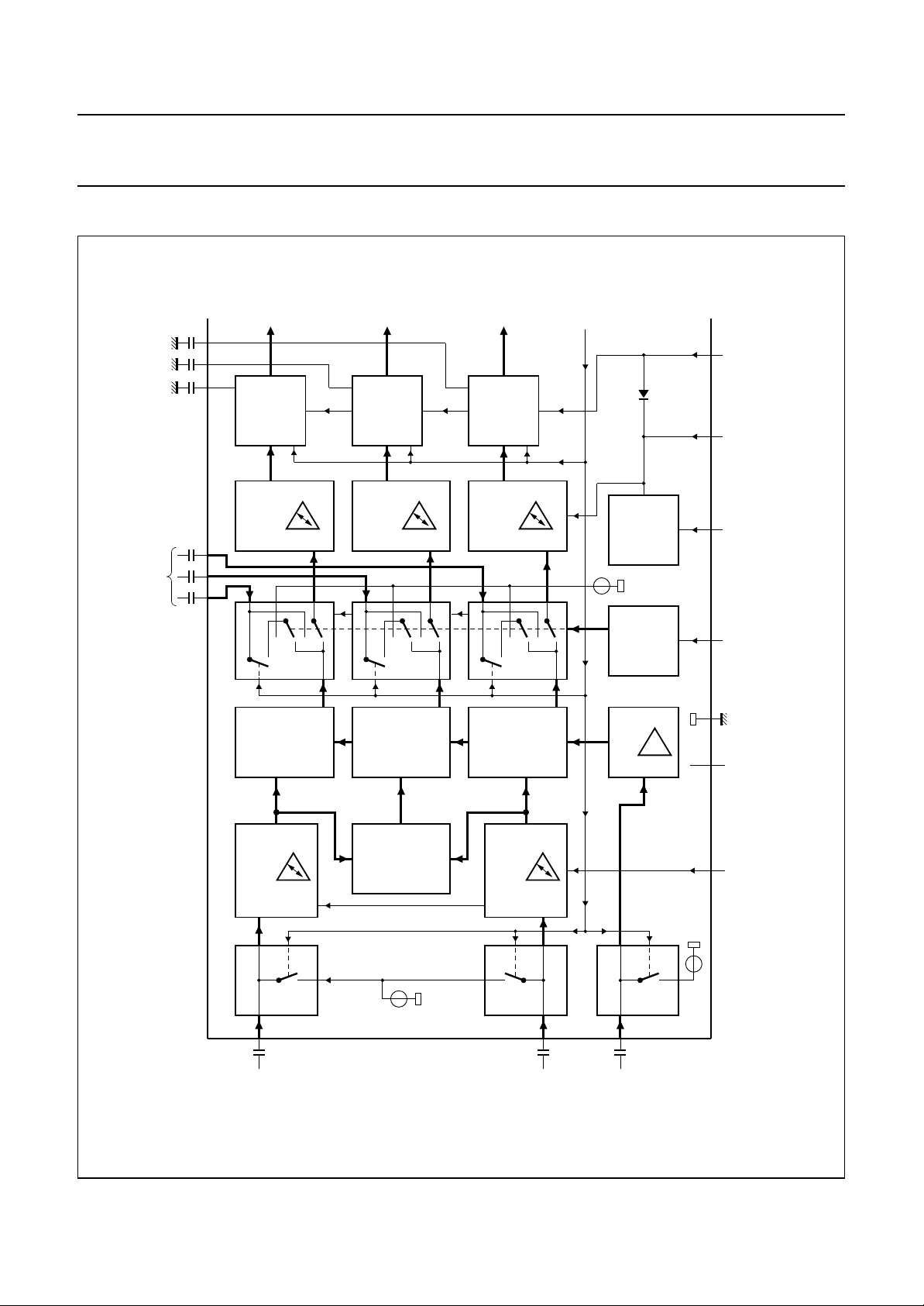
BLOCK DIAGRAM
green
CONTROL
CONTROL
BRIGHTNESS
BRIGHTNESS
CONTROL
CONTRAST
(b-w)
879
13 1214
red
CONTROL
BRIGHTNESS
CONTROL
CONTRAST
blue
CONTROL
BRIGHTNESS
CONTROL
CONTRAST
clamping pulse
4.5 V
SOURCE
CURRENT
TRESHOLD
DETECTOR
TDA3508
control
voltage
brightness
19 20
contrast control
voltage (2 to 4.3 V)
25
control input
for peak beam
current limiting
(1 to 3 V)
signal insertion 1 V
3 x SIGNAL SWITCH
R
MATRIX
(R−Y)
CONTROL
SATURATION
17 CLAMPING
11
SIGNAL
SWITCHES
DRIVER FOR
(1 V)
G
Y
(G−Y)
4.4 V
MATRIX
(G−Y)
MATRIX
Y
B
MATRIX
(B−Y)
CONTROL
SATURATION
18
CLAMPING
Y
clamping pulse
CLAMPING
15
Y
AMPLIFIER
10 dB
(part A)
TDA3508
246
16
2.9 V
input for signal
switching voltage
P
V
(+12 V)
saturation
(2 to 4.3 V)
control voltage
MSA736
handbook, full pagewidth
Fig.1 Block diagram (continued in Fig.2).
−(R−Y)
(1.05 Vp-p)
1996 Oct 25 4
−(B−Y)
(1.33 Vp-p)
composite
video
signal
(0.45 Vp-p)
Page 5
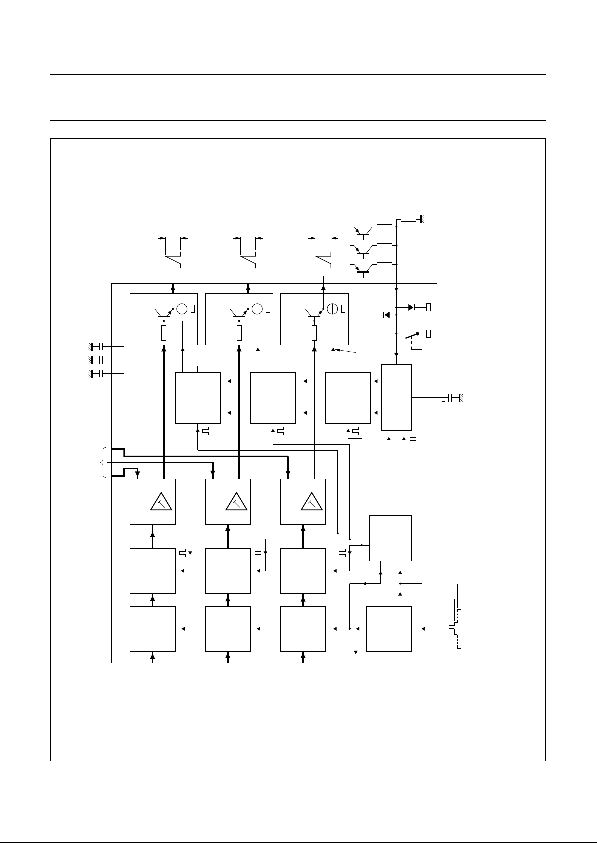
Philips Semiconductors Product specification
Video control combination circuit with
automatic cut-off control
storage capacitors
for cut-off
control
2428
red
1
CONTROLLED
OUTPUT
STAGE
2 V B/W
CONTROLLED
OUTPUT
STAGE
2 V B/W
green
3
5 blue
CONTROLLED
OUTPUT
STAGE
2 V B/W
R G B
control current
(3x)
TDA3508
MSA737
L
input for
voltage derived
from leakage
current of R
and cut-off
currents
(R or G or B)
26
+
(part B)
TDA3508
22 2123
(0 to 12 V)
white point adjustment
CONTROL
AMPLIFIER
INSERTION
PULSE
CURRENT
OF BLACK
MEASURING
BLANKING
red
&
V/I
CONVERTER
COMPARATOR
MR
CONTROL
AMPLIFIER
OF BLACK
INSERTION
PULSE
CURRENT
MEASURING
BLANKING
green
&
V/I
CONVERTER
COMPARATOR
MG
CONTROL
AMPLIFIER
OF BLACK
INSERTION
PULSE
CURRENT
MEASURING
BLANKING
blue
&
V/I
CONVERTER
COMPARATOR
MB
line 21 (1)
line 22 (1)
line 23 (1)
H + V
clamping
pulse
CIRCUIT
CLAMPING
SWITCHING AND
clamping
lines 21 to 23 (1)
lines 21 (1)
&
PULSE
FORMER
COUNTER
H + V
H
DETECTOR
SANDCASTLE
pulse
storage of leakage
current information
2.5 V
4.5 V
0
8 V
10 27
sandcastle
pulse
handbook, full pagewidth
Fig.2 Block diagram (continued from Fig.1).
1996 Oct 25 5
(1) After start of vertical blanking pulse.
Page 6

Philips Semiconductors Product specification
Video control combination circuit with
automatic cut-off control
PINNING
SYMBOL PIN DESCRIPTION
RO 1 red output
CGC 2 green storage capacitor for cut-off
control
GO 3 green output
CBC 4 blue storage capacitor for cut-off
control
BO 5 blue output
V
P
CB 7 blue storage capacitor for
CG 8 green storage capacitor for
CR 9 red storage capacitor for brightness
SC 10 sandcastle pulse input
FSW 11 fast switch for RGB inputs
BI 12 blue input (external signal)
GI 13 green input (external signal)
RI 14 red input (external signal)
Y 15 luminance input
SAT 16 saturation control input
−(R−Y) 17 colour difference input
−(B−Y) 18 colour difference input
CON 19 contrast control input
BRI 20 brightness control input
WPB 21 white point adjustment input; blue
WPG 22 white point adjustment input; green
WPR 23 white point adjustment input; red
GND 24 ground (0 V)
PBL 25 control input for peak beam current
ACO 26 automatic cut-off control input
CSL 27 storage capacitor for leakage
CRC 28 red storage capacitor for cut-off
6 supply voltage (+12 V)
brightness
brightness
limiting
current
control
handbook, halfpage
1
RO
2
CGC
3
GO
4
CBC
BO
5
V
6
P
CB
7
CG
CR
SC
FSW
BI
GI
RI
TDA3508
8
9
10
11
12
13
MSA738
Fig.3 Pin configuration.
TDA3508
CRC
28
CSL
27
ACO
26
PBL
25
GND
24
WPR
23
22
WPG
21
WPB
BRI
20
CON
19
(B Y)
18
(R Y)
17
SAT
16
1514
Y
1996 Oct 25 6
Page 7

Philips Semiconductors Product specification
Video control combination circuit with
TDA3508
automatic cut-off control
LIMITING VALUES
In accordance with the Absolute Maximum Rating System (IEC 134).
SYMBOL PARAMETER CONDITIONS MIN. MAX. UNIT
V
P
V
n
V
11
V
16,19,20
V
n1
I
1,3,5
I
19
I
20
I
25
P
tot
T
amb
T
stg
V
es
supply voltage on pin 6 0 13.2 V
input voltage on pins 10, 21, 22, 23, 25 and 26 0 V
P
V
input voltage on pin 11 −0.5 +3.0 V
input voltage on pins 16, 19 and 20 0 0.5V
voltage on pins 1 to 5, 7 to 9, 12 to 15, 17, 18,
27 and 28
no external DC voltage
V
P
V
output current on pins 1, 3 and 5 −−3mA
input current on pin 19 − 10 mA
input current on pin 20 − 5mA
input current on pin 25 −5 − mA
total power dissipation − 1.7 W
operating ambient temperature 0 70 °C
storage temperature −25 +150 °C
electrostatic handling voltage;
pin 10 note 1 −500 +450 V
all other pins note 1 −500 +500 V
Note
1. Equivalent to discharging a 200 pF capacitor via a 0 Ω series resistor.
1996 Oct 25 7
Page 8

Philips Semiconductors Product specification
Video control combination circuit with
TDA3508
automatic cut-off control
CHARACTERISTICS
V
= 12 V; V
P
12,13,14(p-p)
application circuit of Fig.4; nominal settings of brightness, contrast, saturation and white point adjustment; all voltages
referenced to ground (pin 24); unless otherwise specified.
SYMBOL PARAMETER CONDITIONS MIN. TYP. MAX. UNIT
Supply (pin 6)
V
P
I
P
supply voltage 10.8 12.0 13.2 V
supply current note 1 − 95 125 mA
Colour difference inputs (pins 17 and 18)
V
17(p-p)
−(R−Y) input signal (pin 17)
(peak-to-peak value)
V
18(p-p)
−(B−Y) input signal (pin 18)
(peak-to-peak value)
input current during scanning −−1.0 µA
I
17,18
R
I
V
17,18
input resistance 1.0 −−MΩ
internal DC voltage due to clamping note 2 3.8 4.4 4.8 V
Saturation control (pin 16)
V
16
SAT
I
16
min
input control voltages maximum saturation; note 2 4.0 4.2 4.4 V
minimum saturation V16= 1.8 V 46 50 − dB
input current −−20 µA
(G−Y) matrix (see note 3)
=1V; V
15(p-p)
= 0.45 V; V
= 1.05 V; V
17(p-p)
18(p-p)
for saturated colour bar with
75% of maximum amplitude
for saturated colour bar with
75% of maximum amplitude
nominal saturation 6 dB
below maximum; note 2
−26 dB saturation referenced
to maximum; note 2
= 1.33 V; T
=25°C; measured in
amb
− 1.05 1.48 V
− 1.33 1.88 V
2.9 3.1 3.3 V
1.9 2.1 2.3 V
Luminance input (pin 15)
V
15(p-p)
composite video input signal
− 450 630 mV
(peak-to-peak value)
input current during scanning −−1.0 µA
I
15
R
15
C
15
V
15
input resistance 0.1 −−MΩ
input capacitance −−5pF
input DC voltage due to clamping note 2 2.5 2.9 3.3 V
m linearity nominal settings 0.85 −−
RGB channels
IGNAL SWITCHING INPUT (PIN 11)
S
V
11
V
11
C
11
I
11
normal state voltage; no insertion 0 − 0.4 V
voltage level for insertion on 0.9 − 3.0 V
input capacitance −−10 pF
input current V11=0to3V −100 − +450 µA
1996 Oct 25 8
Page 9

Philips Semiconductors Product specification
Video control combination circuit with
TDA3508
automatic cut-off control
SYMBOL PARAMETER CONDITIONS MIN. TYP. MAX. UNIT
SIGNAL INSERTION: RI, GI AND BI (PINS 14, 13 AND 12)
V
14,13,12(b-w)
external RGB input signals
(black-to-white value)
I
V
input current during scanning −−1.0 µA
14,13,12
14,13,12
internal DC voltage due to clamping notes 2 and 4 4.0 4.5 5.0 V
Contrast control (pin 19)
V
19
control voltage maximum contrast; note 2 4.0 4.2 4.4 V
nominal contrast 3 dB below
maximum; note 2
−10 dB below maximum;
note 2
CON minimum contrast referenced to maximum;
=2V
V
19
I
19
RGB
diff
input current V25>6V −−2.0 µA
difference between RGB channels contrast −10 dB below
maximum
− 1.0 1.4 V
3.4 3.6 3.8 V
2.6 2.8 3.0 V
18 21 29 dB
−−0.6 dB
Peak beam current limiting (pin 25)
V
25
R
25
I
19
internal DC bias voltage note 2 5.3 5.5 5.7 V
input resistance − 10 − kΩ
input current at contrast control
input
Brightness control (pin 20)
V
I
20
∆V
20
blk(b-w)
control voltage note 2 1.0 − 3.0 V
input current no beam current limiting −−−10 µA
shift of black level in the control
range referenced to the luminance
signal (black-to-white value)
tracking 95 −−%
Internal signal limiting (RGB)
signal limiting referenced to nominal
luminance and nominal black level
White point adjustment (pins 21, 22 and 23); note 2
G
v
R
I
AC voltage gain V
input resistance − 20 − kΩ
V25= 4.5 V 10 20 34 mA
∆V20=1V −±50 − %
black −−25 − %
white 115 120 125 %
21,22,23
V
21,22,23
V
21,22,23
= 5.5 V; note 5 − 100 − %
= 0 V; note 5 −35 −40 − %
= 12 V; note 5 +35 +40 − %
1996 Oct 25 9
Page 10

Philips Semiconductors Product specification
Video control combination circuit with
TDA3508
automatic cut-off control
SYMBOL PARAMETER CONDITIONS MIN. TYP. MAX. UNIT
RGB outputs (emitter follower; pins 1, 3 and 5)
V
1,3,5
V
1,3,5
∆V
1,3,5
V
1,3,5
I
internal current source 2.0 3.0 − mA
1,3,5
Automatic cut-off control (pin 26); notes 2, 6, 7, 8 and 9
V
26
V
26
Gain data (at nominal brightness, contrast, saturation and white point settings)
G
v1,3,5-15
α
1,3,5-15
G
v
α frequency response of colour
G
v
α frequency response of inserted
t
r
t
f
∆t
1,3,5
t
d
∆G
v1,3,5
output voltage black-to-white positive 1.5 2.0 2.5 V
black level without automatic cut-off
V
= 10 V; note 2 6.1 6.9 7.7 V
28,2,4
control
difference in black level between
−−10 mV
RGB channels due to variation of
contrast control
cut-off control range note 2 4.0 4.6 − V
input voltage 0 − 6.5 V
voltage difference between cut-off
0.5 0.64 0.72 V
current measurement and leakage
current measurement
voltage gain with respect to
14 16 18 dB
luminance input (pin 15)
frequency response of luminance
fi=0to5MHz −−3dB
path
voltage gain with respect to colour
369dB
difference inputs
(pins 1 to 17 and 5 to 18)
f
=0to2MHz −−3dB
i
difference paths
(pins 1 to 17 and 5 to 18)
voltage gain with respect to inserted
468dB
signals (pins 1 to 14, 3 to 13
and 5 to 12)
f
=0to10MHz −−3dB
i
signal paths (pins 1 to 14, 3 to 13
and 5 to 12)
rise time of RGB output signals
− 40 − ns
(pins 1, 3 and 5)
fall time of RGB output signals
− 40 − ns
(pins 1, 3 and 5)
difference in transition times
− 015ns
between R, G and B channels
delay time between signal switching
−25 − +25 ns
and signal insertion
difference in gain between normal
−−10 %
and signal insertion mode
1996 Oct 25 10
Page 11

Philips Semiconductors Product specification
Video control combination circuit with
TDA3508
automatic cut-off control
SYMBOL PARAMETER CONDITIONS MIN. TYP. MAX. UNIT
Sandcastle pulse detector (pin 10)
V
10
the following amplitudes are
required for separating the various
pulses
I
10
input current −−−110 µA
Notes
1. Maximum value <110 mA after warm-up.
2. Values are proportional to the supply voltage.
3. Matrixed according to equation V
4. When V
< 0.4 V during clamping time, the black levels of the inserted RGB signals are clamped on the black
11-24
levels of the internal RGB signals. When V
(G−Y)
= −0.51V
11-24
signals are clamped on an internal DC voltage (correct clamping of the external RGB signals is possible only when
they are synchronous with the sandcastle pulse).
5. When pins 21, 22 and 23 are not connected, an internal bias voltage of 5.5 V is supplied.
6. Automatic cut-off control measurement occurs in the following lines after start of the vertical blanking pulse:
a) line 20: measurement of leakage current (R + G + B).
b) line 21: measurement of red cut-off current.
c) line 22: measurement of green cut-off current.
d) line 23: measurement of blue cut-off current.
7. Black level of the measured channel is nominal; the other two channels are blanked to ultra-black.
8. All three channels blanked to ultra-black. The cut-off control cycle occurs when the vertical blanking part of the
sandcastle pulse contains more than 3 line pulses. The internal blanking continues until the end of the last measured
line. The vertical blanking pulse is not allowed to contain more than 34 line pulses, otherwise another control cycle
begins.
9. Input pin 26 switches to ground during horizontal flyback.
10. The sandcastle pulse is compared with three internal thresholds (proportional to VP) and the given levels separate
the various pulses.
11. Blanked to ultra-black (−25%).
12. Pulse duration ≥3.5 µs.
horizontal and vertical
1.0 1.5 2.0 V
blanking; notes 10 and 11
required pulses (H + V);
2.1 2.5 2.9 V
note 10
horizontal; note 10 3.0 3.5 4.0 V
required pulses (H); note 10 4.1 4.5 5.0 V
clamping; notes 10 and 12 6.5 7.0 7.5 V
required pulses; note 10 7.6 − 12.0 V
no keying; note 10 −−1.0 V
(R−Y)
− 0.19V
(B−Y)
.
> 0.9 V during clamping time, the black levels of the inserted RGB
1996 Oct 25 11
Page 12

Philips Semiconductors Product specification
Video control combination circuit with
automatic cut-off control
APPLICATION INFORMATION
22 µH
+200 V
+12 V
10
pF
(2)
B
22 µF
100
kΩ
1.6
kΩ
1.5
kΩ
BC558
sandcastle
pulse
signal switch
pulse
signal
insertion
18 kΩ
1N4148
22 pF
1N4148
BF869
+12 V
(VP)
(1) When supplied via a 75 Ω line.
(2) Capacitor value depends on circuit layout.
−B
560 Ω 820 Ω 18 kΩ 560 Ω 820 Ω 18 kΩ 560 Ω 820 Ω
BF869
1N4148
22 µH
22 µF
1 V
B 1 V (b-w)
G 1 V (b-w)
R 1 V (b-w)
BF423
33
kΩ
10
(2)
pF
GR
+12 V
(to other circuitry)
75 Ω
75 Ω
75 Ω
75 Ω
100kΩ1.5
BC558
1.6
kΩ
180 Ω
330 nF
180 Ω
330 nF
180 Ω
22 nF
22 nF
22 nF
22 nF
(1)
22 nF
(1)
22 nF
(1)
(1)
kΩ
(2)
−G −R
BF869
1N4148
1N4148
(2)
22 pF
BF869 BF869
1
2
3
4
5
6
7
BF423
33
kΩ
100
kΩ
1.6
10
(2)
kΩ
pF
28
330 nF
27
26
25
24
23
22
1N4148
22 pF
1.5
kΩ
BC558
1N4148
22 µF
RGB
10
kΩ
TDA3508
8
9
10
11
12
13
14
+12 V
8.2 kΩ
3.9 kΩ
21
20
19
18
17
16
15
100 nF
1N4148
1N4148
22 nF
4.7
µF
240 kΩ
22 nF
22 µF
5.6
kΩ
180 kΩ
15 kΩ
910 kΩ
22 kΩ
1
kΩ
BF869
1N4148
(2)
dark current
100 pF
56 kΩ
1N4148
1.5 kΩ
1N4148
10
kΩ
100 kΩ
Y
delay line
BF423
33
kΩ
BC558
100 nF
56 kΩ
680 kΩ
22 nF
22 nF
56 kΩ
1 kΩ
10 kΩ
MSA735
10
kΩ
TDA3508
560
680
Ω
Ω
560
1 nF
Ω
+12 V
peak beam current
limiting (actual value)
+12 V
brightness
0 to 12 V
contrast
0 to 12 V
−(B−Y)
1.33 V (p-p)
−(R−Y)
1.05 V (p-p)
saturation
0 to 12 V
Y
(1 V composite
video signal)
beam current
(actual value)
Fig.4 Typical application circuit diagram using TDA3508; colour difference inputs are negative.
1996 Oct 25 12
Page 13

Philips Semiconductors Product specification
Video control combination circuit with
automatic cut-off control
PACKAGE OUTLINE
handbook, full pagewidth
DIP28: plastic dual in-line package; 28 leads (600 mil)
D
seating plane
L
Z
28
e
b
TDA3508
SOT117-1
M
E
A
2
A
A
1
w M
b
1
15
c
(e )
1
M
H
pin 1 index
1
0 5 10 mm
scale
DIMENSIONS (inch dimensions are derived from the original mm dimensions)
A
A
A
UNIT
inches
Note
1. Plastic or metal protrusions of 0.25 mm maximum per side are not included.
max.
mm
1 2
min.
max.
b
1.7
1.3
0.066
0.051
b
0.53
0.38
0.020
0.014
cD E weM
1
0.32
0.23
0.013
0.009
(1) (1)
36.0
35.0
1.41
1.34
14.1
13.7
0.56
0.54
E
14
(1)
L
3.9
3.4
M
E
15.80
15.24
0.62
0.60
H
17.15
15.90
0.68
0.63
0.252.54 15.24
0.010.10 0.60
e
1
0.15
0.13
Z
max.
1.75.1 0.51 4.0
0.0670.20 0.020 0.16
OUTLINE
VERSION
SOT117-1
IEC JEDEC EIAJ
051G05 MO-015AH
REFERENCES
1996 Oct 25 13
EUROPEAN
PROJECTION
ISSUE DATE
92-11-17
95-01-14
Page 14

Philips Semiconductors Product specification
Video control combination circuit with
automatic cut-off control
SOLDERING
Introduction
There is no soldering method that is ideal for all IC
packages. Wave soldering is often preferred when
through-hole and surface mounted components are mixed
on one printed-circuit board. However, wave soldering is
not always suitable for surface mounted ICs, or for
printed-circuits with high population densities. In these
situations reflow soldering is often used.
This text gives a very brief insight to a complex technology.
A more in-depth account of soldering ICs can be found in
our
“IC Package Databook”
Soldering by dipping or by wave
The maximum permissible temperature of the solder is
260 °C; solder at this temperature must not be in contact
with the joint for more than 5 seconds. The total contact
time of successive solder waves must not exceed
5 seconds.
(order code 9398 652 90011).
TDA3508
The device may be mounted up to the seating plane, but
the temperature of the plastic body must not exceed the
specified maximum storage temperature (T
printed-circuit board has been pre-heated, forced cooling
may be necessary immediately after soldering to keep the
temperature within the permissible limit.
Repairing soldered joints
Apply a low voltage soldering iron (less than 24 V) to the
lead(s) of the package, below the seating plane or not
more than 2 mm above it. If the temperature of the
soldering iron bit is less than 300 °C it may remain in
contact for up to 10 seconds. If the bit temperature is
between 300 and 400 °C, contact may be up to 5 seconds.
stg max
). If the
DEFINITIONS
Data sheet status
Objective specification This data sheet contains target or goal specifications for product development.
Preliminary specification This data sheet contains preliminary data; supplementary data may be published later.
Product specification This data sheet contains final product specifications.
Limiting values
Limiting values given are in accordance with the Absolute Maximum Rating System (IEC 134). Stress above one or
more of the limiting values may cause permanent damage to the device. These are stress ratings only and operation
of the device at these or at any other conditions above those given in the Characteristics sections of the specification
is not implied. Exposure to limiting values for extended periods may affect device reliability.
Application information
Where application information is given, it is advisory and does not form part of the specification.
LIFE SUPPORT APPLICATIONS
These products are not designed for use in life support appliances, devices, or systems where malfunction of these
products can reasonably be expected to result in personal injury. Philips customers using or selling these products for
use in such applications do so at their own risk and agree to fully indemnify Philips for any damages resulting from such
improper use or sale.
1996 Oct 25 14
Page 15

Philips Semiconductors Product specification
Video control combination circuit with
automatic cut-off control
NOTES
TDA3508
1996 Oct 25 15
Page 16

Philips Semiconductors – a worldwide company
Argentina: see South America
Australia: 34 Waterloo Road, NORTH RYDE, NSW 2113,
Tel. +61 2 9805 4455, Fax. +61 2 9805 4466
Austria: Computerstr. 6, A-1101 WIEN, P.O. Box 213,
Tel. +43 1 60 101, Fax. +43 1 60 101 1210
Belarus: Hotel Minsk Business Center, Bld. 3, r. 1211, Volodarski Str. 6,
220050 MINSK, Tel. +375 172 200 733, Fax. +375 172 200 773
Belgium: see The Netherlands
Brazil: see South America
Bulgaria: Philips Bulgaria Ltd., Energoproject, 15th floor,
51 James Bourchier Blvd., 1407 SOFIA,
Tel. +359 2 689 211, Fax. +359 2 689 102
Canada: PHILIPS SEMICONDUCTORS/COMPONENTS,
Tel. +1 800 234 7381
China/Hong Kong: 501 Hong Kong Industrial Technology Centre,
72 Tat Chee Avenue, Kowloon Tong, HONG KONG,
Tel. +852 2319 7888, Fax. +852 2319 7700
Colombia: see South America
Czech Republic: see Austria
Denmark: Prags Boulevard 80, PB 1919, DK-2300 COPENHAGEN S,
Tel. +45 32 88 2636, Fax. +45 31 57 1949
Finland: Sinikalliontie 3, FIN-02630 ESPOO,
Tel. +358 9 615800, Fax. +358 9 61580/xxx
France: 4 Rue du Port-aux-Vins, BP317, 92156 SURESNES Cedex,
Tel. +33 1 40 99 6161, Fax. +33 1 40 99 6427
Germany: Hammerbrookstraße 69, D-20097 HAMBURG,
Tel. +49 40 23 53 60, Fax. +49 40 23 536 300
Greece: No. 15, 25th March Street, GR 17778 TAVROS/ATHENS,
Tel. +30 1 4894 339/239, Fax. +30 1 4814 240
Hungary: see Austria
India: Philips INDIA Ltd, Shivsagar Estate, A Block, Dr. Annie Besant Rd.
Worli, MUMBAI 400 018, Tel. +91 22 4938 541, Fax. +91 22 4938 722
Indonesia: see Singapore
Ireland: Newstead, Clonskeagh, DUBLIN 14,
Tel. +353 1 7640 000, Fax. +353 1 7640 200
Israel: RAPAC Electronics, 7 Kehilat Saloniki St, TEL AVIV 61180,
Tel. +972 3 645 0444, Fax. +972 3 649 1007
Italy: PHILIPS SEMICONDUCTORS, Piazza IV Novembre 3,
20124 MILANO, Tel. +39 2 6752 2531, Fax. +39 2 6752 2557
Japan: Philips Bldg 13-37, Kohnan 2-chome, Minato-ku, TOKYO 108,
Tel. +81 3 3740 5130, Fax. +81 3 3740 5077
Korea: Philips House, 260-199 Itaewon-dong, Yongsan-ku, SEOUL,
Tel. +82 2 709 1412, Fax. +82 2 709 1415
Malaysia: No. 76 Jalan Universiti, 46200 PETALING JAYA, SELANGOR,
Tel. +60 3 750 5214, Fax. +60 3 757 4880
Mexico: 5900 Gateway East, Suite 200, EL PASO, TEXAS 79905,
Tel. +9-5 800 234 7381
Middle East: see Italy
Netherlands: Postbus 90050, 5600PB EINDHOVEN, Bldg. VB,
Tel. +3140 27 82785, Fax. +31 40 27 88399
New Zealand: 2 Wagener Place, C.P.O. Box 1041, AUCKLAND,
Tel. +64 9 849 4160, Fax. +64 9 849 7811
Norway: Box 1, Manglerud 0612, OSLO,
Tel. +47 22 74 8000, Fax. +47 22 74 8341
Philippines: Philips Semiconductors Philippines Inc.,
106 Valero St. Salcedo Village, P.O. Box 2108 MCC, MAKATI,
Metro MANILA, Tel. +63 2 816 6380, Fax. +63 2 817 3474
Poland: Ul. Lukiska 10, PL 04-123 WARSZAWA,
Tel. +48 22 612 2831, Fax. +48 22 612 2327
Portugal: see Spain
Romania: see Italy
Russia: Philips Russia, Ul. Usatcheva 35A, 119048 MOSCOW,
Tel. +7 095 247 9145, Fax. +7 095 247 9144
Singapore: Lorong 1, Toa Payoh, SINGAPORE 1231,
Tel. +65 350 2538, Fax. +65 251 6500
Slovakia: see Austria
Slovenia: see Italy
South Africa: S.A. PHILIPS Pty Ltd., 195-215 Main Road Martindale,
2092 JOHANNESBURG, P.O. Box 7430 Johannesburg 2000,
Tel. +27 11 470 5911, Fax. +27 11 470 5494
South America: Rua do Rocio 220, 5th floor, Suite 51,
04552-903 São Paulo, SÃO PAULO - SP, Brazil,
Tel. +55 11 821 2333, Fax. +55 11 829 1849
Spain: Balmes 22, 08007 BARCELONA,
Tel. +34 3 301 6312, Fax. +34 3 301 4107
Sweden: Kottbygatan 7, Akalla, S-16485 STOCKHOLM,
Tel. +46 8 632 2000, Fax. +46 8 632 2745
Switzerland: Allmendstrasse 140, CH-8027 ZÜRICH,
Tel. +41 1 488 2686, Fax. +41 1 481 7730
Taiwan: PHILIPS TAIWAN Ltd., 23-30F, 66,
Chung Hsiao West Road, Sec. 1, P.O. Box 22978,
TAIPEI 100, Tel. +886 2 382 4443, Fax. +886 2 382 4444
Thailand: PHILIPS ELECTRONICS (THAILAND) Ltd.,
209/2 Sanpavuth-Bangna Road Prakanong, BANGKOK 10260,
Tel. +66 2 745 4090, Fax. +66 2 398 0793
Turkey: Talatpasa Cad. No. 5, 80640 GÜLTEPE/ISTANBUL,
Tel. +90 212 279 2770, Fax. +90 212 282 6707
Ukraine: PHILIPS UKRAINE, 4 Patrice Lumumba str., Building B, Floor 7,
252042 KIEV, Tel. +380 44 264 2776, Fax. +380 44 268 0461
United Kingdom: Philips Semiconductors Ltd., 276 Bath Road, Hayes,
MIDDLESEX UB3 5BX, Tel. +44 181 730 5000, Fax. +44 181 754 8421
United States: 811 East Arques Avenue, SUNNYVALE, CA 94088-3409,
Tel. +1 800 234 7381
Uruguay: see South America
Vietnam: see Singapore
Yugoslavia: PHILIPS, Trg N. Pasica 5/v, 11000 BEOGRAD,
Tel. +381 11 625 344, Fax.+381 11 635 777
For all other countries apply to: Philips Semiconductors, Marketing & Sales Communications,
Building BE-p, P.O. Box 218, 5600 MD EINDHOVEN, The Netherlands, Fax. +31 40 27 24825
© Philips Electronics N.V. 1996 SCA52
All rights are reserved. Reproduction in whole or in part is prohibited without the prior written consent of the copyright owner.
The information presented in this document does not form part of any quotation or contract, is believed to be accurate and reliable and may be changed
without notice. No liability will be accepted by the publisher for any consequence of its use. Publication thereof does not convey nor imply any license
under patent- or other industrial or intellectual property rights.
Internet: http://www.semiconductors.philips.com
Printed in The Netherlands 537021/1200/02/pp16 Date of release: 1996 Oct 25 Document order number: 9397 750 00968
 Loading...