

Page 1

DATA SH EET
Product specification
Supersedes data of July 1994
File under Integrated Circuits, IC01
1995 May 08
INTEGRATED CIRCUITS
Philips Semiconductors
TDA2615
2 × 6 W hi-fi audio power amplifier
Page 2

1995 May 08 2
Philips Semiconductors Product specification
2 × 6 W hi-fi audio power amplifier TDA2615
FEATURES
• Requires very few external components
• No switch-on/switch-off clicks
• Input mute during switch-on and switch-off
• Low offset voltage between output and ground
• Excellent gain balance of both amplifiers
• Hi-fi in accordance with
“IEC 268”
and
“DIN 45500”
• Short-circuit proof and thermal protected
• Mute possibility.
GENERAL DESCRIPTION
The TDA2615 is a dual power amplifier in a 9-lead plastic
single-in-line (SIL9MPF) medium power package. It has
been especially designed for mains fed applications, such
as stereo radio and stereo TV.
QUICK REFERENCE DATA
Stereo application.
ORDERING INFORMATION
SYMBOL PARAMETER CONDITIONS MIN. TYP. MAX. UNIT
±V
P
supply voltage range 7.5 − 21 V
P
O
output power VS= ±12 V; THD = 0.5% − 6 − W
G
v
internal voltage gain − 30 − dB
G
v
channel unbalance − 0.2 − dB
α channel separation − 70 − dB
SVRR supply voltage ripple rejection − 60 − dB
V
no
noise output voltage − 70 −µV
TYPE
NUMBER
PACKAGE
NAME DESCRIPTION VERSION
TDA2615 SIL9MPF
plastic single in-line medium power package with fin; 9 leads
SOT110-1
Page 3
1995 May 08 3
Philips Semiconductors Product specification
2 × 6 W hi-fi audio power amplifier TDA2615
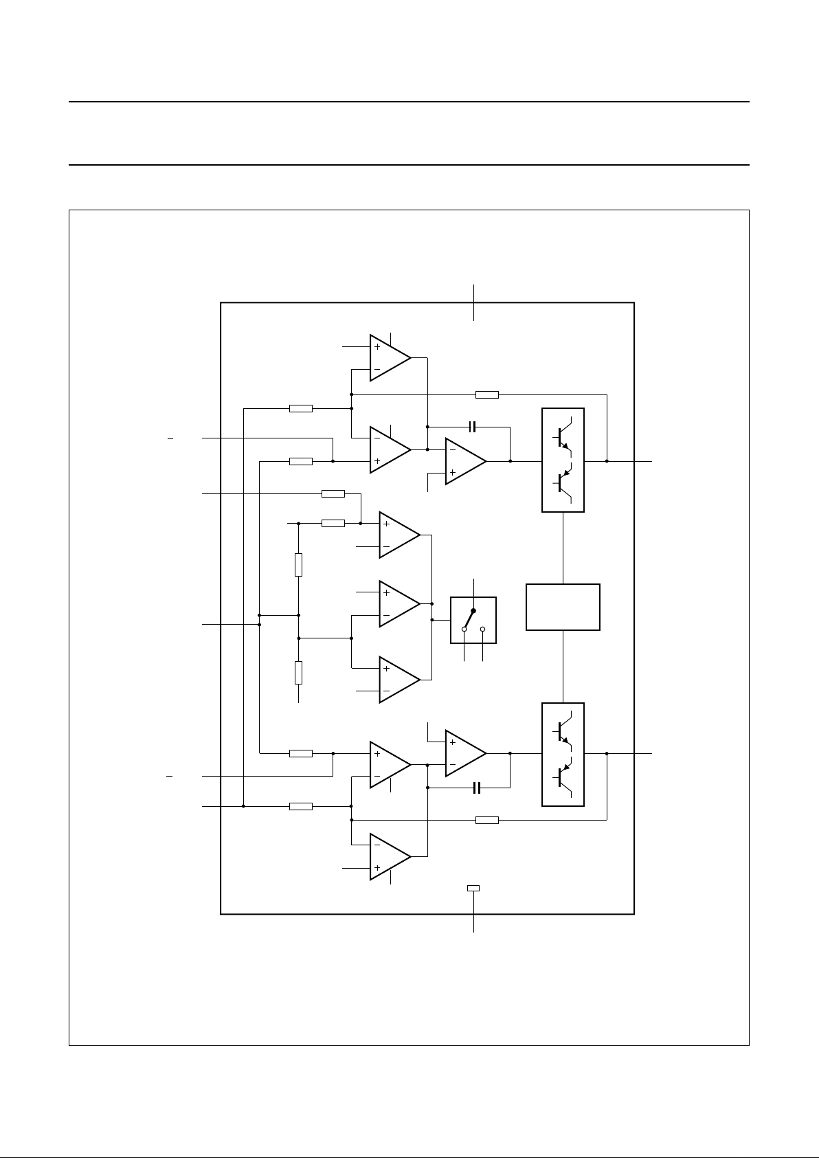
BLOCK DIAGRAM
Fig.1 Block diagram.
MLA711
5
voltage
comparator
4
4 kΩ
10 kΩ
P
– V
P
+ V
THERMAL
PROTECTION
5 kΩ
1
CM
20 kΩ
V
A
B
V
P
– V
680 Ω
20 kΩ
10 kΩ
V
A
B
V
P
+ V
ref1
V
ref3
V
ref2
+ V
ref2
– V
P
+ V
CM
20 kΩ
V
A
B
V
P
– V
680 Ω
20 kΩ
ref1
V
ref1
V
6
P
– V
8
9
3
2
TDA2615
INV1
MUTE
1/2 V / GND
OUT1
OUT2
INV1, 2
INV2
P
7
Page 4
1995 May 08 4
Philips Semiconductors Product specification
2 × 6 W hi-fi audio power amplifier TDA2615
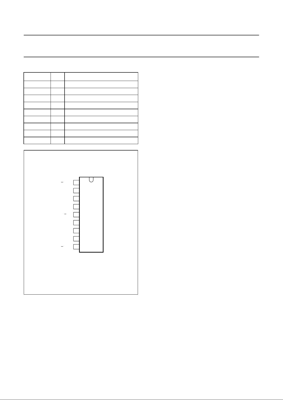
PINNING
SYMBOL PIN DESCRIPTION
−INV1 1 non-inverting input 1
MUTE 2 mute input
1
⁄2VP/GND 31⁄2 supply voltage or ground
OUT1 4 output 1
−V
P
5 supply voltage (negative)
OUT2 6 output 2
+V
P
7 supply voltage (positive)
INV1, 2 8 inverting input 1 and 2
−INV2 9 non-inverting input 2
Fig.2 Pin configuration.
MLA708
1
2
3
4
5
6
7
8
9
P
+ V
OUT2
MUTE
INV2
TDA2615
/ GND
P
V
INV1
INV1, 2
OUT1
1/2 V
P
FUNCTIONAL DESCRIPTION
The TDA2615 is a hi-fi stereo amplifier designed for mains
fed applications, such as stereo radio and stereo TV. The
circuit is optimally designed for symmetrical power
supplies, but is also well-suited to asymmetrical power
supply systems.
An output power of 2 × 6W (THD = 0.5%) can be
delivered into an 8 Ω load with a symmetrical power supply
of ±12 V. The gain is internally fixed at 30 dB, thus offering
a low gain spread and a very good gain balance between
the two amplifiers (0.2 dB).
A special feature is the input mute circuit. This circuit
disconnects the non-inverting inputs when the supply
voltage drops below±6 V, while the amplifier still retains its
DC operating adjustment. The circuit features suppression
of unwanted signals at the inputs, during switch-on and
switch-off.
The mute circuit can also be activated via pin 2. When a
current of 300 µA is present at pin 2, the circuit is in the
mute condition.
The device is provided with two thermal protection circuits.
One circuit measures the average temperature of the
crystal and the other measures the momentary
temperature of the power transistors. These control
circuits attack at temperatures in excess of +150 °C, so a
crystal operating temperature of max. +150 °C can be
used without extra distortion.
With the derating value of 6 K/W, the heatsink can be
calculated as follows:
at R
L
=8Ω and VS= ±12 V, the measured maximum
dissipation is 7.8 W.
With a maximum ambient temperature of +60 °C, the
thermal resistance of the heatsink is:
The metal tab has the same potential as pin 5.
R
th
150 60–
7.8
----------------------
6– 5.5 K/W==
Page 5

1995 May 08 5
Philips Semiconductors Product specification
2 × 6 W hi-fi audio power amplifier TDA2615
LIMITING VALUES
In accordance with the Absolute maximum System (IEC 134).
Note
1. For asymmetrical power supplies (with the load short-circuited), the maximum unloaded supply voltage is limited to
V
P
= 28 V and with an internal supply resistance of RS≥ 4 Ω, the maximum unloaded supply voltage is limited to 32 V
(with the load short-circuited). For symmetrical power supplies the circuit is short-circuit-proof up to VP=21V.
SYMBOL PARAMETER CONDITIONS MIN. MAX. UNIT
±V
P
supply voltage − 21 V
I
OSM
non-repetitive peak output current − 4A
P
tot
total power dissipation see Fig.3 − 15 W
T
stg
storage temperature range −55 +150 °C
T
xtal
crystal temperature − +150 °C
T
amb
ambient operating temperature range −25 +150 °C
t
sc
short-circuit time short-circuit to ground; note 1 − 1h
Fig.3 Power derating curve.
– 25 0 50 150
16
12
4
0
8
MCD368 - 2
100
T ( C)
o
amb
P
(W)
tot
infinite heatsink
R = 5.5 K/W
th-hs
THERMAL CHARACTERISTICS
SYMBOL PARAMETER VALUE UNIT
R
th j-c
thermal resistance from junction to case 6 K/W
Page 6

1995 May 08 6
Philips Semiconductors Product specification
2 × 6 W hi-fi audio power amplifier TDA2615
CHARACTERISTICS
SYMBOL PARAMETER CONDITIONS MIN. TYP. MAX. UNIT
Supply
±V
P
supply voltage range − 12 21 V
I
ORM
repetitive peak output current 2.2 −−A
Operating position; note 1
±V
P
supply voltage range 7.5 12 21 V
I
q(tot)
total quiescent current RL= ∞ 18 40 70 mA
P
O
output power THD = 0.5% 5 6 − W
THD = 10% 6.5 8 − W
THD total harmonic distortion PO=4W − 0.15 0.2 %
B power bandwidth THD = 0.5%; note 2 − 20 to 20000 − Hz
G
v
voltage gain 29 30 31 dB
G
v
gain unbalance − 0.2 1 dB
V
no
noise output voltage note 3 − 70 140 µV
Z
i
input impedance 14 20 26 kΩ
SVRR supply voltage ripple rejection note 4 40 60 − dB
α
cs
channel separation RS= 0 46 70 − dB
I
bias
input bias current − 0.3 −µA
∆V
GND
DC output offset voltage − 30 200 mV
∆V
4−6
DC output offset voltage between two channels − 4 150 mV
MUTE POSITION (AT I
MUTE
≥ 300 µA)
V
O
output voltage VI= 600 mV − 0.3 1.0 mV
Z
2−7
mute input impedance − 9 − kΩ
I
q(tot)
total quiescent current RL= ∞ 18 40 70 mA
V
no
noise output voltage note 3 − 70 140 µV
SVRR supply voltage ripple rejection note 4 40 55 − dB
∆V
GND
DC output offset voltage − 40 200 mV
∆V
off
offset voltage with respect to
operating position
− 4 150 mV
I
2
current if pin 2 is connected to pin 5 −− 6mA
Mute position; note 5
±V
P
supply voltage range 2 − 5.8 V
I
P
total quiescent current RL= ∞ 930 40mA
V
O
output voltage VI= 600 mV − 0.3 1.0 mV
V
no
noise output voltage note 3 − 70 140 µV
SVRR supply voltage ripple rejection note 4 40 55 − dB
∆V
GND
DC output offset voltage − 40 200 mV
Page 7

1995 May 08 7
Philips Semiconductors Product specification
2 × 6 W hi-fi audio power amplifier TDA2615
Notes
1. VP= ±12 V; RL=8Ω; T
amb
=25°C; fi= 1 kHz; symmetrical power supply I
MUTE
= < 30 µA (see Fig.4).
2. The power bandwidth is measured at a maximum output power (P
Omax
) of −3 dB.
3. The noise output voltage (RMS value) is measured at RS=2kΩ, unweighted (20 Hz to 20 kHz).
4. The ripple rejection is measured at RS= 0 and fi= 100 Hz to 20 kHz. The ripple voltage (200 mV) is applied in phase
to the positive and the negative supply rails. With asymmetrical power supplies, the ripple rejection is measured at
fi= 1 kHz.
5. ±VP= 4 V; RL=8Ω; T
amb
=25°C; fi= 1 kHz; symmetrical power supply (see Fig.4).
6. VP= 24 V; RL=8Ω; T
amb
=25°C; fi= 1 kHz; asymmetrical power supply I
MUTE
< 30 µA (see Fig.5).
7. The internal network at pin 2 is a resistor divider of typical 4 kΩ and 5 kΩ to the positive supply rail. At the connection
of the 4 kΩ and 5 kΩ resistor a zener diode of typical 6.6 V is also connected to the positive supply rail. The spread
of the zener voltage is 6.1 to 7.1 V.
Operating position; note 6
I
q(tot)
total quiescent current 18 40 70 mA
P
O
output power THD = 0.5% 5 6 − W
THD = 10% 6.5 8 − W
THD total harmonic distortion P
O
=4W − 0.13 0.2 %
B power bandwidth THD = 0.5%; note 1 − 40 to 20000 − Hz
G
v
voltage gain 29 30 31 dB
G
v
gain unbalance − 0.2 1 dB
V
no
noise output voltage note 3 − 70 140 µV
Z
i
input impedance 14 20 26 kΩ
SVRR supply voltage ripple rejection 35 44 − dB
α
cs
channel separation − 45 − dB
MUTE POSITION (I
MUTE
≥ 300 µA)
V
O
output voltage VI= 600 mV − 0.3 1.0 mV
Z
2−7
mute input impedance note 7 6.7 9 11.3 kΩ
I
q(tot)
total quiescent current 18 40 70 mA
V
no
noise output voltage note 3 − 70 140 µV
SVRR supply voltage ripple rejection note 4 35 44 − dB
∆V
off
offset voltage with respect to operating
position
− 4 150 mV
I
2
current if pin 2 is connected to pin 5 −− 6mA
SYMBOL PARAMETER CONDITIONS MIN. TYP. MAX. UNIT
Page 8

1995 May 08 8
Philips Semiconductors Product specification
2 × 6 W hi-fi audio power amplifier TDA2615
TEST AND APPLICATION INFORMATION
Fig.4 Test and application circuit with symmetrical power supply.
2200 µF
72
mute input
P
+ V
5
TDA2615
MLA710 - 2
100 nF
6
20 kΩ
8
20 kΩ680 Ω
220 nF
9
R = 8 Ω
L
22 nF
8.2 Ω
I
V
P
– V
3
R = 8 Ω
L
22 nF
8.2 Ω
4
20 kΩ
220 nF
1
I
V
20 kΩ680 Ω
2200 µF
Page 9

1995 May 08 9
Philips Semiconductors Product specification
2 × 6 W hi-fi audio power amplifier TDA2615
Fig.5 Test and application circuit with asymmetrical power supply.
6
20 kΩ
5
8
3
MLA709 - 1
20 kΩ680 Ω
9
R = 8 Ω
L
22 nF
680 µF
8.2 Ω
100 nF
2200 µF
72
mute input
S
V
S
R
P
V
2
4
20 kΩ
1
220 nF
100 µF
I
V
220 nF
I
V
20 kΩ680 Ω
P
1/2 V
internal
R = 8 Ω
L
22 nF
680 µF
8.2 Ω
TDA2615
Page 10

1995 May 08 10
Philips Semiconductors Product specification
2 × 6 W hi-fi audio power amplifier TDA2615
PACKAGE OUTLINE
UNIT
A
A
max.
2
A
3
b
1
D
1
b
2
bcD
(1)
E
(1)
Z
max.
(1)
eLPP
1
q1q
2
q
REFERENCES
OUTLINE
VERSION
EUROPEAN
PROJECTION
ISSUE DATE
IEC JEDEC EIAJ
mm
18.5
17.8
3.7
8.7
8.0
A
4
15.8
15.4
1.40
1.14
0.67
0.50
1.40
1.14
0.48
0.38
21.8
21.4
21.4
20.7
6.48
6.20
3.4
3.2
2.54
1.0
5.9
5.7
4.4
4.2
3.9
3.4
15.1
14.9
Q
1.75
1.55
DIMENSIONS (mm are the original dimensions)
Note
1. Plastic or metal protrusions of 0.25 mm maximum per side are not included.
2.75
2.50
SOT110-1
92-11-17
95-02-25
0 5 10 mm
scale
0.25
w
D
E
A
A
c
A
2
3
A
4
q
1
q
2
L
Q
w M
b
b
1
b
2
D
1
P
q
1
Z
e
19
P
seating plane
pin 1 index
SIL9MPF: plastic single in-line medium power package with fin; 9 leads
SOT110-1
Page 11

1995 May 08 11
Philips Semiconductors Product specification
2 × 6 W hi-fi audio power amplifier TDA2615
SOLDERING
Plastic single in-line packages
B
Y DIP OR WAVE
The maximum permissible temperature of the solder is
260 °C; this temperature must not be in contact with the
joint for more than 5 s. The total contact time of successive
solder waves must not exceed 5 s.
The device may be mounted up to the seating plane, but
the temperature of the plastic body must not exceed the
specified storage maximum. If the printed-circuit board has
been pre-heated, forced cooling may be necessary
immediately after soldering to keep the temperature within
the permissible limit.
R
EPAIRING SOLDERED JOINTS
Apply the soldering iron below the seating plane (or not
more than 2 mm above it). If its temperature is below
300 °C, it must not be in contact for more than 10 s; if
between 300 and 400 °C, for not more than 5 s.
DEFINITIONS
LIFE SUPPORT APPLICATIONS
These products are not designed for use in life support appliances, devices, or systems where malfunction of these
products can reasonably be expected to result in personal injury. Philips customers using or selling these products for
use in such applications do so at their own risk and agree to fully indemnify Philips for any damages resulting from such
improper use or sale.
Data sheet status
Objective specification This data sheet contains target or goal specifications for product development.
Preliminary specification This data sheet contains preliminary data; supplementary data may be published later.
Product specification This data sheet contains final product specifications.
Limiting values
Limiting values given are in accordance with the Absolute Maximum Rating System (IEC 134). Stress above one or
more of the limiting values may cause permanent damage to the device. These are stress ratings only and operation
of the device at these or at any other conditions above those given in the Characteristics sections of the specification
is not implied. Exposure to limiting values for extended periods may affect device reliability.
Application information
Where application information is given, it is advisory and does not form part of the specification.
Page 12

Philips Semiconductors – a worldwide company
Argentina: IEROD, Av. Juramento 1992 - 14.b, (1428)
BUENOS AIRES, Tel. (541)786 7633, Fax. (541)786 9367
Australia: 34 Waterloo Road, NORTH RYDE, NSW 2113,
Tel. (02)805 4455, Fax. (02)805 4466
Austria: Triester Str. 64, A-1101 WIEN, P.O. Box 213,
Tel. (01)60 101-1236, Fax. (01)60 101-1211
Belgium: Postbus 90050, 5600 PB EINDHOVEN, The Netherlands,
Tel. (31)40 783 749, Fax. (31)40 788 399
Brazil: Rua do Rocio 220 - 5
th
floor, Suite 51,
CEP: 04552-903-SÃO PAULO-SP, Brazil.
P.O. Box 7383 (01064-970),
Tel. (011)821-2333, Fax. (011)829-1849
Canada: PHILIPS SEMICONDUCTORS/COMPONENTS:
Tel. (800) 234-7381, Fax. (708) 296-8556
Chile: Av. Santa Maria 0760, SANTIAGO,
Tel. (02)773 816, Fax. (02)777 6730
Colombia: IPRELENSO LTDA, Carrera 21 No. 56-17,
77621 BOGOTA, Tel. (571)249 7624/(571)217 4609,
Fax. (571)217 4549
Denmark: Prags Boulevard 80, PB 1919, DK-2300 COPENHAGEN S,
Tel. (032)88 2636, Fax. (031)57 1949
Finland: Sinikalliontie 3, FIN-02630 ESPOO,
Tel. (9)0-50261, Fax. (9)0-520971
France: 4 Rue du Port-aux-Vins, BP317,
92156 SURESNES Cedex,
Tel. (01)4099 6161, Fax. (01)4099 6427
Germany: P.O. Box 10 63 23, 20043 HAMBURG,
Tel. (040)3296-0, Fax. (040)3296 213.
Greece: No. 15, 25th March Street, GR 17778 TAVROS,
Tel. (01)4894 339/4894 911, Fax. (01)4814 240
Hong Kong: PHILIPS HONG KONG Ltd., 15/F Philips Ind. Bldg.,
24-28 Kung Yip St., KWAI CHUNG, N.T.,
Tel. (852)424 5121, Fax. (852)480 6960/480 6009
India: Philips INDIA Ltd, Shivsagar Estate, A Block ,
Dr. Annie Besant Rd. Worli, Bombay 400 018
Tel. (022)4938 541, Fax. (022)4938 722
Indonesia: Philips House, Jalan H.R. Rasuna Said Kav. 3-4,
P.O. Box 4252, JAKARTA 12950,
Tel. (021)5201 122, Fax. (021)5205 189
Ireland: Newstead, Clonskeagh, DUBLIN 14,
Tel. (01)7640 000, Fax. (01)7640 200
Italy: PHILIPS SEMICONDUCTORS S.r.l.,
Piazza IV Novembre 3, 20124 MILANO,
Tel. (0039)2 6752 2531, Fax. (0039)2 6752 2557
Japan: Philips Bldg13-37 , Kohnan 2-chome, Minato-ku, TOKYO 108,
Tel. (03)3740 5028, Fax. (03)3740 0580
Korea: (Republic of) Philips House, 260-199 Itaewon-dong,
Yongsan-ku, SEOUL, Tel. (02)794-5011, Fax. (02)798-8022
Malaysia: No. 76 Jalan Universiti, 46200 PETALING JAYA,
SELANGOR, Tel. (03)750 5214, Fax. (03)757 4880
Mexico: 5900 Gateway East, Suite 200, EL PASO, TX 79905,
Tel. 9-5(800)234-7381, Fax. (708)296-8556
Netherlands: Postbus 90050, 5600 PB EINDHOVEN, Bldg. VB
Tel. (040)783749, Fax. (040)788399
New Zealand: 2 Wagener Place, C.P.O. Box 1041, AUCKLAND,
Tel. (09)849-4160, Fax. (09)849-7811
Norway: Box 1, Manglerud 0612, OSLO,
Tel. (022)74 8000, Fax. (022)74 8341
Pakistan: Philips Electrical Industries of Pakistan Ltd.,
Exchange Bldg. ST-2/A, Block 9, KDA Scheme 5, Clifton,
KARACHI 75600, Tel. (021)587 4641-49,
Fax. (021)577035/5874546
Philippines: PHILIPS SEMICONDUCTORS PHILIPPINES Inc,
106 Valero St. Salcedo Village, P.O. Box 2108 MCC, MAKATI,
Metro MANILA, Tel. (02)810 0161, Fax. (02)817 3474
Portugal: PHILIPS PORTUGUESA, S.A.,
Rua dr. António Loureiro Borges 5, Arquiparque - Miraflores,
Apartado 300, 2795 LINDA-A-VELHA,
Tel. (01)4163160/4163333, Fax. (01)4163174/4163366
Singapore: Lorong 1, Toa Payoh, SINGAPORE 1231,
Tel. (65)350 2000, Fax. (65)251 6500
South Africa: S.A. PHILIPS Pty Ltd.,
195-215 Main Road Martindale, 2092 JOHANNESBURG,
P.O. Box 7430, Johannesburg 2000,
Tel. (011)470-5911, Fax. (011)470-5494.
Spain: Balmes 22, 08007 BARCELONA,
Tel. (03)301 6312, Fax. (03)301 42 43
Sweden: Kottbygatan 7, Akalla. S-164 85 STOCKHOLM,
Tel. (0)8-632 2000, Fax. (0)8-632 2745
Switzerland: Allmendstrasse 140, CH-8027 ZÜRICH,
Tel. (01)488 2211, Fax. (01)481 77 30
Taiwan: PHILIPS TAIWAN Ltd., 23-30F, 66, Chung Hsiao West
Road, Sec. 1. Taipeh, Taiwan ROC, P.O. Box 22978,
TAIPEI 100, Tel. (02)388 7666, Fax. (02)382 4382
Thailand: PHILIPS ELECTRONICS (THAILAND) Ltd.,
209/2 Sanpavuth-Bangna Road Prakanong,
Bangkok 10260, THAILAND,
Tel. (662)398-0141, Fax. (662)398-3319
Turkey:Talatpasa Cad. No. 5, 80640 GÜLTEPE/ISTANBUL,
Tel. (0212)279 27 70, Fax. (0212)282 67 07
United Kingdom: Philips Semiconductors LTD.,
276 Bath Road, Hayes, MIDDLESEX UB3 5BX,
Tel. (0181)730-5000, Fax. (0181)754-8421
United States:811 East Arques Avenue, SUNNYVALE,
CA 94088-3409, Tel. (800)234-7381, Fax. (708)296-8556
Uruguay: Coronel Mora 433, MONTEVIDEO,
Tel. (02)70-4044, Fax. (02)92 0601
Internet: http://www.semiconductors.philips.com/ps/
For all other countries apply to: Philips Semiconductors,
International Marketing and Sales, Building BE-p,
P.O. Box 218, 5600 MD EINDHOVEN, The Netherlands,
Telex 35000 phtcnl, Fax. +31-40-724825
SCD39 © Philips Electronics N.V. 1995
All rights are reserved. Reproduction in whole or in part is prohibited without the
prior written consent of the copyright owner.
The information presented in this document does not form part of any quotation
or contract, is believed to be accurate and reliable and may be changed without
notice. No liability will be accepted by the publisher for any consequence of its
use. Publication thereof does not convey nor imply any license under patent- or
other industrial or intellectual property rights.
Philips Semiconductors
Printed in The Netherlands
513061/1500/03/pp12 Date of release: 1995 May 08
Document order number: 9397 750 00122
 Loading...