

Page 1
INTEGRATED CIRCUITS
DATA SH EET
TDA2579B
Horizontal/vertical synchronization
circuit
Preliminary specification
File under Integrated Circuits, IC02
September 1990
Page 2

Philips Semiconductors Preliminary specification
Horizontal/vertical synchronization
TDA2579B
circuit
GENERAL DESCRIPTION
The TDA2579B generates and synchronizes horizontal and vertical signals. The device has a 3 level sandcastle output;
a transmitter identification signal and also 50/60 Hz identification.
Features
• Horizontal phase detector, (sync to oscillator), sync separator and noise inverter
• Triple current source in the phase detector with automatic selection
• Second phase detector for storage compensation of the horizontal output
• Stabilized direct starting of the horizontal oscillator and output stage from mains supply
• Horizontal output pulse with constant duty cycle value of 29 µs
• Internal vertical sync separator, and two integration selection times
• Divider system with three different reset enable windows
• Synchronization is set to 628 divider ratio when no vertical sync pulses and no video transmitter is identified
• Vertical comparator with a low DC feedback signal
• 50/60 Hz identification output combined with mute function
• Automatic amplitude adjustment for 50 and 60 Hz and blanking pulse duration
• Automatic adaption of the burst-key pulsewidth
PACKAGE OUTLINE
18-lead dual in line; plastic (SOT 102); SOT102-1; 1996 November 19.
September 1990 2
Page 3
Philips Semiconductors Preliminary specification
Horizontal/vertical synchronization circuit TDA2579B
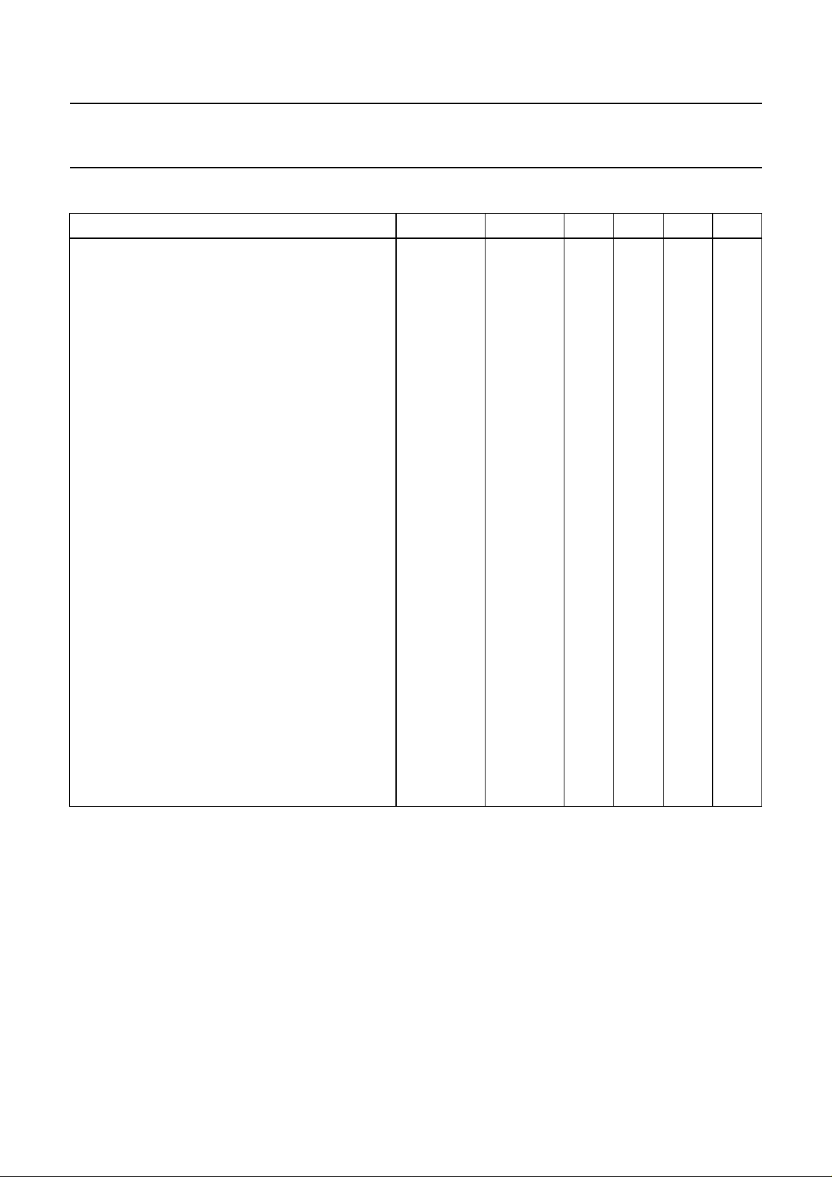
QUICK REFERENCE DATA
PARAMETER CONDITION SYMBOL MIN. TYP. MAX. UNIT
Supply
Minimum required current for starting
horizontal oscillator and output stage I
Main supply voltage V
Supply current I
Input signals
Sync pulse input amplitude V
Horizontal flyback pulse input current I
Vertical comparator input signal
Voltage AC V
Voltage DC V
Output signals
Horizontal output (open collector)
=25mA V
I
11
Vertical output stage driver
(emitter follower) I
= 1.5 mA V
1
Sandcastle output levels
V17 burst-key V
horizontal blanking V
vertical blanking V
Video transmitter identification output stage
(open collector loaded with external resistor to
positive supply). No sync. pulse present
Sync pulse present
divider ratio > 576 V
divider ratio < 576 V
16
10
12
V
I
13
10
5(p-p)
2
2
11
1
17
17
17
13
13
13
6.2 −−mA
− 12 − V
− 70 − mA
0.05 − 1.0 V
− 1 − mA
− 0.8 − V
− 1 − V
−−0.5 V
5 −−V
9.8 −−V
− 4.5 − V
− 2.5 − V
−−0.5 V
−−5mA
− V
10
− V
− 7.65 − V
September 1990 3
Page 4
Philips Semiconductors Preliminary specification
Horizontal/vertical synchronization circuit TDA2579B
September 1990 4
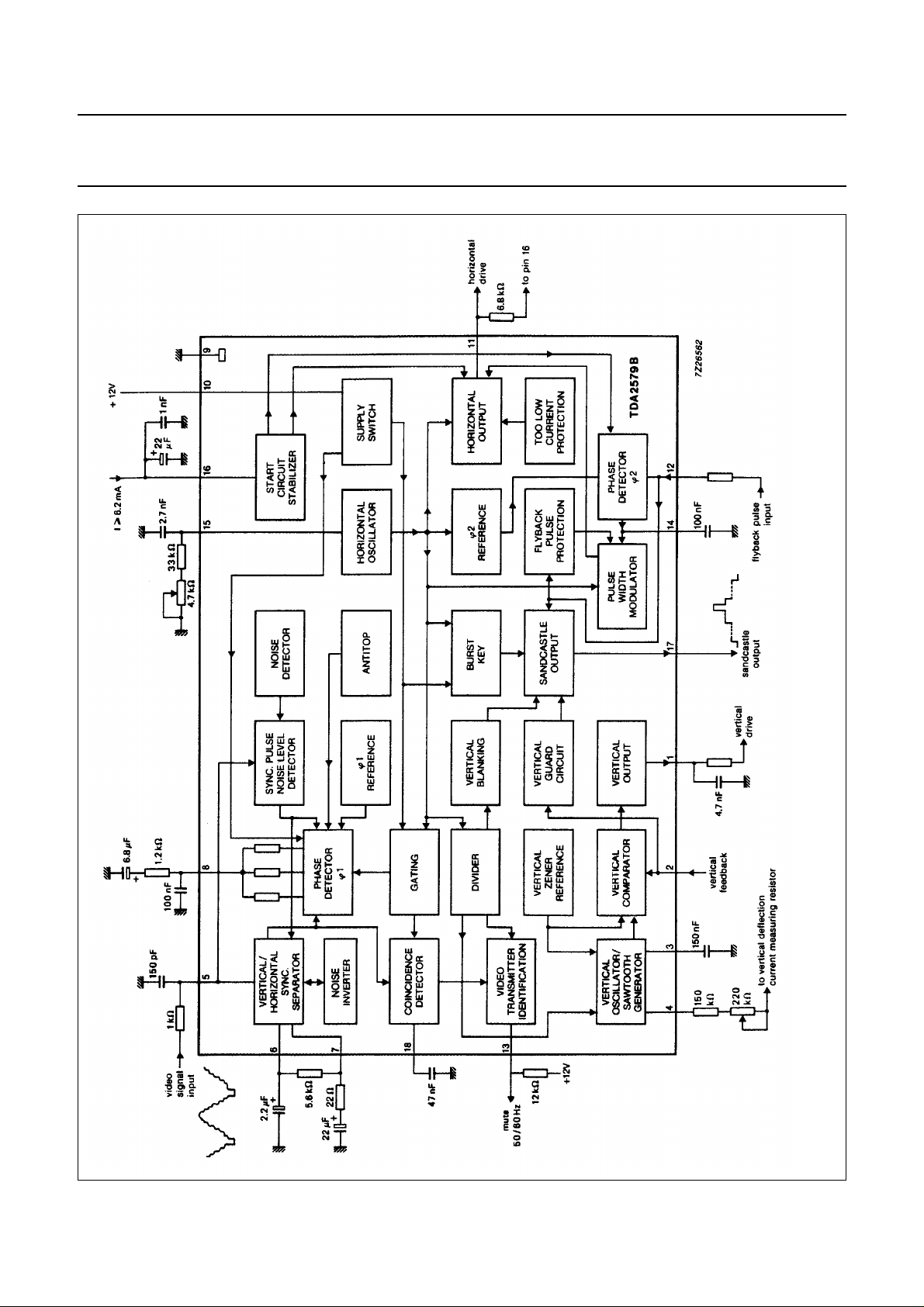
Fig.1 Block diagram.
Page 5

Philips Semiconductors Preliminary specification
Horizontal/vertical synchronization circuit TDA2579B
FUNCTIONAL DESCRIPTION
Vertical part (pins 1,2,3,4)
The IC embodies a synchronized divider system for generating the vertical sawtooth at pin 3. The divider system has an
internal frequency doubling circuit, so the horizontal oscillator is working at its normal line frequency and one line period
equals 2 clock pulses. Due to the divider system no vertical frequency adjustment is needed. The divider has a
discriminator window for automatically switching over from the 60 Hz to 50 Hz system. The divider system operates with
3 different divider reset windows for maximum interference/disturbance protection.
The windows are activated via an up/down counter. The counter increases its counter value by 1 for each time the
separated vertical sync pulse is within the searched window. The count is decreased by 1 when the vertical sync pulse
is not present.
Large (search) window: divider ratio between 488 and 722
This mode is valid for the following conditions:
1. Divider is looking for a new transmitter.
2. Divider ratio found, not within the narrow window limits.
3. Up/down counter value of the divider system operating in the narrow window mode decreases below count 1.
4. Externally setting. This can be reached by loading pin 18 with a resistor of 220 kΩ to earth or connecting a 3.6 V
diode stabistor between pin 18 and ground.
Narrow window: divider ratio between 522-528 (60 Hz) or 622-628 (50 Hz).
The divider system switches over to this mode when the up/down counter has reached its maximum value of 12 approved
vertical sync pulses. When the divider operates in this mode and a vertical sync pulse is missing within the window the
divider is reset at the end of the window and the counter value is decreased by 1. At a counter value below count 1 the
divider system switches over to the large window mode.
Standard TV-norm
When the up/down counter has reached its maximum value of 12 in the narrow window mode, the information applied to
the up/down counter is changed such that the standard divider ratio value is tested. When the counter has reached a
value of 14 the divider system is changed over to the standard divider ratio mode. In this mode the divider is always reset
at the standard value even if the vertical sync pulse is missing. A missed vertical sync pulse decreases the counter value
by 1. When the counter reaches the value of 10 the divider system is switched over to the large window mode.
The standard TV-norm condition gives maximum protection for video recorders playing tapes with anti-copy guards.
No-TV-transmitter found: (pin 18 < 1.2 V)
In this condition, only noise is present, the divider is rest to count 628. In this way a stable picture display at normal height
is achieved.
Video tape recorders in feature mode
It should be noted that some VTRs operating in the feature modes, such as picture search, generate such distorted
pictures that the no-TV-transmitter detection circuit can be activated as pin V
rolling picture (see Phase detector, sub paragraph d). In general VTR-machines use a re-inserted vertical sync pulse in
the feature mode. Therefore the divider system has been made such that the automatic reset of the divider at count 628
when V18 is below 1.2 V is inhibited when a vertical sync pulse is detected.
drops below 1.2 V. This would imply a
18
The divider system also generates the anti-top-flutter pulse which inhibits the Phase 1 detector during the vertical sync.
pulse. The width of this pulse depends on the divider mode. For the divider mode a the start is generated at the reset of
the divider. In mode b and c the anti-top-flutter pulse starts at the beginning of the first equalizing pulse.
September 1990 5
Page 6

Philips Semiconductors Preliminary specification
Horizontal/vertical synchronization circuit TDA2579B
The anti-top-flutter pulse ends at count 8 for 50 Hz and count 10 for 60 Hz. The vertical blanking pulse is also generated
via the divider system. The start is at the reset of the divider while the pulse ends at count 34 (17 lines) for 60 Hz, and at
count 44 (22 lines) for 50 Hz systems. The vertical blanking pulse generated at the sandcastle output pin 17 is made by
adding the anti-top-flutter pulse and the blanking pulse. In this way the vertical blanking pulse starts at the beginning of
the first equalizing pulse when the divider operates in the b or c mode. For generating a vertical linear sawtooth voltage
a capacitor should be connected to pin 3. The recommended value is 150 nF to 330 nF (see Fig.1).
The capacitor is charged via an internal current source starting at the reset of the divider system. The voltage on the
capacitor is monitored by a comparator which is activated also at reset. When the capacitor has reached a voltage value
of 5.85 V for the 50 Hz system or 4.85 V for the 60 Hz system the voltage is kept constant until the charging period ends.
The charge period width is 26 clock pulses. At clock pulse 26 the comparator is switched off and the capacitor is
discharged by an npn transistor current source, the value of which can be set by an external resistor between pin 4 and
ground (pin 9). Pin 4 is connected to a pnp transistor current source which determines the current of the npn current
source at pin 3. The pnp current source on pin 4 is connected to an internal zener diode reference voltage which has a
typical voltage of ≈7.5 volts. The recommended operating current range is 10 to 75 µA. The resistance at pin R4 should
be 100 to 770 kΩ. By using a double current mirror concept the vertical sawtooth pre-correction can be set on the desired
value by means of external components between pin 4 and pin 3, or by connecting the pin 4 resistor to the vertical current
measuring resistor of the vertical output stage. The vertical amplitude is set by the current of pin 4. The vertical feedback
voltage of the output stage has to be applied to pin 2. For the normal amplitude adjustment the values are DC = 1 V and
AC = 0.8 V. Due to the automatic system adaption both values are valid for 50 Hz and 60 Hz.
The low DC voltage value improves the picture bounce behaviour as less parabola compensation is necessary. Even a
fully DC coupled feedback circuit is possible.
Vertical guard
The IC also contains a vertical guard circuit. This circuit monitors the vertical feedback signal on pin 2. When the level
on pin 2 is below 0.35 V or higher than 1.85 V the guard circuit inserts a continuous level of 2.5 V in the sandcastle output
signal of pin 17. This results in the blanking of the picture displayed, thus preventing a burnt-in horizontal line. The guard
levels specified refer to the zener diode reference voltage source level.
Driver output
The driver output is at pin 1, it can deliver a drive current of 1.5 mA at 5 V output. The internal impedance is approximately
170 Ω. The output pin is also connected to an internal current source with a sink current of 0.25 mA.
Sync separator, phase detector and TV-station identification (pins 5,6,7,8 and 18)
The video input signal is connected to pin 5. The sync separator is designed such that the slicing level is independent of
the amplitude of the sync pulse. The black level is measured and stored in the capacitor at pin 7. The slicing level value
is stored in the capacitor at pin 6. The slicing level value can be chosen by the value of the external resistor between
pins 6 and 7. The value is given by the formula:
R
s
P
---------------------
5.3 Rs+
Where R
100 R
is the resistor between pins 6 and 7 and top sync level equals 100%. The recommended resistor value
s
value in kΩ()×=
s
is 5.6 kΩ.
September 1990 6
Page 7

Philips Semiconductors Preliminary specification
Horizontal/vertical synchronization circuit TDA2579B
Black level detector
A gating signal is used for the black level detector. This signal is composed of an internal horizontal reference pulse with
a duty factor of 50% and the flyback pulse at pin 12. In this way the TV-transmitter identification operates also for all DC
conditions at input pin 5 (no video modulation, plain carrier only).
During the frame interval the slicing level detector is inhibited by a signal which starts with the anti-top flutter pulse and
ends with the reset vertical divider circuit. In this way shift of the slicing level due to the vertical sync signal is reduced
and separation of the vertical sync pulse is improved.
Noise level detector
An internal noise inverter is activated when the video level at pin 5 decreases below 0.7 V. The IC also embodies a
built-in sync pulse noise level detection circuit. This circuit is directly connected to pin 5 and measures the noise level at
the middle of the horizontal sync pulse. When a signal-to-noise level of 19 dB is detected a counter circuit is activated.
A video input signal is processed as “acceptable noise free” when 12 out of 15 sync pulses have a noise level below
19 dB for two successive frame periods. The sync pulses are processed during a 15 line width gating period generated
by the divider system. The measuring circuit has a built-in noise level hysteresis of approximately 3 dB. When the
“acceptable noise free” condition is found the phase detector of pin 8 is switched to not gated and normal time constant.
When a higher sync pulse noise level is found the phase detector is switched over to slow time constant and gated sync
pulse phase detection. At the same time the integration time of the vertical sync pulse separator is adapted.
SN⁄ 20 Log
=
Video voltage black to white
---------------------------------------------------------------------------------------------------
()
Noise
rms
p-p
Phase detector
The phase detector circuit is connected to pin 8. This circuit consists of 3 separate phase detectors which are activated
depending on the voltage of pin 18 and the state of the sync pulse noise detection circuit. For normal and fast time
constants all three phase detectors are activated during the vertical blanking period, this with the exception of the
anti-top-flutter pulse period, and the separated vertical sync-pulse time. As a result, phase jumps in the video signal
related to the video head, take over of video recorders are quickly restored within the vertical blanking period. At the end
of the blanking period the phase director time constant is increased by 1.5 times. In this way there is no requirement for
external VTR time constant switching, and so all station numbers are suitable for signals from VTR, video games or home
computers.
For quick locking of a new TV station starting from a noise only signal condition (normal time constant) a special circuit
is incorporated. A new TV station which is not locked to the horizontal oscillator will result in a voltage decrease below
0.1 V at pin 18. This will activate a frame period counter which switches the phase detector to fast for 3 frame periods
during the vertical scan period.
The horizontal oscillator will now lock to the new TV-station and as a result, the voltage on pin 18 will increase to
approximately 6.5 V. When pin 18 reaches a level of 1.8 V the mute output transistor of pin 13 is switched OFF and the
divider is set to the large window. In general the mute signal is switched OFF within 5 ms (pin C
= 47 nF) after reception
18
of a new TV-signal. When the voltage on pin 18 reaches a level of 5 V, usually within 15 ms, the frame counter is switched
OFF and the time constant is switched from fast to normal during the vertical scan period.
September 1990 7
Page 8
Philips Semiconductors Preliminary specification
Horizontal/vertical synchronization circuit TDA2579B
If the new TV station is weak, the sync-noise detector is activated. This will result in a change over of pin 18 voltage from
6.5 V to ≈10 V. When pin 18 exceeds the level of 7.8 V the phase detector is switched to slow time constant and gated
sync pulse condition. The current is also reduced during the vertical blanking period by 1 mA. When desired, most
conditions of the phase detector can also be set by external means in the following way:
a. Fast time constant TV transmitter identification circuit not active, connect pin 18 to earth (pin 9).
b. Fast time constant TV transmitter identification circuit active, connect a resistor of 220 kΩ between pin 18 and ground.
This condition can also be set by using a 3.6 V stabistor diode instead of a resistor.
c. Slow time constant, (with exception of frame blanking period), connect pin 18 via a resistor of 10 kΩ to + 12 V, pin 10.
In this condition the transmitter identification circuit is not active.
d. No switching to slow time constant desired (transmitter identification circuit active), connect a 6.8 V zener diode
between pin 18 and ground.
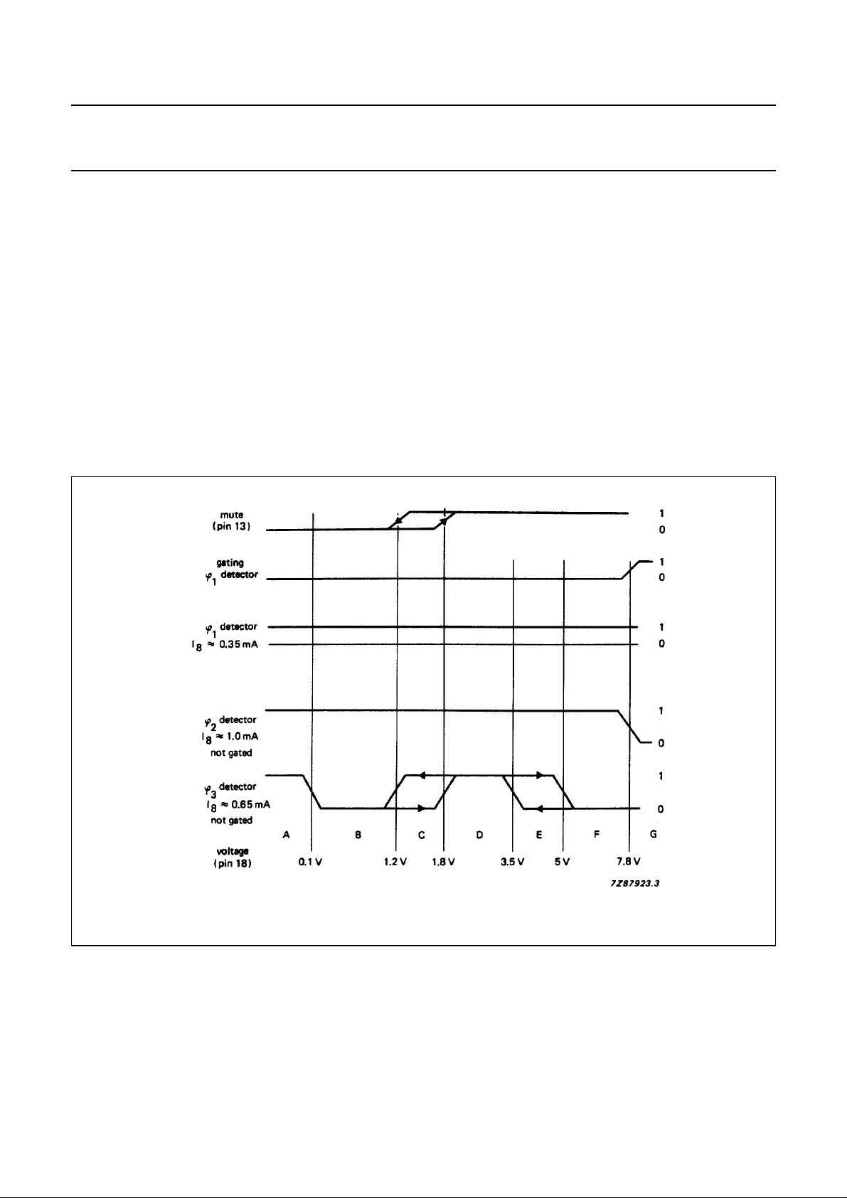
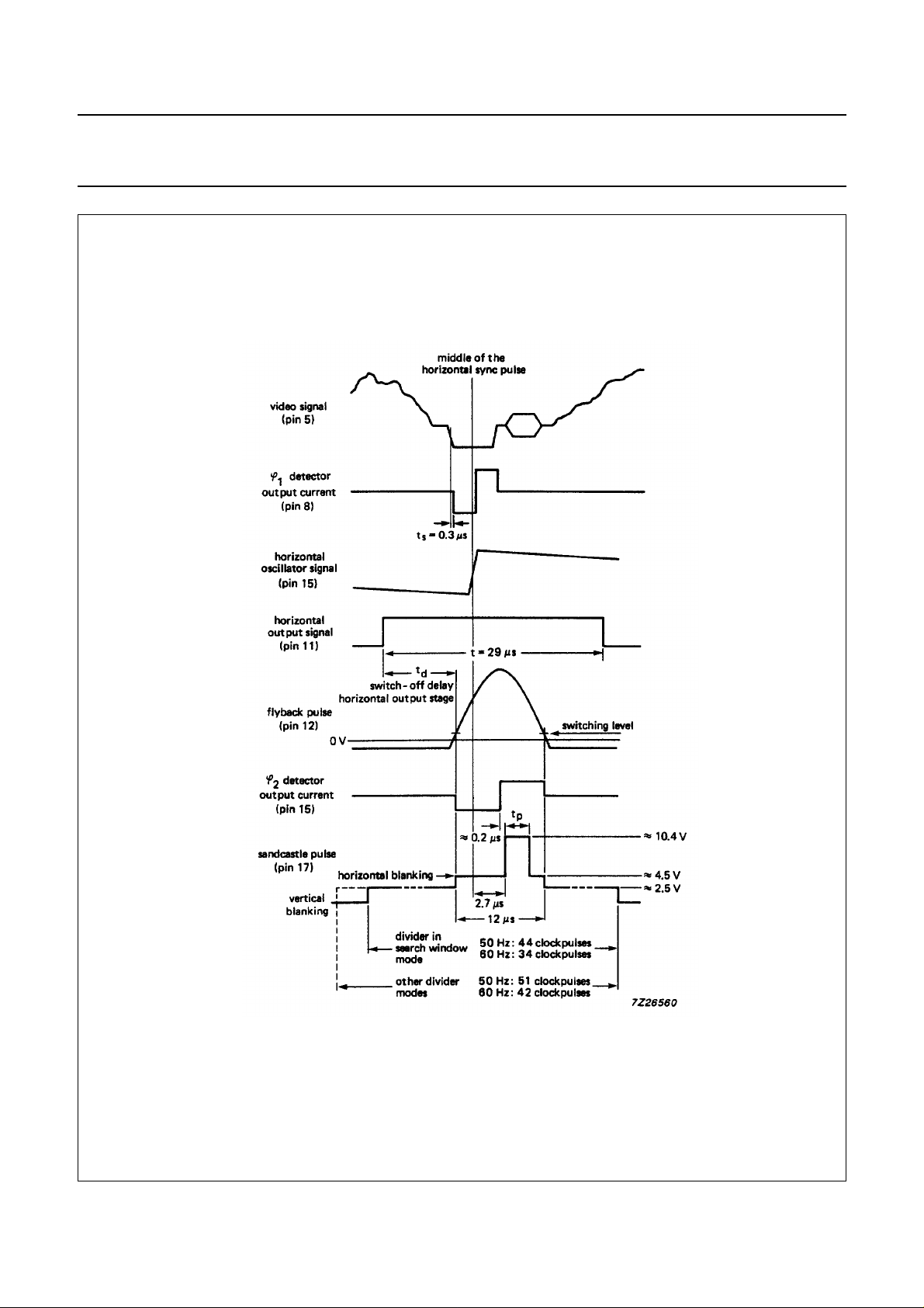
Fig.2 illustrates the operation of the 3 phase detector circuits.
Fig.2 Timing diagram, phase detectors.
September 1990 8
Page 9

Philips Semiconductors Preliminary specification
Horizontal/vertical synchronization circuit TDA2579B
Supply (pins 9, 10 and 16) The IC has been designed such that the horizontal oscillator and output stage can start operating by application of a very
low supply current into pin 16.
The horizontal oscillator starts at a supply current of approximately 4 mA. The horizontal output stage is forced into the
non-conducting stage until the supply current has a typical value of 5 mA. The circuit has been designed so that after
starting the horizontal output function a current drop of ≈ 1 mA is allowed. The starting circuit has the ability to derive the
main supply (pin 10) from the horizontal output stage. The horizontal output signal can also be used as the oscillator
signal for synchronized switched mode power supplies. The maximum allowed starting current is 9.7 mA (T
The main supply should be connected to pin 10, and pin 9 should be used as ground. When the voltage on pin 10
increases from zero to its final value (typically 12 V) a part of the supply current of the starting circuit is taken from pin 10
via internal diodes, and the voltage on pin 16 will stabilize to a typical value of 9.4 V.
In a stabilized condition (pin V10> 10 V) the minimum required supply current to pin 16 is ≈ 2.5 mA. All other IC functions
are switched on via the main supply voltage on pin 10. When the voltage on pin 10 reaches a value of ≈ 7 V the horizontal
phase detector circuit is activated and the vertical ramp on pin 3 is started. The second phase detector circuit and burst
pulse circuit are started when the voltage on pin 10 reaches the stabilized voltage value of pin 16 which is typically 9.4 V.
To close the second phase detector loop, a flyback pulse must be applied to pin 12. When no flyback pulse is detected
the duty factor of the horizontal output stage is 50%.
amb
=25°C).
For remote switch-off pin 16 can be connected to ground (via a npn transistor with a series resistor of ≈ 500 Ω) which
switches off the horizontal output.
Horizontal oscillator, horizontal output transistor, and second phase detector (pins 11, 12, 14 and 15) The horizontal oscillator is connected to pin 15. The frequency is set by an external RC combination between pin 15 and
ground, pin 9. The open collector horizontal output stage is connected to pin 11. An internal zener diode configuration
limits the open voltage of pin 11 to ≈ 14.5 V.
The horizontal output transistor at pin 11 is blocked until the current into pin 16 reaches a value of ≈ 5 mA.
A higher current results in a horizontal output signal at pin 11, which starts with a duty factor of ≈ 40% HIGH.
The duty factor is set by an internal current-source-loaded npn emitter follower stage connected to pin 14 during starting.
When pin 16 changes over to voltage stabilization the npn emitter follower and current source load at pin 14 are switched
OFF and the second phase detector circuit is activated, provided a horizontal flyback pulse is present at pin 12.
When no flyback pulse is detected at pin 12 the duty factor of the horizontal output stage is set to 50%.
The phase detector circuit at pin 14 compensates for storage time in the horizontal deflection output stage. The horizontal
output pulse duration is 29 µs HIGH for storage times between 1 µs and 17 µs (flyback pulse of 12 µs). A higher storage
time increases the HIGH time. Horizontal picture shift is possible by forcing an external charge or discharge current into
the capacitor at pin 14.
September 1990 9
Page 10

Philips Semiconductors Preliminary specification
Horizontal/vertical synchronization circuit TDA2579B
Mute output and 50/60 Hz identification (pin 13)
The collector of an npn transistor is connected to pin 13. When the voltage on pin 18 drops below 1.2 V
(no TV-transmitter) the npn transistor is switched ON.
When the voltage on pin 18 increases to a level of ≈ 1.8 V (new TV-transmitter found) the npn transistor is switched OFF.
Pin 13 has also the possibility for 50/60 Hz identification. This function is available when pin 13 is connected to pin 10
(+ 12 V) via an external pull-up resistor of 10 to 20 kΩ. When no TV-transmitter is identified the voltage on pin 13 will be
LOW (< 0.5 V). When a TV-transmitter with a divider ratio > 576 (50 Hz) is detected the output voltage of pin 13 is HIGH
(+ 12 V).
When a TV-transmitter with a divider ratio < 576 (60 Hz) is found an internal pnp transistor with its emitter connected to
pin 13 will force this pin output voltage down to ≈ 7.6 V.
Sandcastle output (pin 17) The sandcastle output pulse generated at pin 17, has three different voltage levels. The highest level, (10.4 V), can be
used for burst gating and black level clamping. The second level (4.5 V) is obtained from the horizontal flyback pulse at
pin 12, and is used for horizontal blanking. The third level (2.5 V) is used for vertical blanking and is derived via the
vertical divider system. For 50 Hz the blanking pulse duration is 44 clock pulses and for 60 Hz it is 34 clock pulses started
from the vertical divider reset. For TV-signals which have a divider ratio between 622 and 628 or between 522 and 528
the pulse is started at the first equalizing pulse. With the 50/60 Hz information the burst-key pulse width is switched to
improve the behaviour in multi-norm concepts.
September 1990 10
Page 11

Philips Semiconductors Preliminary specification
Horizontal/vertical synchronization circuit TDA2579B
RATINGS
Limiting values in accordance with Absolute Maximum System (IEC 134)
PARAMETER SYMBOL MIN. MAX. UNIT
Start current I
Supply voltage V
Total power dissipation P
Storage temperature range T
Operating ambient temperature range T
Thermal resistance
16
10
tot
stg
amb
− 9.7 mA
− 13.2 V
− 1.2 W
−55 + 150 °C
−25 + 70 °C
From junction to ambient in free air R
th j-a
50 K/W
September 1990 11
Page 12

Philips Semiconductors Preliminary specification
Horizontal/vertical synchronization circuit TDA2579B
CHARACTERISTICS
=25°C; I16= 6.2 mA; V10= 12 V; unless otherwise specified
T
amb
Voltage measurements are taken with respect to pin 9 (ground)
PARAMETER CONDITIONS SYMBOL MIN. TYP. MAX. UNIT
Supply
Supply current (pin 16)
=0V I
V
10
V
=10V I
10
Stabilized voltage (pin 16) V
Current consumption (pin 10) I
Supply voltage range (pin 10) V
16
16
16
10
P
Video input (pin 5)
Top sync level V
5
Sync pulse amplitude
(peak-to-peak value) note 1 V
5(p-p)
Slicing level note 2 35 50 65 %
Delay between video input
and detector output
(see also Fig.3) 0.2 0.3 0.55 µs
Sync pulse noise level
detector circuit active note 3 S/N − 19 − dB
6.2 − 9.7 mA
2.5 − 9.7 mA
8.8 9.3 9.7 V
− 70 85 mA
10 12 13.2 V
1.5 3.1 3.75 V
0.05 0.6 1.0 V
Sync pulse
Noise level detector circuit hysteresis − 3 − dB
Noise gate (pin 5)
Switching level V
5
−+0.7 + 1V
First control loop (pin 8)
(horizontal oscillator to sync)
Holding range ∆ f −±800 Hz
Catching range ∆ f ± 700 ±800 ±1100
Control sensitivity video
with respect to burst-key
and flyback-pulse
Slow time constant − 2 − kHz/µs
Normal time constant − 5 − kHz/µs
Fast time constant − 3 − kHz/µs
Phase modulation due to hum on
the supply line (pin 10) note 4 − 0.2 −µs/Vtt
Phase modulation due to hum on
input current (pin 16) note 4 − 0.08 −µs/Vtt
September 1990 12
Page 13
Philips Semiconductors Preliminary specification
Horizontal/vertical synchronization circuit TDA2579B
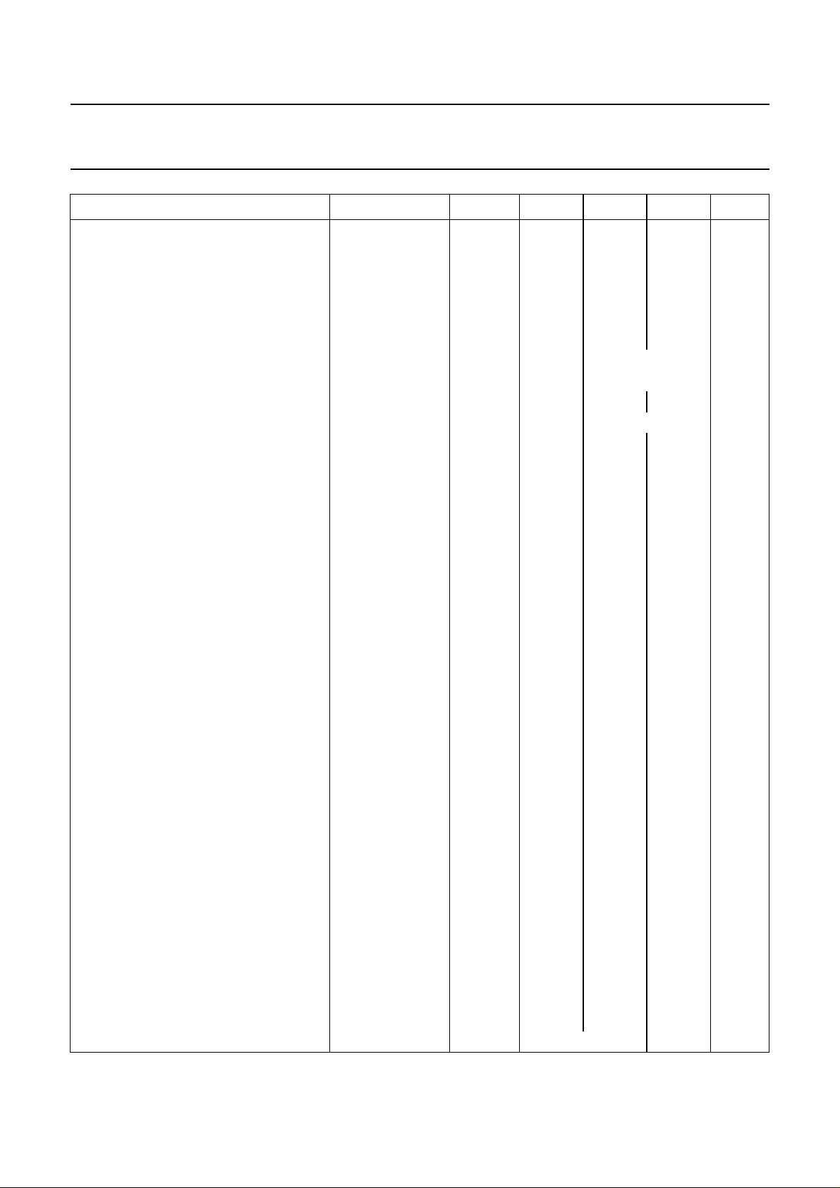
PARAMETER CONDITIONS SYMBOL MIN. TYP. MAX. UNIT
Second control loop (pin 14)
(horizontal flyback to horizontal
oscillator)
Control sensitivity t
Control range t
Control range for constant duty
factor horizontal output t
Controlled edge of horizontal
output signal (pin 11) positive
Phase adjustment (pin 14)
(via second control loop)
Control sensitivity t
Maximum allowed control current I
Horizontal oscillator (pin 15)
Frequency (no sync) f − 15625 − Hz
Spread (fixed external component,
no sync) ∆ f −−±4%
Frequency deviation between
starting point output signal
and stabilized condition ∆ f −+5+8%
Temperature coefficient T
Horizontal output (pin 11)
(Open collector)
Output voltage high V
Start voltage protection
(internal zener diode) V
Low input current (pin 16)
protection output enabled I
Output voltage low start condition I
Duty factor output current
during starting I
Output voltage low normal
condition I
Duty factor output current
without flyback pulse (pin 12) 45 50 55 %
Duration of the output pulse HIGH t
Controlled edge positive
=10µs ∆td/∆to200 300 600 µs
d
d
d
=10µs − 25 −µA/µs
d
14
1 −>45 µs
1 29 (−t flyback
pulse)
µs
−−±60 µA
C = 2.7 nF;
R
= 34.8 kΩ
osc
C
11
11
16
=10mA V
11
= 6.2 mA 50 60 70 %
16
=25mA V
11
=10µs 272931µs
d
11
11
−−1.10
−−13.2 V
13 − 15.8 V
− 5.0 6.2 mA
− 0.1 0.5 V
− 0.3 0.5 V
-4
− /K
September 1990 13
Page 14

Philips Semiconductors Preliminary specification
Horizontal/vertical synchronization circuit TDA2579B
PARAMETER CONDITIONS SYMBOL MIN. TYP. MAX. UNIT
Temperature coefficient
horizontal output pulse −−5.10
Influence of delay time on pulse
width of the horizontal output
signal ∆H
=1mA
I
Sandcastle output signal (pin 17)
L
W/td
− 0.16 −µs/µs
Output voltage during:
burst-key V
horizontal blanking V
vertical blanking I
Zero level output voltage I
= 0.3 mA V
L
= 0.5 mA V
sink
17
17
17
17
9.8 10.4 − V
4.1 4.5 4.9 V
2.1 2.5 2.9 V
−−0.7 V
Pulse width:
burst-key (50 Hz) t
burst-key (60 Hz) t
Horizontal blanking V
p
p
12
3.85 4.15 4.6 µs
3.40 3.65 4.0 µs
− 1.0 − V
Vertical blanking note 5
Phase position burstkey
time between middle sync
pulse at pin 5 and start of
burst pulse at pin 17 2.3 2.7 3.1 µs
Time between start sync pulse
and end of burst pulse at pin 17
(50 Hz) − 9.3 9.7 µs
(60 Hz) − 8.8 9.2 µs
-2
−µs/°C
Coincidence detector, video transmitter
identification circuit and time constant
switching levels (see also Fig.1)
Detector output current I
Voltage level for in sync
condition (ϕ1 normal) V
Voltage for noisy sync pulse
(ϕ1 slow and gated) V
Voltage level for noise only note 6 V
Switching level normal to fast V
Switching level
mute output active and
fast to normal V
Switching level frame period
counter (3 periods fast) V
September 1990 14
18
18
18
18
18
18
18
− 0.25 − mA
5.8 6.5 7.0 V
910−V
− 0.3 − V
< 3.2 3.5 3.8 V
< 1.0 1.2 1.4 V
< 0.08 0.12 0.16 V
Page 15

Philips Semiconductors Preliminary specification
Horizontal/vertical synchronization circuit TDA2579B
PARAMETER CONDITIONS SYMBOL MIN. TYP. MAX. UNIT
Switching level:
normal to fast (locking)
mute output inactive V
Switching level fast to normal
(locking) V
Switching level normal to slow
(gated sync pulse) V
Video transmitter identification output
(pin 13)
Output voltage active
(no sync) I
= 1 mA V
13
Sink current active
(no sync) V13< 1V I
Output current inactive
(sync 50 Hz) I
50/60 Hz identification (pin 13)
(R13 positive supply 12 kΩ)
Emitter follower, pnp:
18
18
18
13
13
13
> 1.5 1.75 2.0 V
> 4.7 5.0 5.3 V
7.4 7.8 8.2 V
− 0.15 0.32 V
−−5mA
−−1µA
60 Hz: < 576 voltage
50 Hz: > 576 voltage
2f
×
-------------f
V
×
2f
H
-------------f
V
H
V
13
V
13
7.2 7.65 8.1 V
− V
10
− V
Flyback input pulse (pin 12)
Switching level V
Input current I
Input pulse V
12
12
12
−+1−V
+0.2 −+3mA
−−12 V
P
Input resistance − 3.5 − kΩ
Phase position without shift
time between the middle of the
sync pulse at pin 5 and the
middle of the horizontal
blanking pulse at pin 17 t
d
2.1 2.5 2.9 µs
Vertical ramp generator (pin 3)
Pulse width charge current −−26 − clock
pulses
Charge current I
3
− 3 − mA
Top level ramp signal voltage
Divider in 50 Hz mode note 7 V
Divider in 60 Hz mode note 7 V
3
3
5.5 5.85 6.3 V
4.55 4.85 5.25 V
September 1990 15
Page 16

Philips Semiconductors Preliminary specification
Horizontal/vertical synchronization circuit TDA2579B
PARAMETER CONDITIONS SYMBOL MIN. TYP. MAX. UNIT
Ramp amplitude C
R
= 330 kΩ 50 Hz note 7 − 3.1 − V
4
R4= 330 kΩ 60 Hz note 7 − 2.5 − V
Temperature coefficient I4=30µAI
Current source (pin 4)
Output voltage I4=20µAV
Allowed current range I
Temperature coefficient
output voltage I
Comparator (pin 2)
Input voltage
DC level note 7 V
AC level V
Deviation amplitude 50/60 Hz − 1.75 2.5 %
= 150 nF,
3
3
4
4
=30µATC−+50 − 10-6/K
4
C
= 150 nF;
3
= 330 kΩ
R
4
2
2
−+100 − 10-6/K
7.0 7.5 7.9 V
10 − 75 µA
0.97 1.07 1.17 V
− 0.8 − V
P
P
P
Vertical output stage (pin 1)
(npn emitter follower)
Output voltage I
R
sync separator resistor − 170 −Ω
s,
pin 1 = +1.5 mA
o
note 7 V
1
5.0 5.5 6.3 V
Continuous sink current − 0.25 − mA
Vertical guard circuit (pin 2)
Active (V
Switching level LOW note 7 V
Switching level HIGH note 7 V
= 2.5 V)
17
2
2
> 1.7 1.85 2.0 V
< 0.25 0.35 0.45 V
Notes
1. Up to 1 V peak-to-peak the slicing level is constant, at amplitudes exceeding 1 V peak-to-peak the slicing level will
increase.
2. The slicing level is fixed by the formula:
R
s
P
---------------------
5.3 Rs+
SN⁄ 20
3.
measured with 1 V
100% R
video voltage black to white (p-p)
---------------------------------------------------------------------------------------log=
p-p
value in kΩ()×=
s
noise rms()
video input
4. Measured between pin 5 and sandcastle output pin 17.
September 1990 16
Page 17

Philips Semiconductors Preliminary specification
Horizontal/vertical synchronization circuit TDA2579B
5. Divider in search (large) mode:
start: reset divider = start vertical sync plus 1 clock pulse stop:
2f
×
H
-------------f
V
2f
×
H
-------------f
V
> 576 clock pulse 44=
< 576 clock pulse 34=
≈ 5V.
5
n
n
Divider in small window mode:
start: clock pulse 517 (60 Hz) clock pulse 618 (50 Hz)
stop: clock pulse 34 (60 Hz) clock pulse 44 (50 Hz)
6. Depends on DC level of pin 5, given value is valid for V
7. Value related to internal zener diode reference voltage source spread includes the complete spread of reference
voltage.
September 1990 17
Page 18
Philips Semiconductors Preliminary specification
Horizontal/vertical synchronization circuit TDA2579B
Fig.3 Timing diagram of the TDA2579B.
September 1990 18
Page 19
Philips Semiconductors Preliminary specification
Horizontal/vertical synchronization circuit TDA2579B
APPLICATION INFORMATION
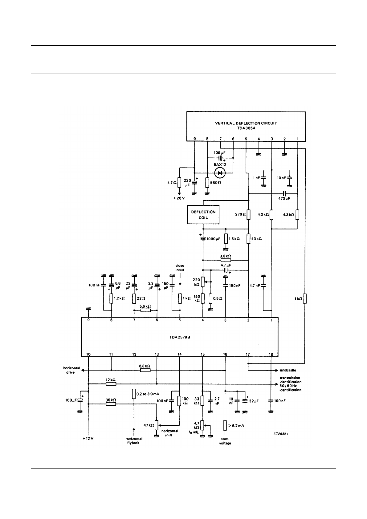
Fig.4 TDA2579B 110° application circuit (45AX).
September 1990 19
Page 20
Philips Semiconductors Preliminary specification
Horizontal/vertical synchronization circuit TDA2579B
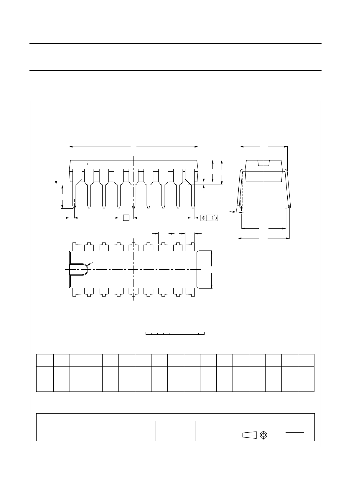
PACKAGE OUTLINE
DIP18: plastic dual in-line package; 18 leads (300 mil)
D
seating plane
L
Z
18
pin 1 index
e
b
SOT102-1
M
E
A
2
A
A
1
w M
b
1
b
2
10
E
c
(e )
1
M
H
1
0 5 10 mm
scale
DIMENSIONS (inch dimensions are derived from the original mm dimensions)
A
A
A
UNIT
max.
mm
inches
Note
1. Plastic or metal protrusions of 0.25 mm maximum per side are not included.
OUTLINE
VERSION
SOT102-1
12
min.
max.
IEC JEDEC EIAJ
b
1.40
1.14
0.055
0.044
b
1
0.53
0.38
0.021
0.015
b
cD E e M
2
0.32
1.40
0.23
1.14
0.013
0.055
0.009
0.044
REFERENCES
21.8
21.4
0.86
0.84
September 1990 20
9
(1) (1)
6.48
6.20
0.26
0.24
L
e
1
M
3.9
8.25
3.4
7.80
0.15
0.32
0.13
0.31
EUROPEAN
PROJECTION
E
9.5
8.3
0.37
0.33
H
0.2542.54 7.62
0.010.10 0.30
ISSUE DATE
w
93-10-14
95-01-23
max.
0.854.7 0.51 3.7
0.0330.19 0.020 0.15
(1)
Z
Page 21
Philips Semiconductors Preliminary specification
Horizontal/vertical synchronization circuit TDA2579B
SOLDERING
Introduction
There is no soldering method that is ideal for all IC packages. Wave soldering is often preferred when through-hole and
surface mounted components are mixed on one printed-circuit board. However, wave soldering is not always suitable for
surface mounted ICs, or for printed-circuits with high population densities. In these situations reflow soldering is often
used.
This text gives a very brief insight to a complex technology. A more in-depth account of soldering ICs can be found in our
“IC Package Databook”
Soldering by dipping or by wave
The maximum permissible temperature of the solder is 260 °C; solder at this temperature must not be in contact with the
joint for more than 5 seconds. The total contact time of successive solder waves must not exceed 5 seconds.
The device may be mounted up to the seating plane, but the temperature of the plastic body must not exceed the
specified maximum storage temperature (T
be necessary immediately after soldering to keep the temperature within the permissible limit.
(order code 9398 652 90011).
). If the printed-circuit board has been pre-heated, forced cooling may
stg max
Repairing soldered joints
Apply a low voltage soldering iron (less than 24 V) to the lead(s) of the package, below the seating plane or not more
than 2 mm above it. If the temperature of the soldering iron bit is less than 300 °C it may remain in contact for up to
10 seconds. If the bit temperature is between 300 and 400 °C, contact may be up to 5 seconds.
DEFINITIONS
Data sheet status
Objective specification This data sheet contains target or goal specifications for product development.
Preliminary specification This data sheet contains preliminary data; supplementary data may be published later.
Product specification This data sheet contains final product specifications.
Limiting values
Limiting values given are in accordance with the Absolute Maximum Rating System (IEC 134). Stress above one or
more of the limiting values may cause permanent damage to the device. These are stress ratings only and operation
of the device at these or at any other conditions above those given in the Characteristics sections of the specification
is not implied. Exposure to limiting values for extended periods may affect device reliability.
Application information
Where application information is given, it is advisory and does not form part of the specification.
LIFE SUPPORT APPLICATIONS
These products are not designed for use in life support appliances, devices, or systems where malfunction of these
products can reasonably be expected to result in personal injury. Philips customers using or selling these products for
use in such applications do so at their own risk and agree to fully indemnify Philips for any damages resulting from such
improper use or sale.
September 1990 21
 Loading...