

Page 1
IF AMPLIFIERWITHDEMODULATOR AND AFC
.
SUPPLYVOLTAGE: 12V TYP
.
SUPPLYCURRENT : 50mATYP
.
I.F. INPUT VOLTAGE SENSITIVITY AT
PP
RMS
TYP
TYP
F =38.9MHz :85µV
.
VIDEO OUTPUT VOLTAGE (white at 10% of
top synchro): 2.7V
.
I.F. VOLTAGE GAIN CONTROL RANGE :
64dB TYP
.
SIGNAL TO NOISE RATIO AT VI= 10mV :
58dB TYP
.
A.F.C. OUTPUT VOLTAGE SWING FOR
∆f = 100kHz: 10V TYP
DESCRIPTION
The TDA2540and 2541 are IF amplifier and A.M.
demodulatorcircuitsfor colourandblackand white
televisionreceiversusingPNPorNPNtuners.They
are intended for reception of negative or positive
modulationCCIR standard.
They incorporatethe followingfunctions :
.
Gaincontrolled amplifier
.
Synchronousdemodulator
.
Whitespot inverter
.
Video preamplifier with noise protection
.
SwitchableAFC
.
AGCwith noise gating
.
Tuner AGC output (NPN tuner for 2540)-(PNP
tuner for 2541)
.
VCR switch for video output inhibition (VCR
play back)
TDA2540
TDA2541
DIP16
(Plastic Package)
ORDER CODE : TDA2540-TDA2541
PIN CONNECTIONS
DECOUPLINGCAPACITOR
TUNER AGC TAKE-OVERADJUST
TUNERAGC OUTPUT
AFC DEMODULATOR L.C. NETWORK
REFERENCEL.C. NETWORK
August 1992
IF INPUT
AFCOUTPUT
AFC SWITCH
1
2
3
4
5
6
7
8
16
15
14
13
12
11
10
IF INPUT
DECOUPLINGCAPACITOR
AGC CAPACITOR
GROUND
VIDEO OUTPUT
V
CC
AFCDEMODULATORL.C. NETWORK
9
REFERENCEL.C. NETWORK
2540-01.EPS
1/7
Page 2

TDA2540 - TDA2541
BLOCK DIAGRAM
ABSOLUTE MAXIMUMRATINGS
Symbol Parameter Value Unit
V (11–13) Supply Voltage 13.8 V
V (4–13) Tuner A.G.C. Voltage 12 V
T
P
T
tot
stg
amb
Power Dissipation 900 mW
Storage Temperature – 55 to + 125 °C
Operating Ambient Temperature 0 to + 70 °C
THERMALDATA
Symbol Parameter Value Unit
R
th (j-a)
Junction - ambient Thermal Resistance 70 °C/W
ELECTRICAL OPERATING CHARACTERISTICS
=25oC;V
T
amb
Symbol Parameter Min. Typ. Max. Unit
V
11-13
I
V
11
1-16
Supply Voltage Range 10.2 12 13.8 V
Supply Current 50 60 mA
IF Input Voltage Sensitivity 60 85 180 µV
Max Input Voltage (Pins 1-16) 140 mV
V
V
V
12-13
Z
12-13
12-13
∆G
1-16
Video Output Voltage 2.7 V
Differential Input Impedance (in parallel with 2pF) 2 kΩ
Zero Signal Output Level 5.7 6 6.3 V
Top Synchro Output Level 2.9 3.07 3.2 V
IF Voltage Gain Control Range 52 64 dB
V
=12V; f =38.9MHz (unless otherwise specified)
11–13
2540-02.TIF
2540-01.TBL
2540-02.TBL
RMS
pp
2540-03.TBL
2/7
Page 3
TDA2540- TDA2541
ELECTRICAL OPERATING CHARACTERISTICS (continued)
=25°C; V (11 – 13) = 12 V; f = 38.9 MHz (unlessotherwise specified)
T
amb
Symbol Parameter Min. Typ. Max. Unit
S/N Signal to Noise Ratio (V
B Bandwidth of Video Amplifier (– 3dB) 6 MHz
dG Differential Gain 4 10 %
dφ Differential Phase 2 10 %
V
V
12-13
12-13
Carrier Signal at Video Output (VI= 10mV) 4 30 mV
2nd Harmonic of Carrier at Video Output (VI= 10mV) 20 30 mV
Intermodulation at 1.1MHz (blue) (see Figures 2 and 3) 46 60 dB
Intermodulation at 1.1MHz (yellow) (see Figures 2 and 3) 46 50 dB
Intermodulation at 3.3MHz (blue) (see Figures 2 and 3) 46 54 dB
V
14-13
VCR Switches Off Output at : (VCR = low Level) 1.1 V
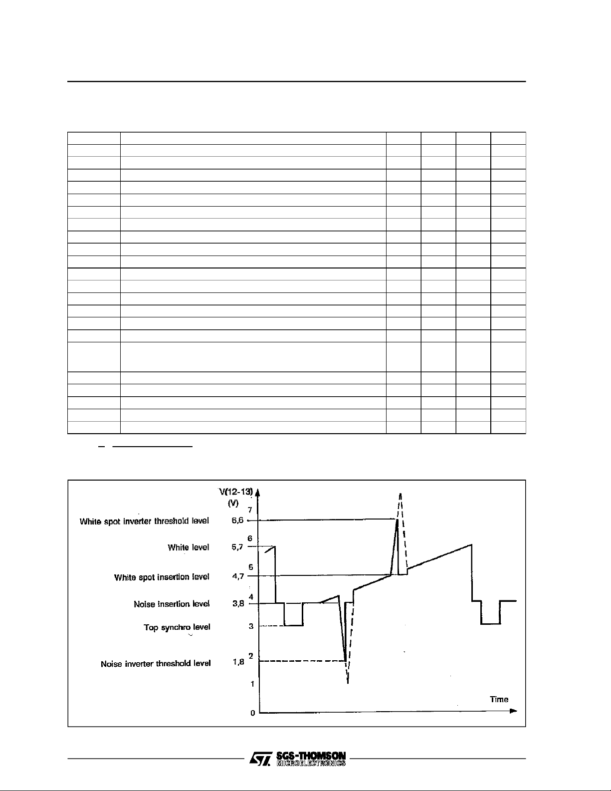
White Spot Inverter Threshold Level (see Figure 1) 6.6 V
White Spot Insertion Level (see Figure 1) 4.7 V
Noise Inverter Threshold Level (see Figure 1) 1.8 V
Noise Insertion Level (see Figure 1) 3.8 V
V
I
4
14-13
I
4
Tuner AGC output Current Range 0 to 10 mA
Tuner AGC Output Voltage 0.3 V
Tuner AGC Output Leakage Current
TDA2541 V
TDA2540 V
∆V
5-13
AFC Output Voltage Swing (∆f = 100 kHz) 10 11 V
∆f Change of Frequency at AFC Output (voltage swing of 10V) 100 200 kHz
V
V
V
Note : 1.
6-13
6-13
5-13
AFC Switches OFF (AFC = low level) at : 2.5 V
AFC Switches LOW (AFC = High level) at : 3.2 V
AFC Zero = Signal Output Voltage (minimum gain) 4 6 8 V
V
S
N
(black to white)
O
=
V
⋅ (RMS at B = 5MHz)
N
= 10mV) (see note 1) 50 58 dB
I
(dB)
14-13
14-13
= 11V, V
= 5V, V
4-13
4-13
= 12V
= 12V
15 µA
RMS
RMS
2540-04.TBL
Figure1 : Video Output Waveform Showing White Spotand Noise Inverter ThresholdLevels
2540-03.TIF
3/7
Page 4

TDA2540 - TDA2541
Figure 2 : InputConditions for IntermodulationMeasurements
Figure3 : TestSet-up for Intermodulation
2540-04.EPS
4/7
2540-05.TIF
Page 5

TDA2540- TDA2541
Figure 4 : AFCVoltageversus Frequency V
Figure 6 : Signal/NoiseRatio versus Input
VoltageV
1-16
5-13
Figure5 : AFC Voltageversus FrequencyV
2540-06.EPS
5-13
2540-07.EPS
Figure 7 : AGC Tuner CurrentCurve
TDA2540
2540-08.EPS
TDA2541
2540-09.EPS
2540-10.EPS
5/7
Page 6

TDA2540 - TDA2541
Figure 7 : AGCTunerCurrent Curve (continued)
TDA2540 - TDA2541
2540-11.EPS
APPLICATIONCIRCUIT
2540-12.EPS
6/7
Page 7

PACKAGE MECHANICAL DATA
16 PINS – PLASTICDIP
TDA2540- TDA2541
I
L
b1
E
Dimensions
a1
Z
b
16
18
Be
e3
D
9
F
Millimeters Inches
Min. Typ. Max. Min. Typ. Max.
a1 0.51 0.020
B 0.77 1.65 0.030 0.065
b 0.5 0.020
b1 0.25 0.010
D 20 0.787
E 8.5 0.335
e 2.54 0.100
e3 17.78 0.700
F 7.1 0.280
i 5.1 0.201
L 3.3 0.130
Z 1.27 0.050
PM-DIP16.EPS
DIP16.TBL
Information furnishedis believed to be accurateand reliable. However, SGS-THOMSON Microelectronics assumes no responsibility
for the consequences of use of such information norfor any infringement of patents or otherrights of third partieswhich may result
from its use. No licence is granted by implication or otherwise under any patent or patentrights of SGS-THOMSON Microelectronics.
Specifications mentioned in this publication are subject to change without notice. This publication supersedes and replaces all
information previouslysupplied. SGS-THOMSON Microelectronics products are not authorized for use as critical components inlife
support devices or systems without express written approval of SGS-THOMSON Microelectronics.
1994 SGS-THOMSON Microelectronics - All Rights Reserved
Purchase of I
2
I
C Patent. Rights to use these components in a I2C system, is granted provided that the system conforms to
Australia - Brazil - China - France - Germany - Hong Kong - Italy - Japan - Korea - Malaysia - Malta - Morocco
The Netherlands - Singapore - Spain - Sweden - Switzerland - Taiwan - Thailand - United Kingdom - U.S.A.
2
C Components of SGS-THOMSON Microelectronics, conveys a license under the Philips
2
the I
C Standard Specifications as defined by Philips.
SGS-THOMSON Microelectronics GROUP OF COMPANIES
7/7
 Loading...