

Page 1
现货库存、技术资料、百科信息、热点资讯,精彩尽在鼎好!
TDA2075A
Tripath Technology, Inc. - Technical Information
STEREO CLASS-T DIGITAL AUDIO AMPLIFIER DRIVER USING
TM
DIGITAL POWER PROCESSING
Preliminary Information Revision 0.9 – October 2005
GENERAL DESCRIPTION
The TDA2075A is a two-channel, amplifier driver, that uses Tripath’s proprietary Digital Power Processing
TM
(DPP
chipsets while providing exceptional audio performance for real world applications. Class-T amplifiers
offer both the audio fidelity of Class-AB and the power efficiency of Class-D amplifiers.
The TDA2075A is typically configured as a split-supply, single-ended, stereo amplifier. The TDA2075A
can also be configured single-supply, single-ended, stereo amplifier, via external component choice. For
applications that require bridged output drive, please refer to the TDA1400.
Applications
Powered DVD Players
Mini-Compo Systems
Audio/Video Amplifiers & Receivers
Multimedia Speakers
Benefits
Reduced system cost with smaller/less
Signal fidelity equal to high quality
High dynamic range compatible with digital
) technology. The TDA2075A offers higher integration over previous Tripath amplifiers driver
expensive power supply and heat sink
Class-AB amplifiers
media such as CD and DVD
TECHNOLOGY
Features
Class-T architecture with proprietary DPP
“Audiophile” Sound Quality
Full Audio Bandwidth, 20Hz to 20kHz
High Efficiency
Supports wide range of output power levels
and output loads by changing supply voltage
and external Mosfets
Compatible with unregulated power supplies
Output over-current protection
Over- and under-voltage protection
Over-temperature protection
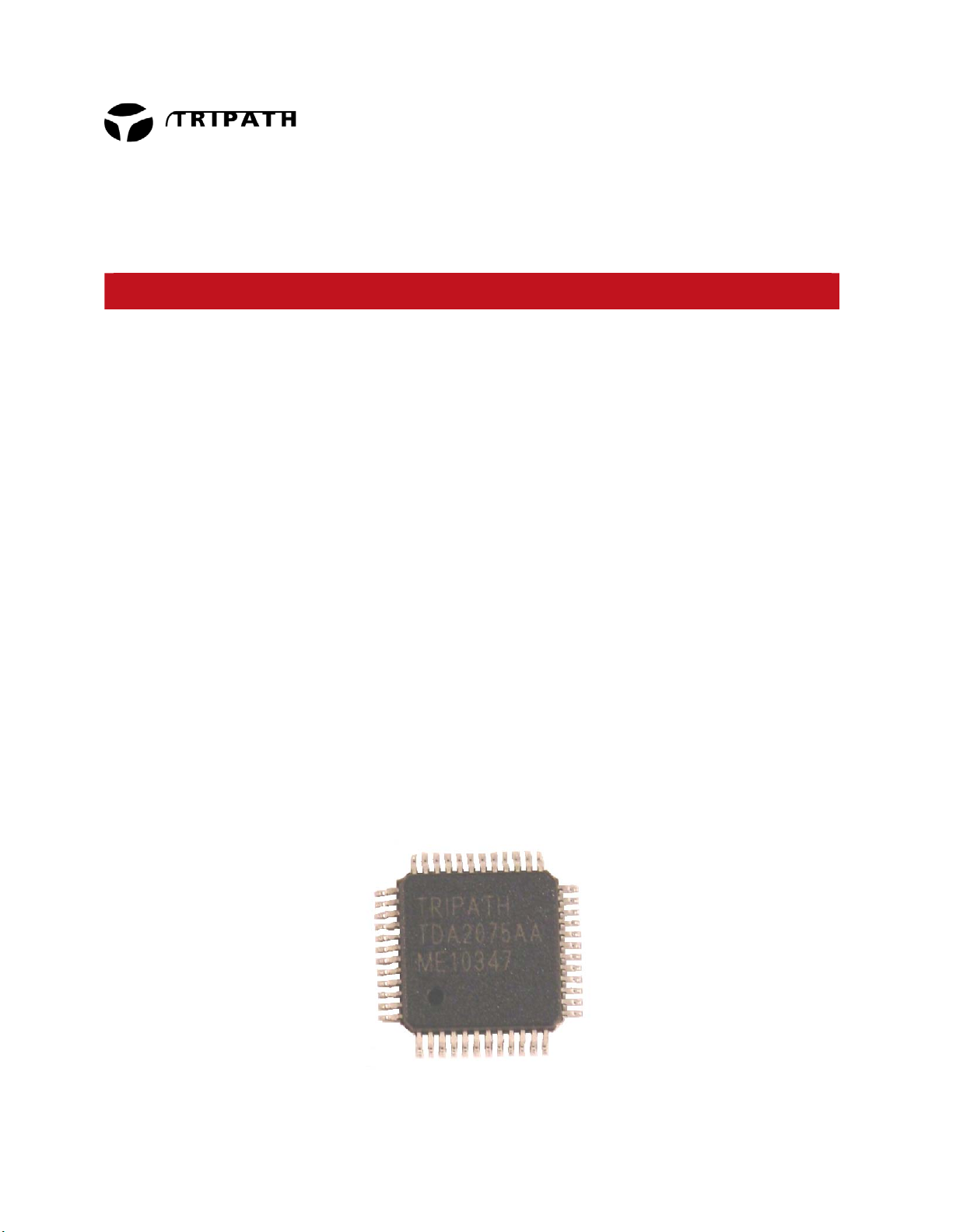
48-Pin LQFP Package
1 TDA2075A – Rev. 0.9/KLi/10.05
Page 2
Tripath Technology, Inc. - Technical Information
Absolute Maximum Ratings (Note 1)
SYMBOL PARAMETER Value UNITS
V5 5V Power Supply 6 V
V
Input logic level V5 + 0.3 V
logic
V10
T
STORE
VPP, VNN Supply Voltage (Note 5) +/-70 V
T
A
TJ Junction Temperature 150º °C
ESDHB
ESDMM ESD Susceptibility – Machine Model (Note 3)
10V Power Supply 12 V
Storage Temperature Range -55º to 150º °C
Operating Free-air Temperature Range -40º to 85º °C
ESD Susceptibility – Human Body Model (Note 2)
All pins
All pins
2000
200
V
V
Note 1: Absolute Maximum Ratings indicate limits beyond which damage to the device may occur.
See the table below for Operating Conditions.
Note 2: Human body model, 100pF discharged through a 1.5KΩ resistor.
Note 3: Machine model, 220pF – 240pF discharged through all pins.
Operating Conditions (Note 4)
SYMBOL PARAMETER MIN. TYP. MAX. UNITS
V5
V10 10V Power Supply 9 10 11 V
T
A
VPP Positive Supply Voltage (note 5) 15 65 V
VNN Negative Supply Voltage (note 5) -15 -65 V
Note 4: Recommended Operating Conditions indicate conditions for which the device is functional.
Note 5: The supply limitation is based on the internal over-current detection circuit. This limitation is
5V Power Supply 4.5 5 5.5 V
Operating Temperature Range -40 25 85 °C
See Electrical Characteristics for guaranteed specific performance limits.
subject to additional characterization. In addition, depending on feedback configuration, the TDA2075A
can be used in single-supply applications, in which case, the negative supply, VNN, is not needed.
Thermal Characteristics
SYMBOL PARAMETER Value UNITS
θ
JA
Junction-to-ambient Thermal Resistance (still air) TBD C/W
2 TDA2075A – Rev. 0.9/KLi/10.05
Page 3

Tripath Technology, Inc. - Technical Information
Electrical Characteristics TDA2075A (Note 6)
TA = 25 °C. See Application/Test Circuit on page 7. Unless otherwise noted, the supply voltages are
V5=5V, V10=10V, and VPP=|VNN|=40V.
SYMBOL PARAMETER CONDITIONS MIN. TYP. MAX. UNITS
I
5Q
I
10Q
I
VPPQ
I
VNNQ
I
5MUTE
V
TOC
I
VPPSENSE
V
VPPSENSE
I
VNNSENSE
V
VNNSENSE
Note 6: Minimum and maximum limits are guaranteed but may not be 100% tested.
Note 7: These supply voltages are calculated using the I
Quiescent Current
50 mA
(Mute = 0V)
Quiescent Current
(Mute = 0V)
Quiescent Current
(Mute = 0V)
Quiescent Current
(Mute = 0V)
Mute Supply Current
FETs: FQP13N10, FQP12P10
R
= 20.0kΩ
BBM
FETs: FQP13N10, FQP12P10
= 20.0kΩ
R
BBM
FETs: FQP13N10, FQP12P10
= 20.0kΩ
R
BBM
50
(Mute = 5V)
Over Current Sense Voltage
Threshold
+/-5V Common Mode Voltage
+/-40V Common Mode Voltage
VPPSENSE Threshold Currents Over-voltage turn on (muted)
Over-voltage turn off (mute off)
Under-voltage turn off (mute off)
Under-voltage turn on (muted)
Threshold Voltages with
= R
R
VPP1
VPP2
= 402KΩ
(Note 7)
Over-voltage turn on (muted)
Over-voltage turn off (mute off)
Under-voltage turn off (mute off)
Under-voltage turn on (muted)
VNNSENSE Threshold Currents Over-voltage turn on (muted)
Over-voltage turn off (mute off)
Under-voltage turn off (mute off)
Under-voltage turn on (muted)
Threshold Voltages with
= 402KΩ
R
VNN1
= 1.2MΩ
R
VNN2
(Note 7)
Over-voltage turn on (muted)
Over-voltage turn off (mute off)
Under-voltage turn off (mute off)
Under-voltage turn on (muted)
VPPSENSE
and I
Characteristics table. The typical voltage values shown are calculated using a R
60 mA
40 mA
40 mA
TBD
TBD
TBD
TBD
TBD
TBD
TBD
TBD
TBD
TBD
VNNSENSE
0.55
0.55
138
TBD
TBD
TBD
135
55
TBD
52
55.5
TBD
54.3
22.1
TBD
20.9
138
TBD
135
51
TBD
48
55.5
TBD
54.3
20.5
TBD
19.3
values shown in the Electrical
and R
VPP
mA
VNN
any tolerance variation. The minimum and maximum voltage limits shown include either a +1% or –1% (+1%
for Over-voltage turn on and Under-voltage turn off, -1% for Over-voltage turn off and Under-voltage turn on)
variation of R
VPP
or R
examples to show both typical and worst case voltage ranges for the given R
off the nominal 402kohm and 1.2Mohm values. These voltage specifications are
VNN
VPP
and R
VNN
Please refer to the Application Information section for a more detailed description of how to calculate the over
and under voltage trip voltages for a given resistor value.
V
A
µ
A
µ
A
µ
A
µ
V
V
V
V
A
µ
A
µ
A
µ
A
µ
V
V
V
V
values without
resistor values.
3 TDA2075A – Rev. 0.9/KLi/10.05
Page 4

Tripath Technology, Inc. - Technical Information
Performance Characteristics
TA = 25 °C. Unless otherwise noted, the supply voltages are V5 = 5V, V10 = 10V, and VPP = |VNN| =
40V, the input frequency is 1kHz and the measurement bandwidth is 20kHz. See Application/Test Circuit.
SYMBOL PARAMETER CONDITIONS MIN. TYP. MAX. UNITS
P
Output Power
OUT
(continuous output)
THD + N Total Harmonic Distortion Plus
Noise
IHF-IM IHF Intermodulation Distortion
SNR Signal-to-Noise Ratio
η
Power Efficiency
AV Amplifier Gain
THD+N = 0.1%, R
THD+N = 1%, R
THD+N = 10%, R
THD+N = 0.1%, R
THD+N = 1%, R
THD+N = 10%, R
THD+N = 0.1%, R
THD+N = 1%, R
THD+N = 10%, R
= 60W, RL = 8Ω
P
OUT
= 4Ω
L
= 4Ω
L
= 4Ω
L
= 6Ω
L
= 6Ω
L
= 6Ω
L
= 8Ω
L
= 8Ω
L
= 8Ω
L
19kHz, 20kHz, 1:1 (IHF), R
P
= 25W/Channel
OUT
A Weighted, R
= 200W/Channel
P
OUT
P
= 115W/Channel, RL = 8Ω
OUT
P
= 10W/Channel, RL = 8Ω
OUT
= 4Ω,
L
= 8Ω
L
0.01 %
0.03 %
104.4 dB
92 %
20.09 V/V
See Application / Test Circuit
A
Channel to Channel Gain Error
VERROR
P
= 10W/Channel, RL = 8Ω
OUT
See Application / Test Circuit
e
Output Noise Voltage A-Weighted, input shorted
NOUT
R
FBC
= 10kΩ, R
= 1.1kΩ, and R
FBB
FBA
170
= 1.0kΩ
V
Output Offset Voltage No Load, Mute = Logic Low
OFFSET
1% R
FBA, RFBB
and R
FBC
resistors
-1.0 1.0 V
145
160
200
105
115
150
80
90
115
W
W
W
W
W
W
W
W
W
0.5 dB
V
µ
4 TDA2075A – Rev. 0.9/KLi/10.05
Page 5
TDA2075A Pinout
Tripath Technology, Inc. - Technical Information
48-pin LQFP
(Top View)
NC
VNN SENSE
OVRLDB
VPPSENSE
AGND
AGND
OAOUT1
INV 1
MUTE
NC
OCD 1
OCD 2
REF
SUB
37
38
39
40
41
43
V5
44
V5
45
46
47
48
1
INV 2
DCMP
BIASCAP
OAOUT2
OCSP2
FAULT
NC
V5
30 29 27 2628 2536 35 33 3234 31
98765432
V5
AGND
BBMSET
GATEOFF
V10
FBOUT2
FBGND2
OCSN2
24
23
22
21
20
1942
18
17
16 NC
15
14
13
1110 12
OCSN1
OCSP1
FBGND1
FBOUT1
PGND
NC
HO2
NC
L02
NC
NC
LO1
HO1
NC
PGND
5 TDA2075A – Rev. 0.9/KLi/10.05
Page 6

Tripath Technology, Inc. - Technical Information
Pin Description
Pin Function Description
1 OAOUT2 Output of inverting-input stage (Channel 2)
2 INV2 Negative input of inverting op-amp with 2.5VDC of bias (Channel 2)
3 BIASCAP Bandgap reference times two (typically 2.5VDC). Used to set the common
mode voltage for the input op amps. This pin is not capable of driving external
circuitry.
4 DCMP Internal mode selection. This pin must be connected to 0V or 5V for proper
device operation. Typically, this pin is connected to V5.
5 AGND Analog Ground
6 V5 5 Volt power supply input.
7 BBMSET Break-before-make timing control to prevent shoot-through in the output
MOSFETs. Please refer to the Application Information for additional
information.
8 GATEOFF 10V under-voltage fault pin (requires pull-up resistor)
9, 10 OCSP1, OCSN1 Over-current detect pins (Channel 1)
11 FBKGND1 Ground Kelvin feedback (Channel 1)
12 FBKOUT1 Negative switching feedback (Channel 1)
13 PGND Power Ground
15 HO1 High side gate drive output (Channel 1)
17 L01 Low side gate drive output (Channel 1)
20 LO2 Low side gate drive output (Channel 2)
22 HO2 High side gate drive output (Channel 2)
24 PGND Power Ground
25 V10 10 Volt power supply input. Used for gate drive circuitry.
26 FBKGND2 Ground Kelvin feedback (Channel 2)
27 FBKOUT2 Negative switching feedback (Channel 2)
28, 29 OCSN2, OCSP2 Over-current detect pins (Channel 2)
30 FAULT A logic high output indicates an under-voltage (5V or 10V), over-current or
over-temperature condition (requires pull-down resistor).
32 V5 5 Volt power supply input.
33 OCD2 Over-Current Detect pin (Channel 2). This pin must be connected to AGND for
proper device operation.
34 REF Internal bandgap reference voltage; approximately 1.0 VDC.
35 OCD1 Over-Current Detect pin (Channel 1). This pin must be connected to AGND
for proper device operation.
36 SUB Substrate (connect to AGND)
38 VNNSENSE Negative supply voltage sense input. This pin is used for both over and under
voltage sensing for the VNN supply.
39 OVRLDB A logic low output indicates the input signal has overloaded the amplifier.
40 VPPSENSE Positive supply voltage sense input. This pin is used for both over and under
voltage sensing for the VPP supply.
41 AGND Analog Ground
42 AGND Analog Ground
43 V5 5 Volt power supply input.
44 V5 5 Volt power supply input.
45 OAOUT1 Output of inverting-input stage (Channel 1)
46 INV1 Negative input of inverting op-amp with 2.5VDC of bias (Channel 1)
47 MUTE When set to logic high, both channels are in idle mode. When low (grounded),
both channels are fully operational (connect to FAULT pin).
14,16,18,
19,21,23,
31,37,48
NC Not Connected internally. These pins may be grounded or left floating on the
PCB layout.
6 TDA2075A – Rev. 0.9/KLi/10.05
Page 7
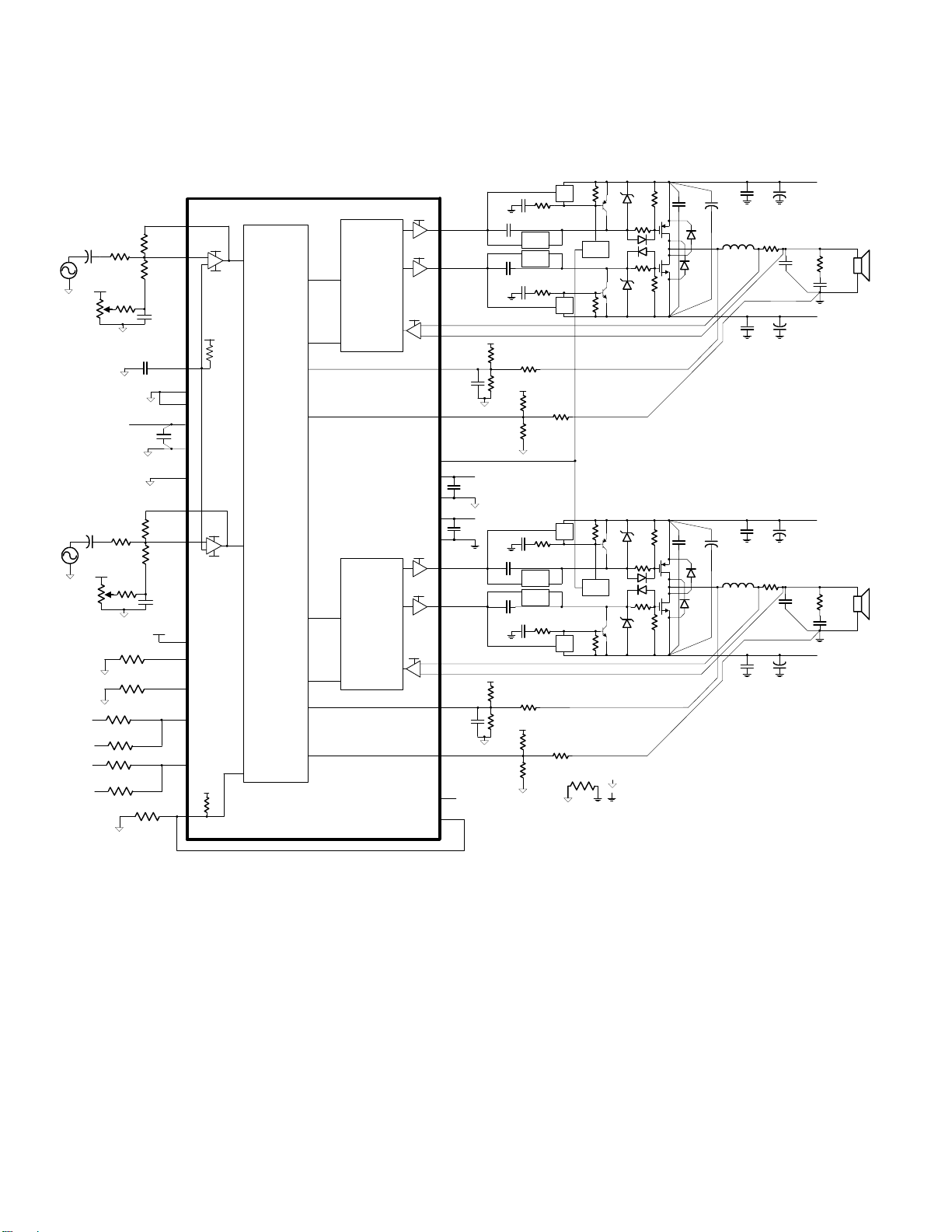
Application / Test Circuit
Tripath Technology, Inc. - Technical Information
C
2.2uF
R
50K
Offset Trim
Circuit
2.2uF
R
50K
Offset Trim
Circuit
VNN
VPP
**
TDA2075A
V5
V5
V10
V10
13,24
V10
V10
6, 32
15
HO1
LO1
17
OCSP1
9
OCSN1
10
FBKOUT1
12
FBKGND1
11
GATEOFF
8
V5
5
AGND
V10
25
PGND
22
HO2
20 LO2
OCSP2
29
OCSN2
28
FBKOUT2
27
FBKGND2
26
NC
FAULT
30
C
FB
150pF
C
FB
220pF
OAOUT1
45
I
R
R
I
F
20K
20K
+
V5
OFA
R
470K
R
OFB
470K
OFB
C
OF
0.1uF
AGND
C
A
0.1uF
BIASCAP
OCD2
OCD1
5V
C
S
0.1uF
AGND
OAOUT2
C
I
R
R
I
F
20K
20K
+
V5
OFA
V5
V5
R
470K
R
8.25K, 1%
R
*R
VNN1
*R
VNN2
*R
VPP1
*R
VPP2
OFB
AGND
REF
BBMSET
20K, 1%
R
OFB
470K
C
OF
V5
BBMSET
VNNSENSE
VPPSENSE
R
FLT
DCMP
MUTE
INV1
SUB
INV2
REF
V5
46
-
+
AGND
2.5V
FET controller
MUTE
3
33
35
V5
43, 44
41, 42
Processing
&
Modulation
36
1
V5
2
-
+
AGND
FET controller
4
34
7
MUTE
38
40
V5
14,16,18,19, 21, 23, 37, 48
47
10K
C
0.1uF
C
0.1uF
C
ISA
1.0uF
C
G
S_SUP
1.0uF
CKT
**
S_SUP
C
CKT
G
1.0uF
C
ISA
1.0uF
V5
R
*R
FBA
FBC
1K
10K, 1%
*R
FBB
V5
1.1K
R
1K
*R
5V
S
10V
S
C
ISA
1.0uF
C
G
S_SUP
1.0uF
CKT
**
S_SUP
C
CKT
G
1.0uF
C
ISA
1.0uF
V5
R
*R
FBA
FBC
1K
10K, 1%
*R
FBB
1.1K
V5
R
1K
*R
R
D_IS
ISA
D
BIAS
Q
ISP
D
BIAS
Q
ISN
D
BIAS
Q
ISP
D
BIAS
Q
ISN
Analog Ground
R
GS
C
150K
R
G
D
G
D
G
R
G
R
GS
150K
R
GS
150K
R
G
D
G
D
G
R
G
R
GS
150K
HBR
0.1uF
Q
P
D
Q
N
D
DS
C
HBR
0.1uF
Q
P
D
Q
N
D
DS
1.1K
1.1K
R
1.0K
R
1.0K
FBA
FBB
R
1.0K
R
1.0K
FBA
FBB
ISB
ISB
*R
10K, 1%
ISB
ISB
*R
10K, 1%
CKT
**
D_IS
CKT
FBC
**
D_IS
CKT
**
D_IS
CKT
FBC
4.7K
**
G_OFF
R
ISA
4.7K
R
ISA
4.7K
**
G_OFF
R
ISA
4.7K
Ω
0
CKT
CKT
Power Ground
* The values of these components must be adjusted based
on supply volt age range. See Applic ation Information.
** Refer to the RB- TDA2075A docume nt for a detailed
description of these optional circuits.
C
S
0.1uF
C
+
HBR
33uF
L
O
DS
11uH
R
S
C
S
0.1uF
C
S
0.1uF
C
+
HBR
33uF
L
L
O
O
DS
11uH
R
S
C
S
0.1uF
VPP
C
+
S
220uF
R
C
O
Z
R
0.22uF
10Ω,2W
C
Z
0.22uF
VNN
C
S
+
220uF
VPP
C
+
S
220uF
R
C
O
Z
0.22uF
10Ω,2W
C
Z
0.22uF
VNN
C
S
+
220uF
L
4 - 8Ω
R
L
4 - 8Ω
7 TDA2075A – Rev. 0.9/KLi/10.05
Page 8

Tripath Technology, Inc. - Technical Information
External Components Description (Refer to the Application/Test Circuit)
Components Description
R
Inverting input resistance to provide AC gain in conjunction with RF. This input is
I
RF Feedback resistor to set AC gain in conjunction with RI. Please refer to the Amplifier
CI AC input coupling capacitor which, in conjunction with RI, forms a high-pass filter at
R
Feedback divider resistor connected to V5. This value of this resistor depends on
FBA
R
Feedback divider resistor connected to AGND. This value of this resistor depends
FBB
R
Feedback resistor connected from either the OUT1 (OUT2) to FBKOUT1
FBC
CFB Feedback delay capacitor that both lowers the idle switching frequency and filters
R
Potentiometer used to manually trim the DC offset on the output of the TDA2075A.
OFA
R
Resistor that limits the DC offset trim range and allows for precise adjustment.
OFB
COF Capacitor that filters the manual DC offset trim voltage.
R
Bias resistor. Locate close to pin 34 and ground to plane with a low impedance
REF
R
Bias current setting resistor for the BBM setting. Locate close to pin 7 and ground
BBMSET
CA BIASCAP decoupling capacitor. Locate close to pin 3 and ground to plane with a
CS Supply decoupling capacitor for the power pins. For optimum performance, these
R
Main overvoltage and undervoltage sense resistor for the negative supply (VNN).
VNN1
R
Secondary overvoltage and undervoltage sense resistor for the negative supply
VNN2
R
Main overvoltage and undervoltage sense resistor for the positive supply (VPP).
VPP1
R
Secondary overvoltage and undervoltage sense resistor for the positive supply
VPP2
biased at the BIASCAP voltage (approximately 2.5VDC).
Gain paragraph, in the Application Information section.
.
)CR2(1f
π=
IIC
the supply voltage setting and helps set the TDA2075A gain in conjunction with R
R
F, RFBA,
and R
. Please see the Modulator Feedback Design paragraphs in the
FBC
I,
Application Information Section.
on the supply voltage setting and helps set the TDA2075A gain in conjunction with
R
I, RF, RFBA,
and R
. Please see the Modulator Feedback Design paragraphs in
FBC
the Application Information Section.
(FBKOUT2) or PGND1 (PGND2) to FBKGND1 (FBKGND2). The value of this
resistor depends on the supply voltage setting and helps set the TDA2075A gain in
conjunction with R
I, RF, RFBA,
power rating of greater than
, and R
=
DISS
. It should be noted that R
FBB
2
. Please see the Modulator
)(2RVPPP FBC
must have a
FBC
Feedback Design paragraphs in the Application Information Section.
very high frequency noise from the feedback signal, which improves amplifier
performance. The value of C
should be different for channel 1 and channel 2 to
FB
minimize noise coupling between the channels. Please refer to the Application /
Test Circuit.
connection to pins 41 and 42.
directly to pin 5. See Application Information on how to determine the value for
R
.
BBM
low impedance connection to pins 41 and 42.
components should be located close to the TDA2075A and returned to their
respective ground as shown in the Application Circuit.
Please refer to the Electrical Characteristics Section for the trip points as well as the
hysteresis band. Also, please refer to the Over / Under-voltage Protection section in
the Application Information for a detailed discussion of the internal circuit operation
and external component selection. When using a single power supply, this circuit
can be defeated by connecting a 16KΩ resistor to AGND.
(VNN). This resistor accounts for the internal V
resistor value should be three times that of R
VNN1
NNSENSE
bias of 1.25V. Nominal
. Please refer to the Over / Undervoltage Protection section in the Application Information for a detailed discussion of
the internal circuit operation and external component selection. When using a single
power supply, omit R
VNN2
.
Please refer to the Electrical Characteristics Section for the trip points as well as the
hysteresis band. Also, please refer to the Over / Under-voltage Protection section in
the Application Information for a detailed discussion of the internal circuit operation
and external component selection.
8 TDA2075A – Rev. 0.9/KLi/10.05
Page 9

Tripath Technology, Inc. - Technical Information
(VPP). This resistor accounts for the internal V
resistor value should be equal to that of R
VPP1
PPSENSE
. Please refer to the Over / Under-
bias of 2.5V. Nominal
voltage Protection section in the Application Information for a detailed discussion of
the internal circuit operation and external component selection.
RS Over-current sense resistor. Please refer to the section, Setting the Over-current
Threshold, in the Application Information for a discussion of how to choose the value
of R
to obtain a specific current limit trip point.
S
C
Supply decoupling for the high current Half-bridge supply pins. These components
HBR
must be located as close to the output MOSFETs as possible to minimize output
ringing which causes power supply overshoot. By reducing overshoot, these
capacitors maximize both the TDA2075A and output MOSFET reliability. These
capacitors should have good high frequency performance including low ESR and
low ESL. In addition, the capacitor rating must be twice the maximum VPP voltage.
Panasonic EB capacitors are ideal for the bulk storage (nominally 33uF) due to their
high ripple current and high frequency design.
RG Gate resistor, which is used to control the MOSFET rise/ fall times. This resistor
serves to dampen the parasitics at the MOSFET gates, which, in turn, minimizes
ringing and output overshoots. The typical power rating is 1/2 watt.
DG Gate diode, which adds additional BBM and serves to match the unequal rise and
fall times of Q
and QP. An ultra-fast diode with a current rating of at least 200mA
N
should be used.
D
Diode that keeps the gate capacitor biased at the proper voltage when the supply
BIAS
voltage decreases.
CG Gate capacitor that ac-couples the TDA2075A from the high voltage MOSFETs.
R
ISA, RISB
C
ISA
Q
ISP
Q
ISN
Bias resistors for the increasing supply circuits.
Bias capacitor for the increasing supply circuits.
P-channel bipolar transistor for the circuit which charges the high side gate
capacitors, C
to VPP, in the case where the VPP supply increases in magnitude.
G,
N-channel bipolar transistor for the circuit which charges the low side gate
capacitors, C
to VNN, in the case where the VNN supply increases in magnitude.
G,
CZ Zobel capacitor, which in conjunction with RZ, terminates the output filter at high
frequencies. Use a high quality film capacitor capable of sustaining the ripple current
caused by the switching outputs.
QP P-channel power-MOSFET of the output stage.
QN N-channel power-MOSFET of the output stage.
RZ Zobel resistor, which in conjunction with CZ, terminates the output filter at high
frequencies. The combination of R
and CZ minimizes peaking of the output filter
Z
under both no load conditions or with real world loads, including loudspeakers which
usually exhibit a rising impedance with increasing frequency. Depending on the
program material, the power rating of R
may need to be adjusted. The typical
Z
power rating is 2 watts.
LO Output inductor, which in conjunction with CO, demodulates (filters) the switching
waveform into an audio signal. Forms a second order filter with a cutoff frequency
of
C
O
D
DS
Output capacitor, which, in conjunction with L
waveform into an audio signal. Forms a second order low-pass filter with a cutoff
frequency of
Use a high quality film capacitor capable of sustaining the ripple current caused by
the switching outputs.
These diodes must be connected from either the drain of the p-channel MOSFET to
the source of the n-channel MOSFET, or the source of the p-channel MOSFET to
the drain of the n-channel MOSFET. This diode absorbs any high frequency
overshoots caused by the output inductor L
In order for this diode to be effective it must be connected directly to the two
π=
and a quality factor of
)CL2(1f
OOC
and a quality factor of
π=
)CL2(1f
OOC
.
CLCRQ =
OOOL
, demodulates (filters) the switching
O
CRQ CL2
=
during high output current conditions.
O
OOL
O
MOSFETs. An ultra-fast recovery diode that can sustain the entire supply voltage
should be used here. In most applications a 100V or greater diode must be used.
RGS Resistor that turns QN and QP off when no signal is present.
R
Pull-down resistor for the open-drain Fault circuit.
FLT
.
9 TDA2075A – Rev. 0.9/KLi/10.05
Page 10

Typical Performance Characteristics
10
RL = 4 Ω
V PP = |V NN| = 30V, 35V and 40V
f = 1kHz
BW = 22Hz - 20kHz(A ES17)
1
%
0.1
THD +N ve rsus Output P ower
Tripath Technology, Inc. - Technical Information
10
RL = 4Ω
Pout = 25W / Channel
VPP = |VNN| = 40V
BW = 22Hz-22kHz
0.1
%
THD+N versus Freque ncy
0.01
0.001
1 2002 5 10 20 50 100
W
10
RL = 6 Ω
VPP = |VNN| = 30V, 35V and 40V
f = 1kHz
BW = 22Hz - 20kHz(A ES17)
1
%
0.1
0.01
0.001
1 2002 5 10 20 50 100
THD +N ve rsus Outp ut P o we r
W
10
RL = 8Ω
VPP = |VNN| = 30V, 35V and 40V
f = 1kHz
BW = 22Hz - 20kHz(A ES17)
1
THD +N versus Outp ut P o we r
300
300
0.01
0.001
10 20k50 100 200 500 1k 2k 5k 10k
20
Hz
10
RL = 6Ω
Pout = 25W / Channel
V PP = | V NN| = 4 0 V
BW = 22 Hz - 22 kHz
0.1
%
0.01
0.001
10
20
THD+N versus Freque ncy
Hz
20k50 100 200 500 1k 2k 5k 10k
10
RL = 8Ω
Pout = 25W / Channel
VPP = |VNN| = 40V
BW = 22Hz-22kHz
0.1
THD+N versus Freque ncy
%
0.1
0.01
0.001
1 2002 5 10 20 50 100
W
300
%
0.01
0.001
10
20
Hz
10 TDA2075A – Rev. 0.9/KLi/10.05
20k50 100 200 500 1k 2k 5k 10k
Page 11

Typical Performance Characteristics
Efficiency and Power Dissipation versus
90
80
70
60
50
40
Effici ency (%)
30
20
10
0
Efficiency
0 25 50 75 100 125
Output Power
Pow er Diss ipation
Output Power per channel
(W)
VPP = |VNN| = 40V
R
= 4Ω
L
f= 1kHz
BW = 22Hz - 20kHz(AES17)
150
175 200 225
Tripath Technology, Inc. - Technical Information
+0
45
40
35
30
25
(W)
20
15
10
Power Dissipation pe r channel
5
0
RL = 8Ω
19kHz, 20kHz, 1:1
-20
0dBr = 12Vrms
FFT si z e = 3 2k
FFT
-40
VPP = |VNN| = 40V
d
BW = 22Hz - 80kHz
-60
B
r
-80
A
-100
-120
-140
20 30k50 100 200 500 1k 2k 5k 10k
Intermodulation Performance
= 65kHz
SR
Hz
Efficiency and Power Dissipation versus
90
80
70
60
50
40
Efficiency (%)
30
20
10
0
Efficiency
0 25 50 75 100 125
Output Power
Power Dissipation
Output Power per channel
(W)
VPP = |VNN| = 40V
= 6Ω
R
L
f= 1kHz
BW = 22Hz - 20kHz(AES17)
150
Efficiency and Power Dissipation versus
100
90
80
70
60
50
40
Efficiency (%)
30
20
10
0
0255075100125
Efficiency
Output Power
Power Dissipation
Output Power per channel
(W)
VPP = |VNN| = 40V
R
= 8Ω
L
f= 1kHz
BW = 22Hz - 20kHz(AES17)
175
-70
20100
18
16
14
12
10
(W)
8
6
4
Power Dissipation per channel
2
0
VPP = |VNN| = 40V
FFT size = 32k
FFT
= 48kHz
SR
BW = 22Hz-20kHz(A ES17)
-80
-90
d
B
V
-100
-110
-120
20 20k50 10 0 200 500 1k 2k 5k 10k
Noise Floor
Hz
Channel Separation versus Frequency
TTT
+0
20
18
16
14
12
10
(W)
8
6
4
Power Dissipation per channel
2
0
0dBr = 12Vr ms
VPP = |VNN| = 40V
BW = 22Hz - 20kHz
-20
-40
d
B
r
-60
A
-80
-100
20 20k50 100 200
1k 2k 5k 10k
500
Hz
11 TDA2075A – Rev. 0.9/KLi/10.05
Page 12

Tripath Technology, Inc. - Technical Information
Application Information
Figure 1 is a simplified diagram of one channel (Channel 1) of a TDA2075A amplifier to assist in
understanding its operation.
TDA2075A
OCSN1
Offset Trim
Circuit
VNN
VPP
V5
V5
OVER
OAOUT1
45
R
R
C
I
+
R
OFA
R
VNN1
R
VPP1
R
VNN2
R
VPP2
F
I
R
OFB
V5
C
C
A
BIASCAP
R
REF
VNNSENSE
VPPSENSE
5V
C
S
AGND
INV1
OF
V5
46
AGND
3
34REF
38
40
32,43,44
41,42
V5
-
+
2.5V
Processing
Modulation
OVER/
UNDER
VOLTAGE
DETECTION
&
12
FBKOUT1
11 FBKGND1
CURRENT
DETECTION
IN1Y1B
CONTROLLER
C
FB
FET
R
10
OCSP1
9
V10
V10
25
13,24
V5
R
R
FBA
R
FBB
FBB
C
R
G
15
HO1
LO1
17
V10
PGND
V5
6
5
AGND
FBA
R
FBC
R
G
C
R
G
G
10V
C
S
5V
C
S
FBC
C
S
Q
P
C
HBR
Q
N
VPP
R
OUTPUT
FILTER
VNN
C
S
S
R
L
Analog Ground
Power Ground
Figure 1: Simplified TDA2075A Amplifier
TDA2075A Basic Amplifier Operation
The audio input signal is fed to the processor internal to the TDA2075A, where a switching pattern is
generated. The average idle (no input) switching frequency is approximately 700kHz. With an input
signal, the pattern is spread spectrum and varies between approximately 200kHz and 1.5MHz depending
on input signal level and frequency. These switching patterns are inputted to a MOSFET driver and then
outputted to HO1 and LO1 which are ac-coupled to a complementary pair of power MOSFETs. The
output of the MOSFETs is a power-amplified version of the switching pattern that switches between VPP
and VNN. This signal is then low-pass filtered to obtain an amplified reproduction of the audio input
signal.
The processor is operated from a 5-volt supply while the FET driver is operated from a 10-volt supply.
The FET driver inserts a “break-before-make” dead time between the turn-off of one transistor and the
turn-on of the other in order to minimize shoot-through currents in the external MOSFETs. The dead time
can be programmed by adjusting R
BBMSET. Feedback information from the output of the complementary
FETs is supplied to the processor via FBKOUT1. Additional feedback information to account for ground
bounce is supplied via FBKGND1.
Complementary MOSFETs are used to formulate a half-bridge configuration for the power stage of the
amplifier. The gate capacitors, C
MOSFETs. The gate resistors, R
, are used to ac-couple the FET driver to the complementary
G
, are used to control MOSFET slew rate and thereby minimize voltage
G
overshoots.
12 TDA2075A – Rev. 0.9/KLi/10.05
Page 13

Tripath Technology, Inc. - Technical Information
Circuit Board Layout
The TDA2075A is a power (high current) amplifier that operates at relatively high switching frequencies.
The output of the amplifier switches between VPP and VNN at high speeds while driving large currents.
This high-frequency digital signal is passed through an LC low-pass filter to recover the amplified audio
signal. Since the amplifier must drive the inductive LC output filter and speaker loads, the amplifier
outputs can be pulled above the supply voltage and below ground by the energy in the output inductance.
To avoid subjecting the TDA2075A and the complementary MOSFETs to potentially damaging voltage
stress, it is critical to have a good printed circuit board layout. It is recommended that Tripath’s layout and
application circuit be used for all applications and only be deviated from after careful analysis of the
effects of any changes. Please refer to the TDA2075A reference board document, RB-TDA2075A,
available on the Tripath website, at www.tripath.com.
The trace that connects the drain of the p-channel output MOSFET to the drain of the n-channel output
MOSFET is very important. This connection should be as wide and short as possible. A jumper wire of
16 gauge or more can be used in parallel with the trace to reduce any trace resistance or inductance.
Any resistance or inductance on this trace can cause the switching output to over/undershoot potentially
causing damage to both the TDA2075A and the output MOSFETs.
The following components are important to place near the TDA2075A or output MOSFET pins. The
recommendations are ranked in order of layout importance, either for proper device operation or
performance considerations.
- The capacitors, C
provide high frequency bypassing of the amplifier power supplies and will
HBR,
serve to reduce spikes across the supply rails. Please note that both MOSFET half-bridges
must be decoupled separately. In addition, the voltage rating for C
should be at least 150V
HBR
as this capacitor is exposed to the full supply range, VPP-VNN.
- C
removes very high frequency components from the amplifier feedback signals and lowers
FB
the output switching frequency by delaying the feedback signals. In addition, the value of C
FB
is
different for channel 1 and channel 2 to keep the average switching frequency difference
greater than 40kHz. This minimizes in-band audio noise. The capacitors, C
, should be
FB
surface mount types, located on the “solder” side of the board as close to their respective
TDA2075A pins as possible.
- D
should be placed as close to the drain and source of the output MOSFETs as possible with
DS
direct routing either from the drain of the p-channel MOSFET to the source of the n-channel
MOSFET or from the source of the p-channel MOSFET to the drain of the n-channel MOSFET.
The output over/undershoots are very high-speed transients. If these diodes are placed too far
away from the MOSFETs, they will be ineffective.
- To minimize noise pickup and minimize THD+N, R
FBA
, R
FBB
, and R
should be located as
FBC
close to the TDA2075A as possible. Make sure that the routing of the high voltage feedback
lines is kept far away from the input op amps or significant noise coupling may occur. It is best
to shield the high voltage feedback lines by using a ground plane around these traces as well
as the input section. The feedback and feedback ground traces should be routed together in
parallel.
- The main supply decoupling capacitors, C
and Q
capacitors, C
. These will absorb energy when DSD and DDS conduct. Also, the bulk decoupling
P
, will shunt energy generated by the main supply lead trace inductance.
S
, should be located close to the output devices, QN
S
Some components are not sensitive to location but are very sensitive to layout and trace routing.
- For proper over-current detection, the sense lines connected to R
directly from the terminals of R
back to OCSP1 (OCSP2) and OCSN1 (OCSN2). The traces
S
must be kelvin connected
S
should be run in parallel back to the TDA2075A pins without deviation. Improper layout with
respect to R
will result in premature over-current detection due to additional IR losses.
S
13 TDA2075A – Rev. 0.9/KLi/10.05
Page 14

Tripath Technology, Inc. - Technical Information
- To maximize the damping factor and reduce distortion and noise, the modulator feedback
connections should be routed directly to the pins of the output inductors. L
.
O
- The output filter capacitor, C
, and zobel capacitor, CZ, should be star connected with the load
O
return. The output ground feedback signal should be taken from this star point.
- The modulator feedback resistors, R
FBA
and R
, should all be grounded and attached to 5V
FBB
together. These connections will serve to minimize common mode noise via the differential
feedback.
- The feedback signals that come directly from the output inductors are high voltage and high
frequency in nature. If they are routed close to the input nodes, INV1 and INV2, the high
impedance inverting op-amp pins will pick up noise. This coupling will result in significant
background noise, especially when the input is AC coupled to ground, or an external source
such as a CD player or signal generator is connected. Thus, care should be taken such that
the feedback lines are not routed near any of the input section.
- To minimize the possibility of any noise pickup, the trace lengths of INV1 and INV2 should be
kept as short as possible. This is most easily accomplished by locating the input resistors, R
and the input stage feedback resistors, R
the offset trim resistor, R
, which connects to either INV1, or INV2, should be located close to
OFB
as close to the TDA2075A as possible. In addition,
F
I
the TDA2075A input section.
TDA2075A Grounding
Proper grounding techniques are required to maximize TDA2075A functionality and performance.
Parametric parameters such as THD+N, Noise Floor and Crosstalk can be adversely affected if proper
grounding techniques are not implemented on the PCB layout. The following discussion highlights some
recommendations about grounding both with respect to the TDA2075A as well as general “audio system”
design rules.
The TDA2075A is divided into three sections: the input processor section, the FET driver section, and the
complementary output MOSFETs (high voltage) section. On the TDA2075A evaluation board, the ground
is also divided into distinct sections, Analog Ground (AGND) and Power Ground (PGND). To minimize
ground loops and keep the audio noise floor as low as possible, the two grounds must be only connected
at a single point.
The ground for the 5V supply is referred to as the analog ground and must be connected to pins 5, 41,
and 42 on the TDA2075A. Additionally, any external input circuitry such as preamps, or active filters,
should be referenced to the analog ground. The substrate, pin 36, should also be connected to the
analog ground.
For the power section, Tripath has traditionally used a “star” grounding scheme. Thus, the load ground
returns and the power supply decoupling traces are routed separately back to the power supply. In
addition, any type of shield or chassis connection would be connected directly to the ground star located
at the power supply. These precautions will both minimize audible noise and enhance the crosstalk
performance of the TDA2075A. It is possible to use a low impedance ground plane for PGND as well.
But the ground plane must be contiguous or ground currents from each channel can create crosstalk
issues. To minimize these issues, the FBKOUT1 (FBKOUT2) lines should be routed directly from the
PGND side of the load.
The TDA2075A incorporates a differential feedback system to minimize the effects of ground bounce and
cancel out common mode ground noise. Therefore, the feedback from the output ground for each
channel needs to be properly sensed. This can be accomplished by connecting the output ground
“sensing” trace directly to the star formed by the output ground return, output capacitor, C
capacitor, C
. Refer to the Application / Test Circuit for a schematic description.
Z
, and the zobel
O
14 TDA2075A – Rev. 0.9/KLi/10.05
Page 15

Tripath Technology, Inc. - Technical Information
TDA2075A Amplifier Gain
The gain of the TDA2075A is the product of the input stage gain and the modulator gain for the
TDA2075A. Please refer to the sections, Input Stage Design, and Modulator Feedback Design, for a
complete explanation of how to determine the external component values.
TDA2075A
V
INPUTSTAGE
V
MODULATOR
A*A A =
V
R
F
TDA2075A
A
V
−≈ 1
R
I
+
FBBFBAFBC
R*R
FBBFBA
)R(R*R
+
For example, using a TDA2075A with the following external components,
R
R
R
= 20kΩ
I
= 20kΩ
R
F
= 1kΩ
R
FBA
= 1.1kΩ
FBB
= 10.0kΩ
FBC
A
TDA2075A
V
−≈
20k Ω
20k Ω
1.1k Ω*1.0k Ω
)1.1k(1.0k Ω*10.0k Ω
Ω+
20.09- 1
=
+
V
V
Input Stage Design
The TDA2075A input stage is configured as an inverting amplifier, allowing the system designer flexibility
in setting the input stage gain and frequency response. Figure 2 shows a typical application where the
input stage is a constant gain inverting amplifier. The input stage gain should be set so that the maximum
input signal level will drive the input stage output to 4Vpp.
The gain of the input stage, above the low frequency high pass filter point, is that of a simple inverting
amplifier:
R
F
A −=
EVINPUTSTAG
I
R
TDA2075A
OAOUT1
INPUT1
INPUT2
45
C
R
I
+
C
I
+
R
I
F
R
I
R
F
INV1
INV2
OAOUT2
46
BIASCAP
1
2
V5
-
+
AGND
V5
+
-
AGND
Figure 2: TDA2075A Input Stage
15 TDA2075A – Rev. 0.9/KLi/10.05
Page 16

Tripath Technology, Inc. - Technical Information
Input Capacitor Selection
C
can be calculated once a value for RI has been determined. CI and RI determine the input low-
I
frequency pole. Typically this pole is set below 10Hz to minimize attenuation at 20Hz. C
is calculated
IN
according to:
C
= 1 / (2π x FP x RI)
I
where: R
= Input resistor value in ohms (typically 20kΩ)
I
F
= Input low frequency pole (typically 3.6Hz)
P
Modulator Feedback Design
The modulator converts the signal from the input stage to the high-voltage output signal. The optimum
gain of the modulator is determined from the maximum allowable feedback level for the modulator and
maximum supply voltages for the power stage. Depending on the maximum supply voltage, the feedback
ratio will need to be adjusted to maximize performance. The values of R
FBA
, R
FBB
and R
FBC
(see
explanation below) define the gain of the modulator. Once these values are chosen, based on the
maximum supply voltage, the gain of the modulator will be fixed.
For the best signal-to-noise ratio and lowest distortion, the maximum modulator feedback voltage should
be approximately 4Vpp. The modulator feedback resistor R
should be adjusted so that the modulator
FBC
feedback voltage is approximately 4Vpp. This will keep the gain of the modulator as low as possible and
still allow headroom so that the feedback signal does not clip the modulator feedback stage. Increasing
the value of R
will increase the modulator gain. Sometimes increasing the value of R
FBC
may be
FBC
necessary to achieve full power for the amplifier since the input stage will clip at approximately 4Vpp. This
will ensure that the input stage doesn’t clip before the output stage.
Figure 3 shows how the feedback from the output of the amplifier is returned to the input of the modulator.
The input to the modulator (FBKOUT1/FBKGND1 for channel 1) can be viewed as inputs to an inverting
differential amplifier. R
FBA
and R
bias the feedback signal to approximately 2.5V and R
FBB
scales the
FBC
large OUT1/OUT2 signal to down to 4Vpp.
1/2 TDA2075A
V5
Processing
&
Modulation
FBKOUT1
FBKGND1
R
FBA
R
FBB
AGND
R
FBA
R
FBC
OUT1
R
R
FBB
OUT1 GROUND
FBC
Figure 3: Modulator Feedback
16 TDA2075A – Rev. 0.9/KLi/10.05
Page 17

For SPLIT-SUPPLY operation:
Ω
+
Ω
Ω
+
Ω
The modulator feedback resistors are:
R
= 1Ktypically specified, UserRFBA
VPP*R
FBA
FBB
=
4)-(VPP
R
FBA
FBC
=
VPP*R
4
FBBFBAFBC
)R(R*R
A
MODULATOR-V
≈
FBBFBA
R*R
1
+
The above equations assume that VPP=|VNN|.
For example, in a system with a SPLIT-SUPPLY of VPP
MAX
R
R
R
= 1kΩ, 1%
FBA
= 1.111kΩ, use 1.1kΩ, 1%
FBB
= 10.0kΩ, use 10.0kΩ, 1%
FBC
The resultant modulator gain is:
A MODULATOR-V =+
≈
+
)1.1k(1.0k Ω*10.0k Ω
20.09V/V 1
1.1k Ω*1.0k Ω
For SINGLE-SUPPLY operation:
The modulator feedback resistors are:
= 1K typicallyspecified,User R FBB
1000*350R FBC −= VPP
R* 2333.33
FBC
R
A
FBB
=
+
MODULATOR-V
≈
FBC
)R(1000
)R(R*R
FBBFBAFBC
R*R
FBBFBA
1
+
For example, in a system with a SINGLE-SUPPLY of VPP
R
R
R
= 2.17kΩ, use 2.15kΩ, 1%
FBA
= 1kΩ, 1%
FBB
= 13.0kΩ, use 13.0kΩ, 1%
FBC
The resultant modulator gain is:
A MODULATOR-V =+
≈
+
)2.15k(1.0k Ω*13.0k Ω
20.05V/V 1
2.15k Ω*1.0k Ω
Tripath Technology, Inc. - Technical Information
=40V and VNN
MAX
=-40V,
= 40V,
MAX
17 TDA2075A – Rev. 0.9/KLi/10.05
Page 18

Tripath Technology, Inc. - Technical Information
DC Offset
While the DC offset voltages that appear at the speaker terminals of a TDA2075A amplifier are typically
small, Tripath recommends that all offsets be removed with the circuit shown in Figure 4. It should be
noted that the DC voltage on the output of a muted TDA2075A with no load is approximately 2.5V. This
offset does not need to be nulled. The output impedance of the amplifier in mute mode is approximately
10KΩ thus explaining why the DC voltage drops to essentially zero when a typical load is connected.
2.2uF, 25V
+
C
I
V5
10kΩ
20.0kΩ
R
I
470k
Input to TDA2075A
(DC Bias ~2.5V)
Ω
470k
Ω
0.1uF, 50V
Figure 4: Offset Adjustment
Mute
When a logic high signal is supplied to MUTE, both amplifier channels are muted (complementary
MOSFETs are turned off). When a logic level low is supplied to MUTE, both amplifiers are fully
operational. There is a delay of approximately 240 milliseconds between the de-assertion of MUTE and
the un-muting of the TDA2075A.
Turn-on & Turn-off Noise
If turn-on or turn-off noise is present in a TDA2075A amplifier, the cause is frequently due to other
circuitry external to the TDA2075A. The TDA2075A has additional circuitry, as compared to previous
Tripath amplifiers, which virtually eliminate any transients during power up and power down. While the
TDA2075A has sophisticated circuitry to suppress turn-on and turn-off transients, the combination of the
power supply and other audio circuitry with the TDA2075A in a particular application may exhibit audible
transients. It is recommended that MUTE is active (pulled high) during power up and power down to
minimize any audible transients caused by audio circuitry that precedes the TDA2075A.
Over-current Protection
The TDA2075A has over-current protection circuitry to protect itself and the output transistors from shortcircuit conditions. The TDA2075A senses the voltage across resistor R
condition. Resistor R
is in series with the load just after the low pass filter. The voltage is measured via
S
to detect an over-current
S
OCSP1 and OCSN1 for channel 1 and OCSP2 and OCSN2 for channel 2. The OCS* pins must be Kelvin
connected for proper operation. See “Circuit Board Layout” in Application Information for details.
When the voltage across R
becomes greater than V
S
(typically 0.5V), the TDA2075A will shut off the
TOC
output stages of its amplifiers. The occurrence of an over-current condition also causes the TDA2075A
Fault pin (pin 30) to go high. It is recommended that the Fault pin be connected externally to the mute pin
to mute the processor during an over-current condition. The Fault circuitry is an open drain configuration
and requires a pull-down resistor. The removal of the over-current condition returns the amplifier to
normal operation.
18 TDA2075A – Rev. 0.9/KLi/10.05
Page 19

Tripath Technology, Inc. - Technical Information
Setting Over-current Threshold
R
determines the value of the over-current threshold, ISC:
S
I
= V
SC
V
= Over-current sense threshold voltage (See Electrical Characteristics Table)
TOC
where RS is in Ω’s
TOC/RS
= 0.55V typically
For example, to set an I
of 11A, RS will be 50mΩ.
SC
Over- and Under-Voltage Protection
The TDA2075A senses the power rails through external resistor networks connected to VNNSENSE and
VPPSENSE. The over- and under-voltage limits are determined by the values of the resistors in the
networks, as described in the table “Test/Application Circuit Component Values”. If the supply voltage
falls outside the upper and lower limits determined by the resistor networks, the TDA2075A shuts off the
output stages of the amplifiers. The removal of the over-voltage or under-voltage condition returns the
TDA2075A to normal operation. Please note that trip points specified in the Electrical Characteristics
table are at 25°C and may change over temperature.
The TDA2075A has built-in over and under voltage protection for both the VPP and VNN supply rails.
The nominal operating voltage will typically be chosen as the supply “center point.” This allows the
supply voltage to fluctuate, both above and below, the nominal supply voltage.
VPPSENSE (pin 40) performs the over and undervoltage sensing for the positive supply, VPP.
VNNSENSE (pin 38) performs the same function for the negative supply, VNN. When the current through
VPPSENSE (or VNNSENSE) goes below or above the values shown in the Electrical Characteristics
section (caused by changing the power supply voltage), the TDA2075A will be muted. VPPSENSE is
internally biased at 2.5V and VNNSENSE is biased at 1.25V. In a single-supply application, VNNSENSE
should be disabled by connecting a 16KΩ resistor for pin 38 to AGND.
Once the supply comes back into the supply voltage operating range (as defined by the supply sense
resistors), the TDA2075A will automatically be un-muted and will begin to amplify. There is a hysteresis
range on both the VPPSENSE and VNNSENSE pins. If the amplifier is powered up in the hysteresis
band, the amplifier will be muted. Therefore, the usable supply range is the difference between the overvoltage turn-off and under-voltage turn-off for both the VPP and VNN supplies. It should be noted that the
supply voltage must be outside of the user defined supply range for greater than 200mS for the
TDA2075A to be muted.
Figure 5 shows the proper connection for the Over / Under voltage sense circuit for both the VPPSENSE
and VNNSENSE pins.
V5
VNN
TDA2075A
R
VNN2
R
VNN1
38
VNNSENSE
VPPV5
R
VPP2
R
VPP1
40
VPPSENSE
Figure 5: Over / Under voltage sense circuit
19 TDA2075A – Rev. 0.9/KLi/10.05
Page 20

Tripath Technology, Inc. - Technical Information
×
The equation for calculating R
is as follows:
VPP1
VPP
R
VPP1
=
I
VPPSENSE
Set
.
VPP1 VPP2 RR =
The equation for calculating R
VNNSENSE
is as follows:
R =
VNN1
VNN
VNNSENSE
I
Set
.
VNN1 VNN2 R3R ×=
I
VPPSENSE
or I
VNNSENSE
can be any of the currents shown in the Electrical Characteristics table for
VPPSENSE and VNNSENSE, respectively.
The two resistors, R
VPP2
and R
compensate for the internal bias points. Thus, R
VNN2
VPP1
and R
VNN1
can be
used for the direct calculation of the actual VPP and VNN trip voltages without considering the effect of
R
VPP2
and R
VNN2
.
Using the resistor values from above, the actual minimum over voltage turn off points will be:
RN_OFF)(MIN_OV_TU VPPSENSEVPP1 N_OFFMIN_OV_TUR IRVPP ×=
−=
)IR(VNN RN_OFF)(MIN_OV_TU VNNSENSEVNN1 N_OFFMIN_OV_TUR
The other three trip points can be calculated using the same formula but inserting the appropriate
I
VPPSENSE
(or I
VNNSENSE
) current value. As stated earlier, the usable supply range is the difference between
the minimum overvoltage turn off and maximum under voltage turn-off for both the VPP and VNN
supplies.
N_OFFMAX_UV_TURN_OFFMIN_OV_TUR RANGE VPP-VPPVPP =
N_OFFMAX_UV_TURN_OFFMIN_OV_TUR RANGE VNN-VNNVNN =
Output Transistor Selection
The key parameters to consider when selecting what n-channel and p-channel MOSFETs to use with the
TDA2075A are drain-source breakdown voltage (BVdss), gate charge (Qg), and on-resistance (R
DS(ON)
).
The BVdss rating of the MOSFET needs to be selected to accommodate the voltage swing between
V
SPOS
and V
as well as any voltage peaks caused by voltage ringing due to switching transients. With
SNEG
a ‘good’ circuit board layout, a BVdss that is 50% higher than the VPP to VNN voltage swing is a
reasonable starting point. The BVdss rating should be verified by measuring the actual voltages
experienced by the MOSFET in the final circuit.
Ideally a low Qg (total gate charge) and low R
Unfortunately, these are conflicting requirements since R
MOSFET. The design trade-off is one of cost versus performance. A lower R
are desired for the best amplifier performance.
DS(ON)
is inversely proportional to Qg for a typical
DS(ON)
means lower I2R
DS(ON)
DS(ON)
losses but the associated higher Qg translates into higher switching losses (losses = Qg x 10 x 1.2MHz).
A lower R
lower switching losses but higher I
also means a larger silicon die and higher cost. A higher R
DS(ON)
2
R
DSON
losses.
means lower cost and
DS(ON)
Gate Resistor Selection
The gate resistors, R
, are used to control MOSFET switching rise/fall times and thereby minimize
G
voltage overshoots. They also dissipate a portion of the power resulting from moving the gate charge
20 TDA2075A – Rev. 0.9/KLi/10.05
Page 21

Tripath Technology, Inc. - Technical Information
each time the MOSFET is switched. If RG is too small, excessive heat can be generated in the driver.
Large gate resistors lead to slower MOSFET switching edges which require a larger break-before-make
(BBM) delay.
Break-Before-Make (BBM) Timing Control
The complementary half-bridge power MOSFETs require a deadtime between when one transistor is
turned off and the other is turned on (break-before-make) in order to minimize shoot through currents.
The TDA2075A has an analog input pin that controls the break-before-make timing of the output
transistors. Connecting R
from the BBMSET pin (pin 7) to analog ground creates a current that
BBM
defines the BBM setting by the following equation.
BBM (nsec) = 2 X R
* An R
of 0Ω will yield a BBM setting of 0nsec.
BBM
+ 7 where R
BBM
is in kΩ’s and 5kΩ < R
BBM
* < 100kΩ
BBM
There is tradeoff involved in making this setting. As the delay is reduced, distortion levels improve but
shoot-through and power dissipation increase. All typical curves and performance information were done
with using a R
. The actual amount of BBM required is dependent upon other component values and
BBM
circuit board layout, the value selected should be verified in the actual application circuit/board. It should
also be verified under maximum temperature and power conditions since shoot-through in the output
MOSFETs can increase under these conditions, possibly requiring a higher BBM setting than at room
temperature.
Recommended MOSFETs
The following devices are capable of achieving full performance, both in terms of distortion and efficiency,
for the specified load impedance and voltage range. Additional devices will be added as subsequent
characterization is completed.
Device Information – Recommended MOSFETs
Part Number Manufacturer BV
FQP13N10 Fairchild Semiconductor 100 12.8 12 0.142 TO220
FQP12P10 Fairchild Semiconductor -100 -11.5 21 0.240 TO220
Output Filter Design
(V) ID (A) Qg (nC)
DSS
R
DS(on)
(Ω)
Package
One advantage of Tripath amplifiers over PWM solutions is the ability to use higher-cutoff-frequency
filters. This means load-dependent peaking/droop in the 20kHz audio band potentially caused by the filter
can be made negligible. This is especially important for applications where the user may select a 6-Ohm
or 8-Ohm speaker. Furthermore, speakers are not purely resistive loads and the impedance they present
changes over frequency and from speaker model to speaker model.
Tripath recommends designing the filter as a 2nd order LC filter. Tripath has obtained good results with
L
= 11uH and CF = 0.22uF.
F
The core material of the output filter inductor has an effect on the distortion levels produced by a
TDA2075A amplifier. Tripath recommends low-mu type-2 iron powder cores because of their low loss
and high linearity (available from Micrometals, www.micrometals.com
). Please refer to the RB-
TDA2075A for the specific core used.
Tripath also recommends that an RC damper be used after the LC low-pass filter. No-load operation of a
TDA2075A amplifier can create significant peaking in the LC filter, which produces strong resonant
currents that can overheat the output MOSFETs and/or other components. The RC dampens the
peaking and prevents problems. Tripath has obtained good results with R
= 20Ω and CZ = 0.22uF.
Z
21 TDA2075A – Rev. 0.9/KLi/10.05
Page 22

Tripath Technology, Inc. - Technical Information
Low-frequency Power Supply Pumping
A potentially troublesome phenomenon in single-ended switching amplifiers is power supply pumping.
This phenomenon is caused by current from the output filter inductor flowing into the power supply output
filter capacitors in the opposite direction as a DC load would drain current from them. Under certain
conditions (usually low-frequency input signals), this current can cause the supply voltage to “pump”
(increase in magnitude) and eventually cause over-voltage/under-voltage shut down. Moreover, since
over/under-voltage are not “latched” shutdowns, the effect would be an amplifier that oscillates between
on and off states. If a DC offset on the order of 0.3V is allowed to develop on the output of the amplifier
(see “DC Offset Adjust”), the supplies can be boosted to the point where the amplifier’s over-voltage
protection triggers.
One solution to the pumping issue is to use large power supply capacitors to absorb the pumped supply
current without significant voltage boost. The low-frequency pole used at the input to the amplifier
determines the value of the capacitor required. This works for AC signals only.
A no-cost solution to the pumping problem uses the fact that music has low frequency information that is
correlated in both channels (it is in phase). This information can be used to eliminate boost by putting the
two channels of a TDA2075A amplifier out of phase with each other. This works because each channel is
pumping out of phase with the other, and the net effect is a cancellation of pumping currents in the power
supply. The phase of the audio signals needs to be corrected by connecting one of the speakers in the
opposite polarity as the other channel.
Performance Measurements of a TDA2075A Amplifier
Tripath amplifiers operate by modulating the input signal with a high-frequency switching pattern. This
signal is sent through a low-pass filter (external to the TDA2075A) that demodulates it to recover an
amplified version of the audio input. The frequency of the switching pattern is spread spectrum and
typically varies between 200kHz and 1.5MHz, which is well above the 20Hz – 22kHz audio band. The
pattern itself does not alter or distort the audio input signal but it does introduce some inaudible noise
components.
The measurements of certain performance parameters, particularly those that have anything to do with
noise, like THD+N, are significantly affected by the design of the low-pass filter used on the output of the
TDA2075A and also the bandwidth setting of the measurement instrument used. Unless the filter has a
very sharp roll-off just past the audio band or the bandwidth of the measurement instrument ends there,
some of the inaudible noise components introduced by the Tripath amplifier switching pattern will get
integrated into the measurement, degrading it.
Tripath amplifiers do not require large multi-pole filters to achieve excellent performance in listening tests,
usually a more critical factor than performance measurements. Though using a multi-pole filter may
remove high-frequency noise and improve THD+N type measurements (when they are made with widebandwidth measuring equipment), these same filters can increase distortion due to inductor non-linearity.
Multi-pole filters require relatively large inductors, and inductor non-linearity increases with inductor value.
22 TDA2075A – Rev. 0.9/KLi/10.05
Page 23

Package Information
Tripath Technology, Inc. - Technical Information
23 TDA2075A – Rev. 0.9/KLi/10.05
Page 24

Tripath Technology, Inc. - Technical Information
PRELIMINARY INFORMATION – This product is still in development. Tripath Technology Inc. reserves
the right to make any changes without further notice to improve reliability, function, or design.
This data sheet contains the design specifications for a product in development. Specifications may
change in any manner without notice. Tripath and Digital Power Processing are trademarks of Tripath
Technology Inc. Other trademarks referenced in this document are owned by their respective companies
Tripath Technology Inc. reserves the right to make changes without further notice to any products herein
to improve reliability, function or design. Tripath does not assume any liability arising out of the application
or use of any product or circuit described herein; neither does it convey any license under its patent
rights, nor the rights of others.
TRIPATH’S PRODUCTS ARE NOT AUTHORIZED FOR USE AS CRITICAL COMPONENTS IN LIFE
SUPPORT DEVICES OR SYSTEMS WITHOUT THE EXPRESS WRITTEN CONSENT OF THE
PRESIDENT OF TRIPATH TECHNOLOGY INC.
As used herein:
1. Life support devices or systems are devices or systems which, (a) are intended for surgical implant
into the body, or (b) support or sustain life, and whose failure to perform, when properly used in
accordance with instructions for use provided in this labeling, can be reasonably expected to result in
significant injury to the user.
2. A critical component is any component of a life support device or system whose failure to perform can
be reasonably expected to cause the failure of the life support device or system, or to affect its safety or
effectiveness.
.
Contact Information
TRIPATH TECHNOLOGY, INC
2560 Orchard Parkway, San Jose, CA 95131
408.750.3000 - P
408.750.3001 - F
For more Sales Information, please visit us @ www.tripath.com/cont_s.htm
For more Technical Information, please visit us @ www.tripath.com/data.htm
24 TDA2075A – Rev. 0.9/KLi/10.05
 Loading...