

Page 1
现货库存、技术资料、百科信息、热点资讯,精彩尽在鼎好!
UNISONIC TECHNOLOGIES CO., LTD
TDA2050 LINEAR INTEGRATED CIRCUIT
32W HI-FI AUDIO POWER
AMPLIFIER
DESCRIPTION
The UTC TDA2050 is a monolithic integrated circuit with high
power capability and is designed to use as an class AB audio
amplifier. It can deliver typically 50W music power into 4Ω load
over 1 sec at V
The device is most suitable for both Hi-Fi and high class TV sets
on the strength of its high supply voltage and very low harmonic and
crossover distortion.
=22.5V, f = 1KHz.
S
FEATURES
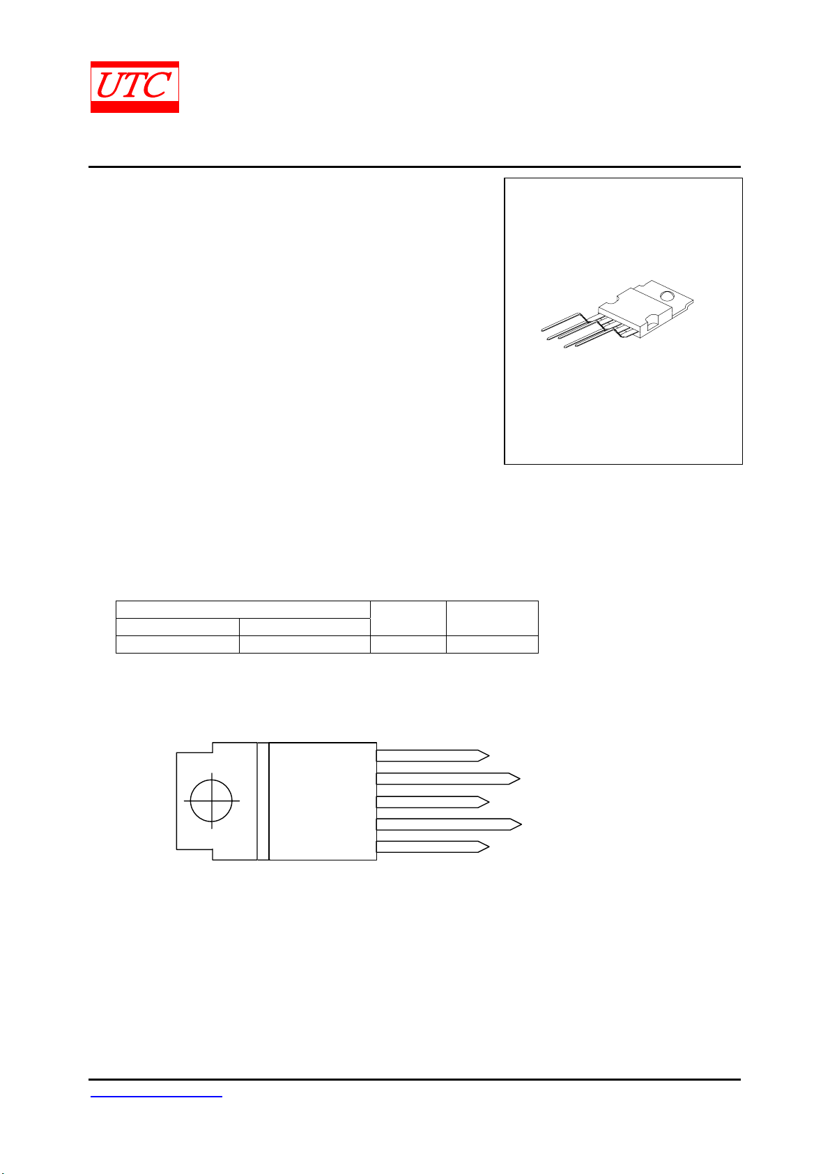
1
TO-220B
* High output power (50W Music Power IEC 268.3 Rules)
* High operating supply voltage (50V)
* Single or split supply operations
* Very low distortion
* Short circuit protection (OUT to GND)
* Thermal shutdown
ORDERING INFORMATION
Ordering Number
Normal Lead Free Plating
Package Packing
TDA2050-TB5-T TDA2050L-TB5-T TO-220B Tube
PIN CONFIGURATION
5
4
3
2
1
*Pb-free plating product number: TDA2050L
+V
S
OUTPUT
-V
S
INVERTING INPUT
NON INVERTING INPUT
*TAB CONNECTED TO PIN 3
www.unisonic.com.tw 1
Copyright © 2005 Unisonic Technologies Co., LTD QW-R107-036,A
Page 2
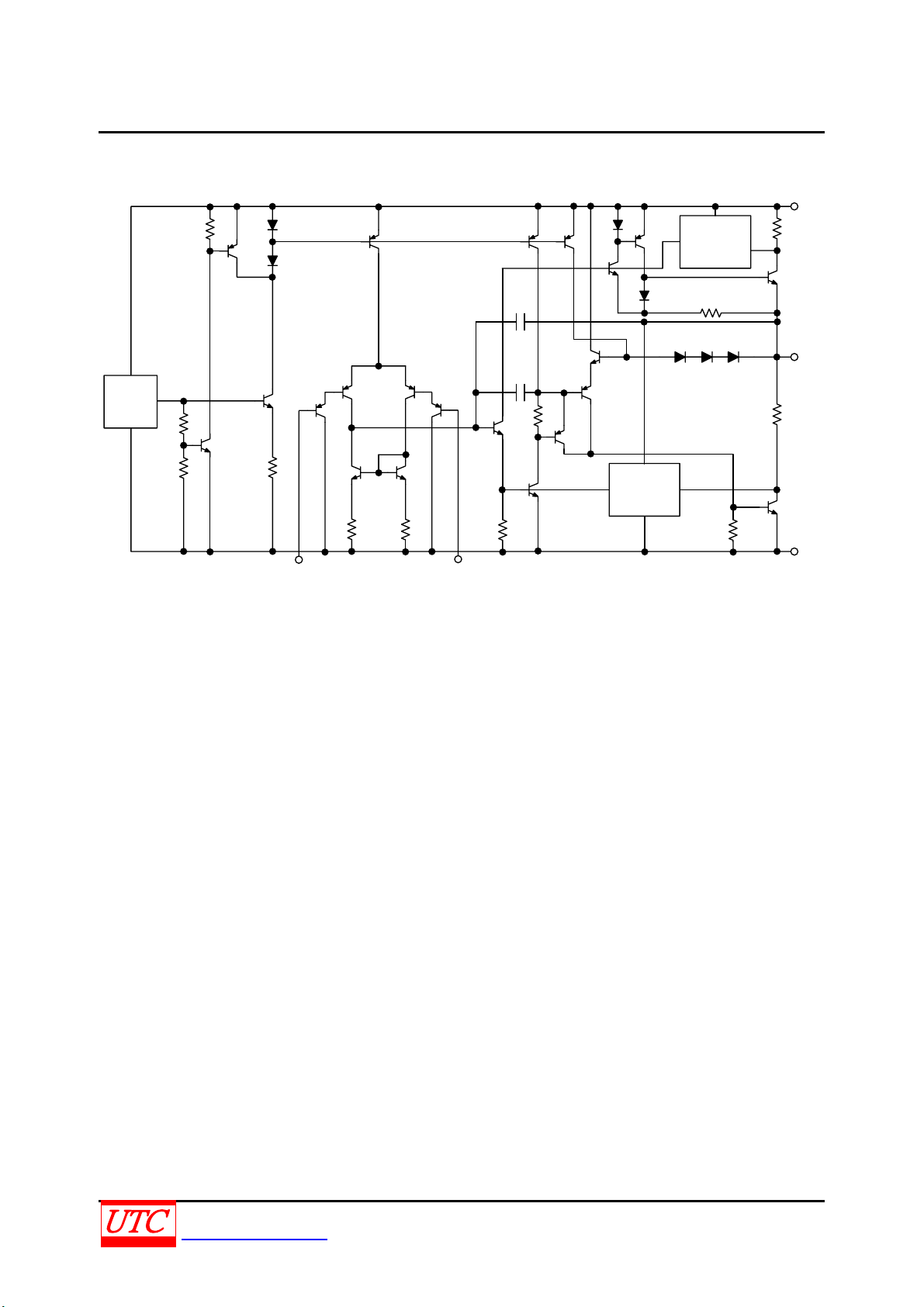
TDA2050 LINEAR INTEGRATED CIRCUIT
BLOCK DIAGRAM
5
SHORT
CIRC.
PROTECT.
4
V
REF
SHORT
CIRC.
PROTECT.
3
21
UNISONIC TECHNOLOGIES CO., LTD 2
www.unisonic.com.tw QW-R107-036,A
Page 3
TDA2050 LINEAR INTEGRATED CIRCUIT
ABSOLUTE MAXIMUM RATINGS
PARAMETER SYMBOL RATINGS UNIT
Supply Voltage VS ±25 V
Input Voltage VIN V
Differential Input Voltage V
Output Peak Current (internally limited) I
Power Dissipation TC= 75℃
±15
IN(DIFF)
5
OUT
P
25 W
D
Junction Temperature TJ +125
Storage Temperature T
-40 ~ +150
STG
Note:1.Absolute maximum ratings are those values beyond which the device could be permanently damaged.
Absolute maximum ratings are stress ratings only and functional device operation is not implied.
2.The device is guaranteed to meet performance specification within 0℃~70℃ operating temperature range
and assured by design from –40℃~85℃.
THERMAL DATA
PARAMETER SYMBOL RATINGS UNIT
θ
Thermal Resistance junction-case
ELECTRICAL CHARACTERISTICS
JC
S
℃
℃
℃
℃
3 ℃/W
(Refer to the Test Circuit, V
= ±18V, Ta = 25℃, f = 1 kHz, unless otherwise specified.)
S
PARAMETER SYMBOL TEST CONDITIONS MIN TYP MAX UNIT
Supply Voltage VS ±4.5 ±25 V
18
Quiescent Drain Current ID
V
= ±4.5V
S
V
= ±25V
S
21
50
90
mA
Input Bias Current IB VS = ±22V 0.4 0.5 µA
Input Offset Voltage V
Input Offset Current I
D = 0.5%
RMS Output Power
D = 10%
Music Power IEC268.3 RULES
VS = ±22V ±15 mV
IN(OS)
VS = ±22V ±200 nA
IN(OS)
27
= 4Ω
R
L
R
= 8Ω
L
R
= 8Ω, VS = ±22V
L
P
O
= 4Ω
R
L
R
= 8Ω
L
R
= 8Ω, VS = ±22V
L
D = 10%, T = 1s, V
= ±22.5V, RL = 4Ω 50
S
24
22
18
25
35
22
32
W
RL = 4Ω
Total Harmonic Distortion THD
f = 1kHz, P
f = 100Hz ~ 10kHz, P
R
= 8Ω, VS = ±22V
L
f = 1kHz, P
f = 100Hz ~ 10kHz, P
= 0.1 ~ 24W
O
O
= 0.1 ~ 20W
O
O
= 0.1 ~ 18W
= 0.1 ~ 15W
0.03 0.5
0.5
0.02
0.5
%
Slew Rate SR 5 8 V/µs
Open Loop Voltage Gain GV 80 dB
Closed Loop Voltage Gain GV 30 30.5 31 dB
Power Bandwidth (-3dB) BW RL = 4Ω, VIN= 200mV 20 ~ 80000 Hz
Total Input Noise eN
Curve A
B = 22Hz ~ 22kHz
4
5 10
µV
Input Resistance (pin 1) RIN 500 kΩ
Supply Voltage Rejection SVR RS = 22KΩ, f =100Hz, V
Efficiency η
PO = 28W, RL = 4Ω 65
P
= 25W, RL = 8Ω, VS = ±22V 67
O
=0.5Vrms 45 dB
RIPPLE
%
UNISONIC TECHNOLOGIES CO., LTD 3
www.unisonic.com.tw QW-R107-036,A
Page 4

TDA2050 LINEAR INTEGRATED CIRCUIT
TYPICAL APPLICATION CIRCUIT
FOR SPLIT SUPPLY APPLICATION SUGGESTIONS
+V
S
C1
22μF
V
IN
R1
22kΩ
R2
680Ω
C2
22μF
Figure.1 Split Supply Typical Application Circuit
The following table demonstrates the recommended values of the external components are those shown
on above circuit. Different values can be used.
COMPONENT PURPOSE
R1 Input Impedance 22kΩ
R2 Feedback Resistor 680Ω Decrease of Gain* Increase of Gain
R3 22kΩ Increase of Gain Decrease of Gain*
R4 Frequency Stability 2.2Ω Danger of Oscillations
C1 Input Decoupling DC 1µF Higher Low-frequency cut-off
C2
C3, C4 Supply Voltage Bypass 100nF Danger of Oscillations
C5, C6 Supply Voltage Bypass 220µF Danger of Oscillations
C7 Frequency Stability 0.47µF Danger of Oscillations
* The gain must be higher than 24dB
Inverting Input DC
Decoupling
C5
220μF
1
2
5
+
UTC
4
TDA2050
-
3
TYPICAL LARGER SMALLER
22µF
R3
22kΩ
C4
100nF
RECOMMENDED VALUE
Increase of Input Impedance Decrease of Input
Increase of Switch ON/OFF
Noise
C3
100nF
R4
2.2Ω
C7
0.47μF
C6
220μF
R
L
-V
S
Impedance
Higher Low-frequency cut-off
UNISONIC TECHNOLOGIES CO., LTD 4
www.unisonic.com.tw QW-R107-036,A
Page 5

TDA2050 LINEAR INTEGRATED CIRCUIT
TYPICAL APPLICATION CIRCUIT(CONT.)
FOR SINGLE SUPPLY APPLICATION SUGGESTIONS
+V
S
C2
1000μF
22kΩ
IN
R1
C1
2.2μF
R2
22kΩ
1000μF
R3
22kΩ
C4
22μF
C3
1
2
R4
680Ω
5
+
UTC
TDA2050
3
R5
22kΩ
C5
100nF
4
R6
2.2Ω
C6
0.47μF
C7
1000μF
R
Figure.2 Single Supply Typical Application Circuit
The following table demonstrates the recommended values of the external components are those shown
on above circuit. Different values can be used.
COMPONENT PURPOSE
R1, R2, R3 Biasing Resistor 22kΩ
R4 Feedback Resistor 22kΩ Increase of Gain Decrease of Gain*
R5 680Ω Decrease of Gain* Increase of Gain
R6 Frequency Stability 2.2Ω Danger of Oscillations
C1 Input Decoupling DC 2.2µF Higher Low-frequency cut-off
C2
C3 Supply Voltage Bypass 1000µF
C4
C5 Supply Voltage Bypass 100nF Danger of Oscillations
C6 Frequency Stability 0.47µF Danger of Oscillations
C7 Output DC Decoupling 1000µF Higher Low-frequency cut-off
* The gain must be higher than 24dB
NOTE: If the supply voltage is lower than 40V and the load is 8Ω(or more), a lower value of C2(i.e. 22µF) can be
used. C7 can be larger than 1000µF only if the supply voltage does not exceed 40V.
Supply Voltage
Rejection
Inverting Input DC
Decoupling
TYPICAL LARGER SMALLER
100µF
22µF
Worse Turn-off Transient
Worse Turn-on Delay
Increase of Switch ON/OFF
RECOMMENDED VALUE
Danger of Oscillations
Worse of Turn-off Transient
Higher Low-frequency cut-off
L
UNISONIC TECHNOLOGIES CO., LTD 5
www.unisonic.com.tw QW-R107-036,A
Page 6

TDA2050 LINEAR INTEGRATED CIRCUIT
TYPICAL CHARACTERISTICS (Split Supply Test Circuit, unless otherwise specified)
Output Power vs. Supply Voltage
40
RL= 8Ω
f = 1kHz
35
Output Power vs. Supply Voltage
40
RL= 4Ω
f = 1kHz
35
30
THD = 10%
25
(W)
20
O
P
+
15
10
5
0
10 20
15
V
(V)
S
Quiescent Current vs. Supply Voltage
60
RL= 4Ω
55
50
45
40
(mA)
D
I
35
30
25
20
10 20
15
V
(V)
S
THD = 0.5%
2550
2550
30
30
25
(W)
20
O
P
THD= 10%
15
10
5
0
10 20
15
V
(V)
S
Total Power Dissipation and Efficiency
vs. Output Power
40
VS= 18V
35
R
= 4Ω
L
f = 1kHz
30
25
20
(W)
D
P
15
10
5
0
10 20
15
P
O
2550
(W)
THD= 0.5%
2550
m
P
D
30 35
30
4030
80
70
60
50
40
30
20
10
0
m (%)
Total Power Dissipation and Efficiency
vs. Output Power
VS= 22V
28
R
= 8Ω
L
f = 1kHz
24
20
16
(W)
D
P
12
m
P
D
8
4
0
10 20
15
P
O
(W)
2550
30 35
80
70
60
50
40
30
20
10
0
m (%)
UNISONIC TECHNOLOGIES CO., LTD 6
www.unisonic.com.tw QW-R107-036,A
Page 7

TDA2050 LINEAR INTEGRATED CIRCUIT
UTC assumes no responsibility for equipment failures that result from using products at values that
exceed, even momentarily, rated values (such as maximum ratings, operating condition ranges, or
other parameters) listed in products specifications of any and all UTC products described or contained
herein. UTC products are not designed for use in life support appliances, devices or systems where
malfunction of these products can be reasonably expected to result in personal injury. Reproduction in
whole or in part is prohibited without the prior written consent of the copyright owner. The information
presented in this document does not form part of any quotation or contract, is believed to be accurate
and reliable and may be changed without notice.
UNISONIC TECHNOLOGIES CO., LTD 7
www.unisonic.com.tw QW-R107-036,A
 Loading...