

Page 1
32W Hi-Fi AUDIO POWERAMPLIFIER
HIGHOUTPUTPOWER
(50W MUSICPOWERIEC 268.3 RULES)
HIGHOPERATINGSUPPLYVOLTAGE(50V)
SINGLEOR SPLIT SUPPLYOPERATIONS
VERYLOWDISTORTION
SHORT CIRCUIT PROTECTION (OUT TO
GND)
THERMAL SHUTDOWN
TDA2050
Pentawatt
DESCRIPTION
The TDA 2050 is a monolithicintegrated circuit in
Pentawatt package, intended for use as an audio
classAB audio amplifier.Thanksto its high power
capability the TDA2050 is able to provide up to
35W true rms power into 4 ohm load @ THD =
10%, V
8ohmload @THD = 10%, V
= ±18V, f = 1KHz and up to 32W into
S
= ±22V, f = 1KHz.
S
Moreover, the TDA 2050 delivers typically 50W
music power into 4 ohm load over 1 sec at V
S
22.5V,f =1KHz.
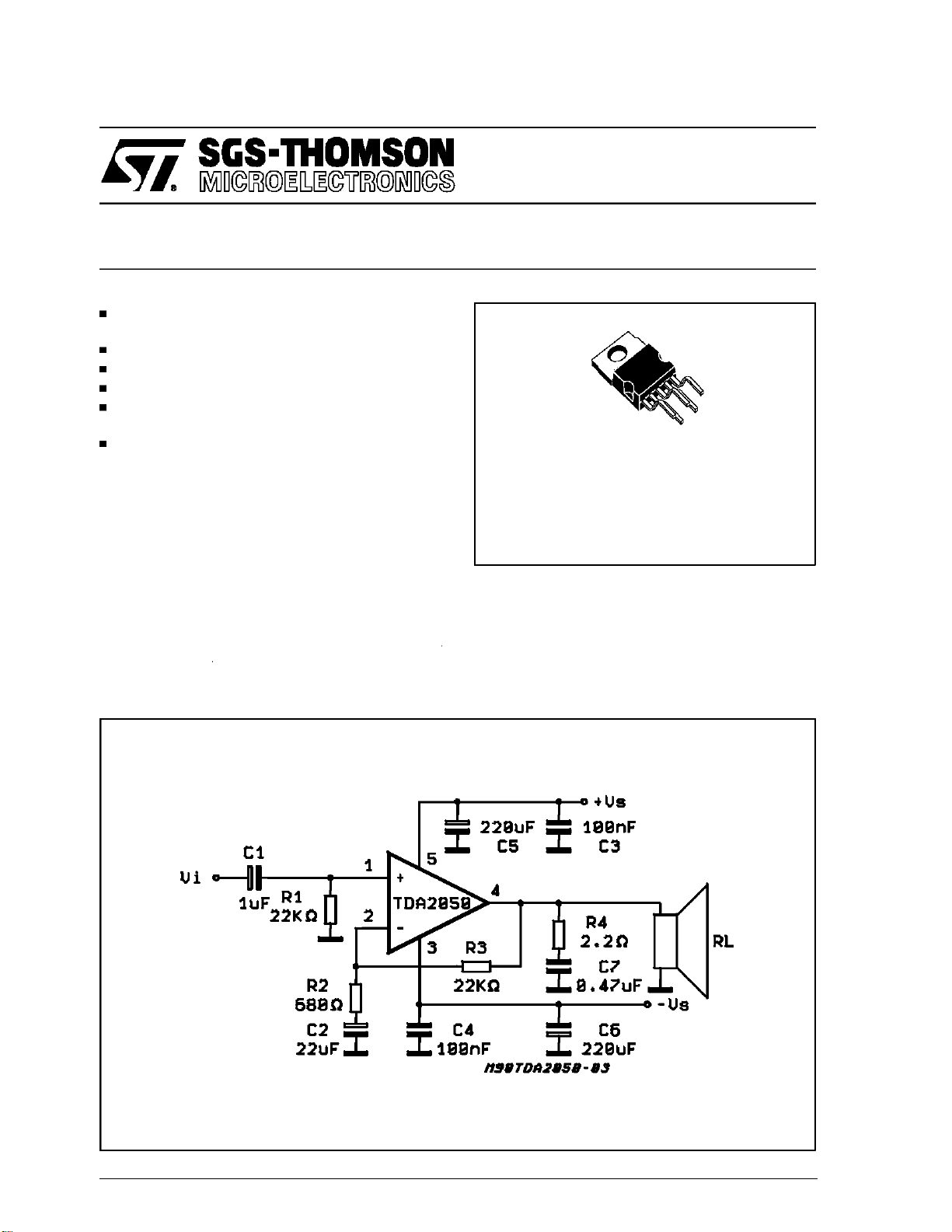
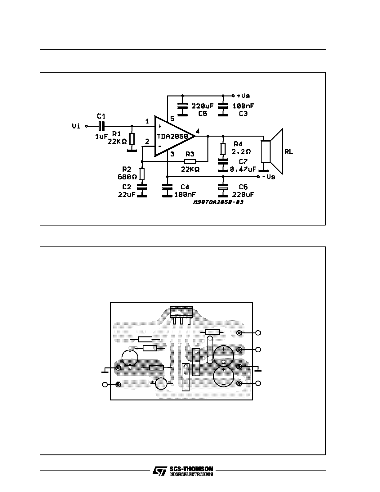
TEST AND APPLICATION CIRCUIT
ORDERING NUMBERS: TDA2050V
TDA2050H
Thehigh power and very low harmonic and crossover distortion (THD = 0.05% typ, @ V
P
= 0.1 to 15W, RL=8ohm, f = 100Hz to 15KHz)
O
make the device most suitable for both HiFi and
=
high class TV sets.
= ±22V,
S
March 1995
This is advanced information on anew product now in development or undergoing evaluation. Details are subject to change withoutnotice.
1/13
Page 2
TDA2050
ABSOLUTE MAXIMUMRATINGS
Symbol Parameter Value Unit
V
V
V
I
P
T
stg,Tj
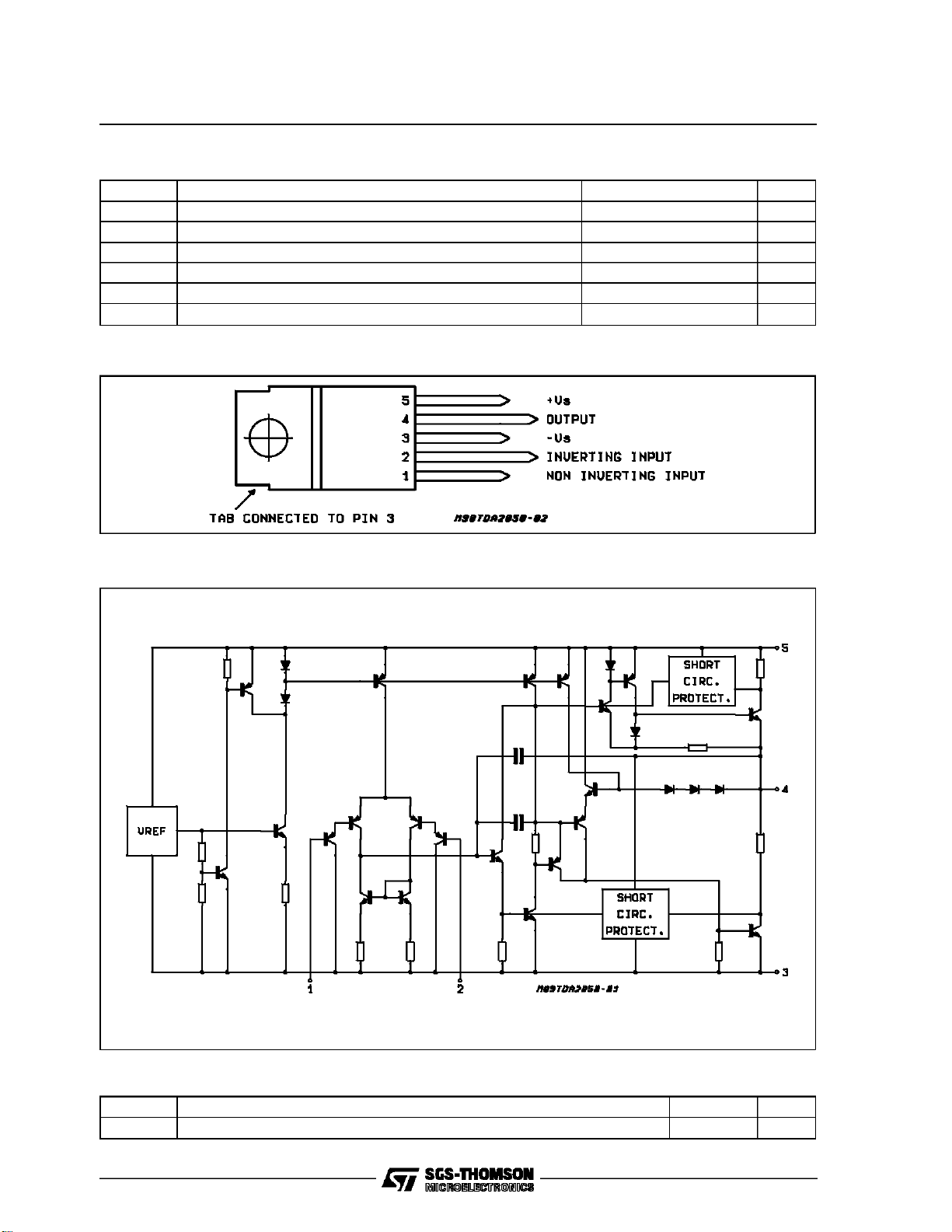
PIN CONNECTION (Top view)
Supply Voltage ±25 V
S
Input Voltage V
i
Differential Input Voltage ±15 V
i
Output Peak Current (internally limited) 5 A
O
Power DissipationT
tot
=75°C25W
CASE
S
Storage and JunctionTemperature -40 to 150 °C
SCHEMATICDIAGRAM
THERMAL DATA
Symbol Description Value Unit
Thermal Resistance junction-case Max 3 °C/W
2/13
R
th j-case
Page 3

TDA2050
ELECTRICAL CHARACTERISTICS (Refer to the Test Circuit, VS= ±18V, T
=25°C, f = 1 kHz; un-
amb
less otherwisespecified)
Symbol Parameter Test Condition Min. Typ. Max. Unit
V
V
I
OS
P
SR Slew Rate 5 8 V/µs
G
G
BW Power Bandwidth (-3dB) R
e
R
SVR Supply Voltage Rejection R
T
Supply Voltage Range ±4.5 ±25 V
S
Quiescent Drain Current VS= ±4.5V
I
d
Input Bias Current VS= ±22V 0.1 0.5 µA
I
b
Input Offset Voltage VS= ±22V ±15 mV
OS
V
S
= ±25V
30
55
Input Offset Current VS= ±22V ±200 nA
RMS OutputPower d =0.5%
O
R
=4Ω
L
R
=8Ω
L
V
=±22V RL=8Ω
S
24
22
28
18
25
d =10%
R
=4Ω
L
R
=8Ω
L
V
=±22V RL=8Ω
S
Music Power
IEC268.3 RULES
d Total Harmonic Distortion R
Open Loop VoltageGain 80 dB
V
Closed Loop Voltage Gain 30 30.5 31 dB
V
Total Input Noise curve A
N
d =10%; T = 1s
V
= ±22.5V; RL=4Ω 50 W
S
=4Ω
L
f = 1kHz, P
f = 100 Hz to 10kHz, P
= ±22V RL=8Ω
V
S
f = 1kHz, P
f = 100 Hz to 10kHz, P
=4Ω Vi= 200mV 20 to 80,000 Hz
L
= 0.1to 24W
O
= 0.1to 20W
O
= 0.1 to18W
O
= 0.1 to15W
O
B = 22Hz to 22kHz
Input Resistance (pin 1) 500 kΩ
i
= 22kΩ; f = 100Hz;
s
V
= 0.5Vrms 45 dB
ripple
η Efficiency P
Thermal Shut-down
sd-j
= 28W; RL=4Ω 65 %
O
= 25W; RL=8Ω;
P
O
V
=±22V 67 %
S
35
22
32
0.03 0.5
0.02
4
510
150 °C
Junction Temperature
50
90
0.5
0.5
mA
mA
W
W
W
W
W
W
%
%
%
%
µV
µV
3/13
Page 4
TDA2050
Figure1: Split Supply Typical Application Circuit
Figure2: P.C. Boardand ComponentsLayout of theCircuit of Fig. 1 (1:1)
TDA2050
R4
R3
R2
C2
R1
C4
C1
Vi
C7
C5
C3
C6
R
+Vs
-Vs
L
4/13
Page 5

TDA2050
SPLITSUPPLY APPLICATION SUGGESTIONS
The recommended values of the external compo-
of fig. 2. Differentvaluescan be used. The following table can helpthe designer.
nents are those shown on the application circuit
Component
R1 22kΩ Input Impedance Increase of Input
R2 680Ω Feedback Resistor Decrease ofGain (*) Increase of Gain
R3 22kΩ Increase of Gain Decrease of Gain (*)
R4 2.2Ω Frequency Stability Danger of Oscillations
C1 1µF Input Decoupling DC HigherLow-frequency
C2 22µF Inverting Input
C3
C4
C5
C6
C7 0.47µF Frequency Stability Danger of Oscillations
(*) The gain must behigher than 24dB
Recommended
Value
DC Decoupling
100nF Supply Voltage Bypass Danger of Oscillations
220µF Supply Voltage Bypass Danger of Oscillations
Purpose
PRINTEDCIRCUIT BOARD
The layout shown in fig. 2 should be adopted by
the designers. If different layouts are used, the
Larger than
Recommended Value
Impedance
Increase of Switch
ON/OFF Noise
Smaller than
Recommended Value
Decrease of Input
Impedance
cut-off
HigherLow-frequency
cut-off
ground points of input 1 and input 2 must be well
decoupledfrom the ground return of the output in
whicha highcurrentflows.
5/13
Page 6

TDA2050
Figure3: Single Supply Typical Application Circuit
Figure4: P.C. Boardand ComponentsLayout of theCircuit of Fig. 3 (1:1)
6/13
Page 7

SINGLESUPPLYAPPLICATIONSUGGESTIONS
The recommended values of the external components are those shown on the application circuit
TDA2050
of fig. 3. Differentvaluescan be used. The following table can helpthe designer.
Component
R1, R2, R3 22kΩ Biasing Resistor
R4 22kΩ
R5 680Ω Decrease of Gain (*) Increase of Gain
R6 2.2Ω Frequency Stability Danger of Oscillations
C1 2.2µF Input Decoupling DC HigherLow-frequency
C2 100µF Supply Voltage Rejection Worse Turn-off Transient
C3 1000µF Supply Voltage Bypass Danger of Oscillations
C4 22µF Inverting Input DC
C5 100nF Supply Voltage Bypass Danger of Oscillations
C6 0.47µF Frequency Stability Danger of Oscillations
C7 1000µF Output DC Decoupling HigherLow-frequency
(*) The gain must behigher than 24dB
Recommended
Value
Purpose
Feedback Resistors
Decoupling
NOTE
If the supply voltage is lower than 40V and the
load is 8ohm (or more) a lower value of C2 can
Larger than
Recommended Value
Increase of Gain Decrease of Gain (*)
Worse Turn-on Delay
Increase of Switching
ON/OFF
Smaller than
Recommended Value
cut-off
Worse of Turn-off
Transient
HigherLow-frequency
cut-off
cut-off
be used (i.e. 22µF).
C7 can be larger than 1000uF only if the supply
voltagedoesnot exceed 40V.
TYPICALCHARACTERISTICS (Split Supply Test Circuit unless otherwise specified)
Figure5: Output Power vs.SupplyVoltage
Figure6: Distortion vs. OutputPower
7/13
Page 8

TDA2050
Figure7: Output Power vs.SupplyVoltage
Figure.9: Distortion vs. Frequency
Figure8: Distortion vs. OutputPower
Figure10: Distortion vs. Frequency
Figure11: QuiescentCurrent vs. SupplyVoltage
8/13
Figure12: SupplyVoltageRejectionvs.Frequency
Page 9

TDA2050
Figure13: SupplyVoltage Rejection vs. Fre-
quency(Singlesupply) for Different
valuesof C2 (circuit of fig. 3)
Figure14: SupplyVoltage Rejection vs. Fre-
quency(Singlesupply) for Different
valuesof C2 (circuit of fig. 3)
Figure16: Total Power Dissipation and Effi-
ciencyvs. OutputPower
SHORTCIRCUIT PROTECTION
The TDA 2050 has an original circuit which limits
the current of the output transistors. The maximum output current is a function of the collector
emitter voltage; hence the output transistorswork
within their safe operating area. This function can
thereforebe consideredas being peak power limitingrather than simple current limiting.
It reduces the possibility that the device gets
damaged during an accidental short circuit from
AC output to ground.
Figure15: TotalPower Dissipation and Effi-
ciencyvs. OutputPower
THERMAL SHUTDOWN
The presence of a thermal limiting circuit offers
the following advantages:
1)An overload on the output (even if itis permanent), or an above limit ambient temperature
can be easily toleratedsince the Tj cannot be
higher than 150°C.
2)The heatsink can have a smaller factor of
safety compared with that of a conventional
circuit. There is no possibility of device damage due to high junction temperature. If for
any reason, the junction temperature increases up to 150°C, the thermal shutdown
simply reduces the power dissipation and the
current consumption.
The maximum allowable power dissipation depends upon the thermal resistance junction-ambi-
9/13
Page 10

TDA2050
ent. Fig. 17 shows this dissipable power as a
function of ambient temperature for differentthermal resistance.
Figure17: MaximumAllowablePower Dissipa-
tion vs. AmbientTemperature
MOUNTINGINSTRUCTIONS
The power dissipated in the circuit must be removedby adding anexternal heatsink.
Thanks to the PENTAWATT package, the
heatsink mounting operation is very simple, a
screw or a compression spring (clip) being suffi-
cient. Between the heatsink and the package is
better to insert a layer of silicon grease, to optimize the thermal contact;no electrical isolation is
needed between the two surfaces. Fig. 18 shows
an example of heatsink.
Dimensionsuggestion
The following table shows the length that the
heatsink in fig. 18 must have for several values
of Ptot and Rth.
P
(W) 12 8 6
tot
Lenght of heatsink (mm) 60 40 30
of heatsink (°C/W) 4.2 6.2 8.3
R
th
Figure18: Example of heat-sink
APPENDIX A
A.1 - MUSICPOWER CONCEPT
MUSIC POWER is (according to the IEC clauses
n.268-3of Jan 83) the maximumpower which the
amplifier is capable of producing across the rated
load resistance (regardless of non linearity)1 sec
afterthe applicationof a sinusoidal inputsignal of
frequency1 KHz.
According to this definition our method of measurementcomprises the followingsteps:
- Set the voltage supply at the maximum operating value;
- Applya input signal in the form of a 1KHz tone
burst of 1 sec duration: the repetition period
of the signalpulsesis 60 sec;
- Theoutput voltage is measured1 sec from the
startof thepulse;
- Increase the input voltage until the output signal shows a THD=10%;
- The music power is then V
Vout is the output voltage measured in the
condition of point 4 and RL is the rated load
impedance;
2
/RL, where
out
The target of this method is to avoid excessive
dissipationin the amplifier.
A.2 - INSTANTANEOUS POWER
Another power measurement (MAXIMUM IN-
STANTANEOUS OUTPUT POWER) was proposed by IEC in 1988 (IEC publication268-3 subclause19.A).
We give here only a brief extract of the concept,
and a circuituseful for the measurement.
The supply voltage is set at the maximum operating value.
The test signal consists of a sinusoidal signal
whose frequency is 20 Hz, to which are added alternate positive and negative pulses of 50 µs duration and 500 Hz repetition rate. The amplitude
ofthe 20 Hz signal is chosen todrivethe amplifier
to its voltageclipping limits,while theamplitudeof
the pulses takes the amplifier alternately into its
current-overloadlimits.
10/13
Page 11

TDA2050
A circuit for generating the test signal is given in
fig. 19.
The load networkconsists of a 40µF capacitor,in
series with a 1 ohm resistor. The capacitor limits
the current due to the 20 Hz signal to a low value,
whereas for he short pulses the effectiveload impedance is of the order of 1 ohm, and a high output currentis produced.
Using this signal and load network the measurement may be made without causing excessive
dissipation in the amplifier. The dissipation in the
1 ohm resistor is much lower than a rated output
Figure19: Testcircuitfor peak power measurement
power of the amplifier, because the duty-cycle of
the high output currentis low.
By feeding the amplifier output voltage to the Xplates of an oscilloscope, and the voltage across
the 1 ohm resistor (representing the output current) to the Y=plates, it is possible to read on the
display the value of the maximum instantaneous
output power.
Theresult of thistest applied at the TDA 2050 is:
PEAKPOWER= 100W typ
11/13
Page 12

TDA2050
PENTAWATT PACKAGEMECHANICAL DATA
DIM.
MIN. TYP. MAX. MIN. TYP. MAX.
mm inch
A 4.8 0.189
C 1.37 0.054
D 2.4 2.8 0.094 0.110
D1 1.2 1.35 0.047 0.053
E 0.35 0.55 0.014 0.022
F 0.8 1.05 0.031 0.041
F1 1 1.4 0.039 0.055
G 3.4 0.126 0.134 0.142
G1 6.8 0.260 0.268 0.276
H2 10.4 0.409
H3 10.05 10.4 0.396 0.409
L 17.85 0.703
L1 15.75 0.620
L2 21.4 0.843
L3 22.5 0.886
L5 2.6 3 0.102 0.118
L6 15.1 15.8 0.594 0.622
L7 6 6.6 0.236 0.260
M 4.5 0.177
M1 4 0.157
Dia 3.65 3.85 0.144 0.152
A
H3
L
L1
C
D1
Dia.
L7
L6
L2
L3L5
D
F1
H2
E
MM1
G1
G
F
12/13
Page 13

TDA2050
Information furnished is believed to be accurate and reliable. However, SGS-THOMSON Microelectronics assumes no responsibility for the
consequences of use of such informationnor for any infringement of patents or other rights of third parties which may result from its use. No
license is granted by implication or otherwise under any patent or patent rights of SGS-THOMSON Microelectronics. Specifications mentioned in thispublication are subject to change without notice. This publication supersedes and replaces all information previously supplied.
SGS-THOMSON Microelectronics products are not authorized for use as critical components in life support devices or systems without express writtenapproval of SGS-THOMSONMicroelectronics.
1994 SGS-THOMSON Microelectronics - All RightsReserved
PENTAWATTis a Registered Trademark of SGS-THOMSON Microelectronics
SGS-THOMSON Microelectronics GROUP OF COMPANIES
Australia - Brazil- France -Germany -Hong Kong - Italy - Japan - Korea -Malaysia -Malta - Morocco - The Netherlands- Singapore-
Spain - Sweden - Switzerland - Taiwan- Thaliand- United Kingdom - U.S.A.
13/13
 Loading...